Alignment and Adjustments
Samsung Electronics
5-7
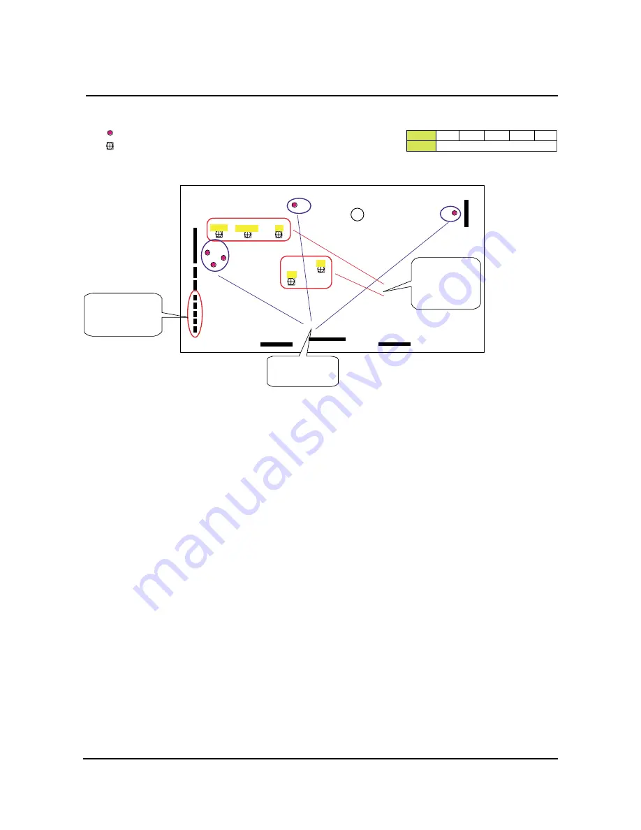
5-3 Voltage Adjustment
Output
Va
Vs c
Vs
Ve
Vs e t
Voltage
S ee the labels attached on the bas e c hass is
VR : Variable Res is tor
T e s t Point
S MPS
Vs
VSCAN
VSET
VA
VE
VSET
VSCAN
VE
VA
VS
Adjus t the S MPS
voltage us ing the
VR(Variable Re s istor)
Valida te the SMPS
voltage
Not us ed by this Mode l
Common us e with Other
Mode ls S MPS .
F an power s ource .
CN811
CN807
CN808
CN809
CN810
9
-. When the SMPS-PCB is replaced. the VA,VSCAN,VS,VE and VSET voltages
must be checked and adjusted to the proper to levels indicated on the panel sticker.
Notes
☞
Содержание D61B
Страница 10: ...3 2 Samsung Electronics MEMO ...
Страница 20: ...4 10 Samsung Electronics 4 11 1Sub field Process Address 1 4 12 1Sub field Process Address 2 Introduction PDP ...
Страница 21: ...Introduction PDP Samsung Electronics 4 11 4 13 1Sub field Process Address 3 4 14 1Sub field Process Address 4 ...
Страница 22: ...Introduction PDP 4 12 Samsung Electronics 4 15 1Sub field Process Address 5 4 16 1Sub field Process Address 6 ...
Страница 23: ...Introduction PDP Samsung Electronics 4 13 4 17 1Sub field Process Address 7 4 18 1Sub field Process Address 8 ...
Страница 24: ...Introduction PDP 4 14 Samsung Electronics 4 20 1Sub field Process Sustain 4 19 1Sub field Process Address 9 ...
Страница 30: ...4 20 Samsung Electronics MEMO ...
Страница 38: ...Alignment and Adjustments 2 8 Samsung Electronics MEMO ...
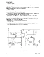
Страница 61: ...Fig 18 Chopper Circuit 6 22 Samsung Electronics Circuit Operation Description ...
Страница 85: ...8 8 Samsung Electronics MEMO ...
Страница 99: ...9 14 Samsung Electronics MEMO ...
Страница 105: ...Schematic Diagrams 10 6 Samsung Electronics 10 6 SMPS 1 This Document can not be used without Samsung s authorization ...
Страница 106: ...Samsung Electronics Schematic Diagrams 10 7 10 7 SMPS 2 ...
Страница 107: ...Schematic Diagrams 10 8 Samsung Electronics 10 8 SMPS 3 ...
Страница 108: ...Samsung Electronics Schematic Diagrams 10 9 10 9 SMPS 4 ...


