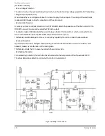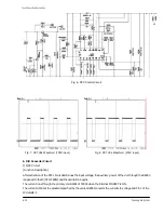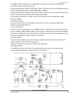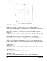
The current flows through the primary coil of T8531 and R8531 when the internal FET turns ON.
The current climbs at the gradient specified by the value L.
The R8531 converts the current to voltage and Pin 5 of the IC detects it.
The current increases and the FET turns OFF when the voltage at Pin 5 of the IC reaches the set point.
The IC behaves as a PRC (Pulse Ratio Control: fixed OFF width and controllable ON width) having 15
μ
sec for its
OFF width. The FET turns ON after the OFF width begins to oscillate.
Constant voltage regulation is performed by the photocoupler (PC8731) switching ON/OFF according to the
output voltage that is resistor divided (R8734, R8435, R8731 and R8736).
When the output voltage increases, the photocoupler (PC8731) turns ON to increase the voltage at Pin 5 of the IC
to narrow down the ON width for limited output voltage..
When the output voltage drops, it reverses to widen the ON width for increased output voltage.
[Protection Features]
·
-Over Voltage Protection
.The Latch circuit is activated to stop the circuit when the Vcc terminal voltage exceeds the OVP activating
voltage Vcc(OVP)=25.5V(TYP).
-Over Current Protection
The increased output current increases the current of the primary side.
Over Current protection is activated when this voltage exceeds the set point.
-Overheating Protection
The latch circuit is activated and stops the oscillation when the IC frame temperature exceeds 140
℃
.
Fig. 13. PRC Circuit
6-
18
Samsung Electronics
Circuit Operation Description
Содержание D61B
Страница 10: ...3 2 Samsung Electronics MEMO ...
Страница 20: ...4 10 Samsung Electronics 4 11 1Sub field Process Address 1 4 12 1Sub field Process Address 2 Introduction PDP ...
Страница 21: ...Introduction PDP Samsung Electronics 4 11 4 13 1Sub field Process Address 3 4 14 1Sub field Process Address 4 ...
Страница 22: ...Introduction PDP 4 12 Samsung Electronics 4 15 1Sub field Process Address 5 4 16 1Sub field Process Address 6 ...
Страница 23: ...Introduction PDP Samsung Electronics 4 13 4 17 1Sub field Process Address 7 4 18 1Sub field Process Address 8 ...
Страница 24: ...Introduction PDP 4 14 Samsung Electronics 4 20 1Sub field Process Sustain 4 19 1Sub field Process Address 9 ...
Страница 30: ...4 20 Samsung Electronics MEMO ...
Страница 38: ...Alignment and Adjustments 2 8 Samsung Electronics MEMO ...
Страница 61: ...Fig 18 Chopper Circuit 6 22 Samsung Electronics Circuit Operation Description ...
Страница 85: ...8 8 Samsung Electronics MEMO ...
Страница 99: ...9 14 Samsung Electronics MEMO ...
Страница 105: ...Schematic Diagrams 10 6 Samsung Electronics 10 6 SMPS 1 This Document can not be used without Samsung s authorization ...
Страница 106: ...Samsung Electronics Schematic Diagrams 10 7 10 7 SMPS 2 ...
Страница 107: ...Schematic Diagrams 10 8 Samsung Electronics 10 8 SMPS 3 ...
Страница 108: ...Samsung Electronics Schematic Diagrams 10 9 10 9 SMPS 4 ...


