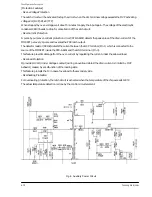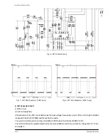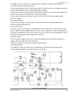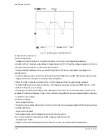
Fig. 3. Power Rectifier Circuit
3. Inrush Current Limit Circuit
When the input current is applied, the inrush current flows to charge the primary-side rectifying electrolytic
condenser. This current may damage the power supply by damaging the fuse or rectifier, or affect the internal
wirings. To prevent damage, the thermal fuse resistors (R8103, R8104, R8131), in the power line, limit the inrush
current. After the rectifying electrolytic condenser is charged, the relays RL8101 &, RL8102 are turned ON to
prevent the overheating of the fuses by the forwarding of the excess current.
If for some reason an error prevents RL8101, & RL 8102 from turning ON after the converter has been activated,
the circuit will be OPEN as R8103, & R8104 have thermal fuses and the power will be shut down safely without
smokinge or fire even when the inrush limit resistor heats-up.(If this occurs, replacement of R8103 and R8104 is
required.)
4.
Auxiliary Power Circuit
[Function Description]
By turning ON/OFF the MOS-FET inside the power control IC (STR0A6151), the charged current is transferred
from the electrolytic condenser (C8131) to the secondary part to generate the output voltage for STD-5V, the
power source for the control circuit and the PFC circuit.When the input voltage is applied, the IC will begin to
oscillate after the starting voltage is applied to Pin 2 of STR-A6151.
To control the output voltage, turn ON/OFF the photo-coupler PC8151 in order to regulate the output voltage at
1.26V when it is an alyzed by the IC8151 after being divided by R8153, RX8152 and R8154, R8155.
The coil between Pins 5 and 6 of the transformer T8131 generates the input power for the control IC of the PFC
circuit.
Samsung Electronics
6-
11
Circuit Operation Description
Содержание D61B
Страница 10: ...3 2 Samsung Electronics MEMO ...
Страница 20: ...4 10 Samsung Electronics 4 11 1Sub field Process Address 1 4 12 1Sub field Process Address 2 Introduction PDP ...
Страница 21: ...Introduction PDP Samsung Electronics 4 11 4 13 1Sub field Process Address 3 4 14 1Sub field Process Address 4 ...
Страница 22: ...Introduction PDP 4 12 Samsung Electronics 4 15 1Sub field Process Address 5 4 16 1Sub field Process Address 6 ...
Страница 23: ...Introduction PDP Samsung Electronics 4 13 4 17 1Sub field Process Address 7 4 18 1Sub field Process Address 8 ...
Страница 24: ...Introduction PDP 4 14 Samsung Electronics 4 20 1Sub field Process Sustain 4 19 1Sub field Process Address 9 ...
Страница 30: ...4 20 Samsung Electronics MEMO ...
Страница 38: ...Alignment and Adjustments 2 8 Samsung Electronics MEMO ...
Страница 61: ...Fig 18 Chopper Circuit 6 22 Samsung Electronics Circuit Operation Description ...
Страница 85: ...8 8 Samsung Electronics MEMO ...
Страница 99: ...9 14 Samsung Electronics MEMO ...
Страница 105: ...Schematic Diagrams 10 6 Samsung Electronics 10 6 SMPS 1 This Document can not be used without Samsung s authorization ...
Страница 106: ...Samsung Electronics Schematic Diagrams 10 7 10 7 SMPS 2 ...
Страница 107: ...Schematic Diagrams 10 8 Samsung Electronics 10 8 SMPS 3 ...
Страница 108: ...Samsung Electronics Schematic Diagrams 10 9 10 9 SMPS 4 ...


