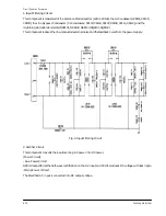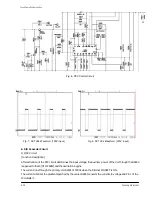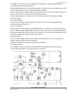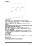
Fig. 10. Vds Waveform of the QRC Circuit
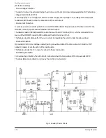
2) Resonance Circuit (Va, Vs)
[Function Description]
The behavior of both the Va, & Vs circuits are the same., The Va circuit is explained as an example.
Activation of the VL block provides voltage to the secondary coil (Pin 7-7), and the voltage is applied to Pin 1 (Vcc
terminal) of the resonance IC in order to start the oscillation.
The High Side FET (Q8332) and the Low Side FET (Q8333) turn ON in turn and transfer the energy to the
secondary side.
Constant voltage regulation occurs through the photocoupler (PC8901) turning ON/OFF according to the output
voltage that is resistor divided and is detected at the TR (Q8902).
PC8901 turns ON to draw the current from Pin 13 of the resonance IC as the output voltage increases.
The switching frequency increases, and the interval to charge the resonance condenser (C8338) shortens, which
results in limiting the output voltage.
Accordingly, when the output voltage drops, drawing the current from Pin 13 of the resonance IC which is not
available, the switching frequency drops, and the interval to charge the resonance condenser lengthens, resulting
in increased output voltage.
[Protection Features]
- Over Voltage Protection
The Latch circuit is activated to stop the circuit when the Vcc terminal voltage exceeds the OVP activating voltage
Vcc(OVP)=27V(Min).
- Over Current Protection
The increased output current increases the current of the primary side.
Over Current protection is activated when this voltage exceeds the set point.
- Overheating Protection
The latch circuit is activated and stops the oscillation when the IC frame temperature exceeds 150°C
6-
16
Samsung Electronics
Circuit Operation Description
Содержание D61B
Страница 10: ...3 2 Samsung Electronics MEMO ...
Страница 20: ...4 10 Samsung Electronics 4 11 1Sub field Process Address 1 4 12 1Sub field Process Address 2 Introduction PDP ...
Страница 21: ...Introduction PDP Samsung Electronics 4 11 4 13 1Sub field Process Address 3 4 14 1Sub field Process Address 4 ...
Страница 22: ...Introduction PDP 4 12 Samsung Electronics 4 15 1Sub field Process Address 5 4 16 1Sub field Process Address 6 ...
Страница 23: ...Introduction PDP Samsung Electronics 4 13 4 17 1Sub field Process Address 7 4 18 1Sub field Process Address 8 ...
Страница 24: ...Introduction PDP 4 14 Samsung Electronics 4 20 1Sub field Process Sustain 4 19 1Sub field Process Address 9 ...
Страница 30: ...4 20 Samsung Electronics MEMO ...
Страница 38: ...Alignment and Adjustments 2 8 Samsung Electronics MEMO ...
Страница 61: ...Fig 18 Chopper Circuit 6 22 Samsung Electronics Circuit Operation Description ...
Страница 85: ...8 8 Samsung Electronics MEMO ...
Страница 99: ...9 14 Samsung Electronics MEMO ...
Страница 105: ...Schematic Diagrams 10 6 Samsung Electronics 10 6 SMPS 1 This Document can not be used without Samsung s authorization ...
Страница 106: ...Samsung Electronics Schematic Diagrams 10 7 10 7 SMPS 2 ...
Страница 107: ...Schematic Diagrams 10 8 Samsung Electronics 10 8 SMPS 3 ...
Страница 108: ...Samsung Electronics Schematic Diagrams 10 9 10 9 SMPS 4 ...


