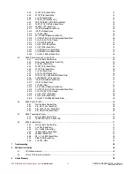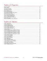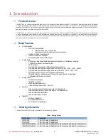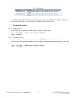
RTD Embedded Technologies, Inc.
| www.rtd.com
11
DM35418HR/DM35218HR
User’s Manual
BDM-610010041 Rev F
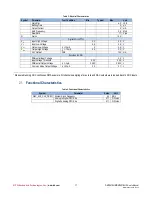
Table 3: Electrical Characteristics
Symbol
Parameter
Test Condition
Min
Typical
Max
Unit
Gain Error
±3 LSB
Settling Time
2 µs
Output Current
5 mA
-3dB Frequency
2.2 MHz
Slew Rate
17 V/µs
G
Gains
1,2,4
Digital I/O (LVTTL)
V
IL
Input High Voltage
2.0
3.3 V
V
IL
Input Low Voltage
-0.5
0.8 V
V
OL
Output Low Voltage
I
O
=-12mA
0
0.4 V
V
OH
Output High Voltage
I
O
= -12mA
2.4
3.3 V
3.3V Output
CN3
100 mA
SyncBus (LVDS)
Differential Input Voltage
2.4 V
Input Voltage Threshold
-0.05
0.05 V
Differential Output Voltage
I
O
= -4µA
0.480
0.650 V
Common Mode Output Voltage
I
O
=-20µA
0.3
2.1 V
1
Measured running ADC continuous DMA example. All channels sampling at max rate and DAC outputs were looped back to ADC inputs.
2.1
Functional Characteristics
Table 4: Functional Characteristics
Symbol
Parameter
Value
Unit
GBC_SYS_CLK_FREQ System Clock Frequency
40 MHz
Analog to Digital FIFO Size
511 D-Words
Digital to Analog FIFO Size
511 D-Words


