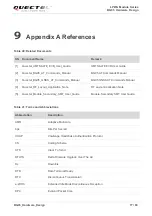
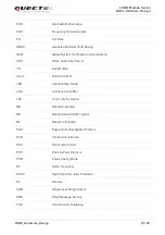
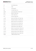
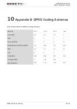
background image

LPWA Module Series 

                                                                                                  BG95  Hardware  Design


BG95_Hardware_Design                                                                                                                              70 / 80 
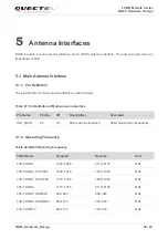
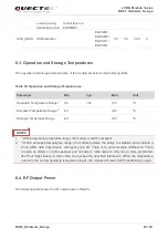
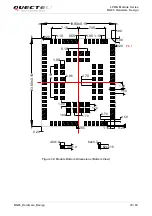


1.10

7.45

7.15

1.95

0.55

1.10

5.10

1.00

8.50

0.85

1.70

1.00

1.00

1.70

1.70

0.55

1.15

1.90

1.10

0.50

0.70

0.20

0.20

0.20

0.20

19.90±0.15

23.

60±0.15

40x1.0

40x1.0

62x0.7

62x1.15

1.00

1.00


Figure 32: Module Bottom Dimensions (Bottom View)   


Pin 1 

Содержание BG95 Series

Страница 1: ...BG95 Hardware Design LPWA Module Series Rev BG95_Hardware_Design_V1 0 Date 2019 05 15 Status Preliminary www quectel com...

Страница 2: ...ROVIDED IS BASED UPON CUSTOMERS REQUIREMENTS QUECTEL MAKES EVERY EFFORT TO ENSURE THE QUALITY OF THE INFORMATION IT MAKES AVAILABLE QUECTEL DOES NOT MAKE ANY WARRANTY AS TO THE INFORMATION CONTAINED H...

Страница 3: ...LPWA Module Series BG95 Hardware Design BG95_Hardware_Design 2 80 About the Document History Revision Date Author Description 1 0 2019 05 15 Lim PENG Garey XIE Initial...

Страница 4: ...Mode PSM 31 3 4 3 Extended Idle Mode DRX e I DRX 32 3 4 4 Sleep Mode 32 3 4 4 1 UART Application 32 3 5 Power Supply 33 3 5 1 Power Supply Pins 33 3 5 2 Decrease Voltage Drop 34 3 5 3 Monitor the Pow...

Страница 5: ...Connector for Antenna Installation 62 6 Electrical Reliability and Radio Characteristics 64 6 1 Absolute Maximum Ratings 64 6 2 Power Supply Ratings 64 6 3 Operation and Storage Temperatures 65 6 4 R...

Страница 6: ...NETLIGHT 48 TABLE 18 WORKING STATE OF NETLIGHT 48 TABLE 19 PIN DEFINITION OF STATUS 49 TABLE 20 DEFAULT BEHAVIORS OF RI 50 TABLE 21 PIN DEFINITION OF USB_BOOT INTERFACE 50 TABLE 22 PIN DEFINITION OF...

Страница 7: ...LPWA Module Series BG95 Hardware Design BG95_Hardware_Design 6 80 TABLE 42 DESCRIPTION OF DIFFERENT CODING SCHEMES 80 TABLE 43 GPRS MULTI SLOT CLASSES 81 TABLE 44 EDGE MODULATION AND CODING SCHEMES 83...

Страница 8: ...TRANSISTOR CIRCUIT 46 FIGURE 18 REFERENCE CIRCUIT OF PCM APPLICATION WITH AUDIO CODEC 47 FIGURE 19 REFERENCE CIRCUIT OF THE NETWORK STATUS INDICATOR 48 FIGURE 20 REFERENCE CIRCUIT OF STATUS 49 FIGURE...

Страница 9: ...pplications This document can help customers quickly understand the interface specifications electrical and mechanical details as well as other related information of BG95 To facilitate its applicatio...

Страница 10: ...t the airline staff for more restrictions on the use of wireless devices on boarding the aircraft Wireless devices may cause interference on sensitive medical equipment so please be aware of the restr...

Страница 11: ...ile device maintain at least a 20 cm separation between the EUT and the user s body and must not transmit simultaneously with any other antenna or transmitter 3 A label with the following statements m...

Страница 12: ...784748 D01 v07 section 8 Page 6 7 last two paragraphs A certified modular has the option to use a permanently affixed label or an electronic label For a permanently affixed label the module must be la...

Страница 13: ...equipment In cases where the manual is provided only in a form other than paper such as on a computer disk or over the Internet the information required by this section may be included in the manual i...

Страница 14: ...meet customers specific application demands Table 1 Version Selection for BG95 Series Module Table 2 Frequency Bands and GNSS Types of BG95 Series Module Version Cat M1 VoLTE Cat NB2 3 NB1 GSM Wi Fi P...

Страница 15: ...25 B26 B28 B66 B71 B85 EGPRS 850 900 1800 1900MHz Power Class 5 20dBm GPS GLONASS BeiDou Galileo BG95 N1 Cat NB2 Only LTE FDD B1 B2 B3 B4 B5 B8 B12 B13 B18 B19 B20 B25 B26 B28 B66 B71 B85 Power Class...

Страница 16: ...h as smart metering tracking system security wireless POS etc BG95 is an SMD type module which can be embedded into applications through its 102 LGA pads It supports internet service protocols like TC...

Страница 17: ...F bandwidth for LTE Cat M1 Support 200KHz RF bandwidth for LTE Cat NB2 Support SISO in DL direction Cat M1 Max 589Kbps DL 1 12Mbps UL Cat NB2 Max 136Kbps DL 150Kbps UL GSM Features GPRS Support GPRS m...

Страница 18: ...x 7 x 8 x 9 x UART Interfaces Main UART Used for data transmission and AT command communication 115200bps baud rate by default The default frame format is 8N1 8 data bits no parity 1 stop bit Support...

Страница 19: ...temperature levels the module will meet 3GPP specifications again 2 3 Functional Diagram The following figure shows a block diagram of BG95 and illustrates the major functional parts Power management...

Страница 20: ...ports using of only one ADC interface at a time either ADC0 or ADC1 Currently only ADC0 is enabled and ADC1 will be enabled in the next hardware design version 4 means under development 2 4 Evaluation...

Страница 21: ...t can be connected to customers cellular application platforms The following sub chapters will provide detailed description of interfaces listed below Power supply U SIM interface USB interface UART i...

Страница 22: ...GND USIM_CLK USIM_DATA USIM_RST USIM_VDD RI DCD CTS TXD RXD VBAT_BB VBAT_BB USIM_GND GND RESERVED 31 29 28 27 26 23 22 21 20 19 10 9 USB_DP USB_VBUS ADC1 1 GND RESERVED RESERVED RTS I2C_SCL I2C_SDA 8...

Страница 23: ...Qualcomm chipset PWRKEY should never be pulled down to GND permanently 3 3 RESET_N will be supported in the next hardware design version 4 Keep all RESERVED pins and unused pins unconnected 5 GND pins...

Страница 24: ...ule s RF part BG95 M1 M2 N1 Vmax 4 8V Vmin 2 4V Vnorm 3 3V BG95 M3 Vmax 4 3V Vmin 3 3V Vnorm 3 8V VDD_EXT 29 PO 1 8V output power supply for external circuit Vnorm 1 8V IOmax 50mA Power supply for ext...

Страница 25: ...status VOHmin 1 35V VOLmax 0 45V 1 8V power domain If unused keep this pin open USB Interface Pin Name Pin No I O Description DC Characteristics Comment USB_VBUS 8 PI USB detection Vmax 5 25V Vmin 3 0...

Страница 26: ...er domain If unused keep this pin open RXD 34 DI Receive data VILmin 0 3V VILmax 0 6V VIHmin 1 2V VIHmax 2 0V 1 8V power domain If unused keep this pin open TXD 35 DO Transmit data VOLmax 0 45V VOHmin...

Страница 27: ...6V VIHmin 1 2V VIHmax 2 0V 1 8V power domain If unused keep this pin open PCM Interface Pin Name Pin No I O Description DC Characteristics Comment PCM_CLK 4 DO PCM clock output VOLmax 0 45V VOHmin 1...

Страница 28: ...GPIO16 16 IO General purpose input output interface VOLmax 0 45V VOHmin 1 35V VILmin 0 3V VILmax 0 6V VIHmin 1 2V VIHmax 2 0V 1 8V power domain If unused keep this pin open GPIO25 25 IO General purpos...

Страница 29: ...Voltage range 0 3V to 1 8V ADC0 and ADC1 cannot be used simultaneously BG95 supports using of only one ADC interface at a time either ADC0 or ADC1 Currently only ADC0 is enabled and ADC1 will be enabl...

Страница 30: ...is rebooted When PSM_IND is in high voltage level the module is in normal operation state when it is in low voltage level the module is in PSM 5 Keep all RESERVED pins and unused pins unconnected 6 me...

Страница 31: ...eing available for mobile terminating data and or network originated procedures within a certain delay dependent on the DRX cycle value Airplane Mode AT CFUN 4 or W_DISABLE pin can set the module into...

Страница 32: ...s similar to power off but the module remains registered on the network and there is no need to re attach or re establish PDN connections So BG95 in PSM cannot immediately respond users requests When...

Страница 33: ...he subscription data from the HSS may also provide different values of the e I DRX parameters than what was requested by the UE If the EPC accepts the use of e I DRX the UE applies e I DRX based on th...

Страница 34: ...the sleep state of the host can be configured to high level or low level detection Please refer to AT QCFG apready command in document 2 for details means under development 3 5 Power Supply 3 5 1 Pow...

Страница 35: ...3V Ripple Drop Burst Transmission Figure 4 Power Supply Limits during Burst Transmission To decrease voltage drop a bypass capacitor of about 100 F with low ESR should be used and a multi layer cerami...

Страница 36: ...nt and suitable reverse stand off voltage and also it is recommended to place it as close to the VBAT pins as possible The following figure shows the star structure of the power supply Module VBAT_RF...

Страница 37: ...0ms 10nF Figure 6 Turn on the Module Using Driving Circuit Another way to control the PWRKEY is using a button directly When pressing the key electrostatic strike may generate from the finger Therefor...

Страница 38: ...t voltage is the internal voltage minus a diode drop in the chipset Therefore the expected output voltage of PWRKEY is 1 5V 3 PWRKEY should never be pulled down to GND permanently 3 6 2 Turn off Modul...

Страница 39: ...s similar to turning off the module via PWRKEY pin Please refer to document 2 for details about AT QPOWD command 3 7 Reset the Module RESET_N is used to reset the module and will be supported in the n...

Страница 40: ...iming of Reset Module The recommended circuit is similar to the PWRKEY control circuit An open drain collector driver or button can be used to control the RESET_N pin Reset pulse RESET_N 4 7K 47K 2s 3...

Страница 41: ...rts low level and high level detections and is disabled by default Please refer to document 2 about AT QSIMDET command for details The following figure shows a reference design of U SIM interface with...

Страница 42: ...a 6 pin U SIM card connector is illustrated in the following figure Figure 14 Reference Circuit of U SIM Interface with a 6 Pin U SIM Card Connector In order to enhance the reliability and availabili...

Страница 43: ...The 33pF capacitors are used for filtering interference of GSM 900MHz Please note that the U SIM peripheral circuit should be close to the U SIM card connector The pull up resistor on USIM_DATA line...

Страница 44: ...nd also these resistors should be placed close to each other The extra stubs of trace must be as short as possible The following principles should be complied with when design the USB interface so as...

Страница 45: ...S UART interface supports 115200bps baud rate by default and is used for GNSS data and NMEA sentences output The following tables show the pin definition of the three UART interfaces Table 12 Pin Defi...

Страница 46: ...rs application is equipped with a 3 3V UART interface A level translator TXS0108EPWR provided by Texas Instruments is recommended The following figure shows a reference design of the Main UART interfa...

Страница 47: ...it with Translator Chip Please visit http www ti com for more information Another example with transistor translation circuit is shown as below The circuit design of dotted line section can refer to t...

Страница 48: ...g figure shows a reference design of PCM and I2C interfaces with an external codec IC Figure 18 Reference Circuit of PCM Application with Audio Codec means under development Pin Name Pin No I O Descri...

Страница 49: ...le 17 Pin Definition of NETLIGHT Table 18 Working State of NETLIGHT A reference circuit is shown in the following figure Figure 19 Reference Circuit of the Network Status Indicator Pin Name Pin No I O...

Страница 50: ...Table 19 Pin Definition of STATUS The following figure shows a reference circuit of STATUS Figure 20 Reference Circuit of STATUS 3 14 Behaviors of RI AT QCFG risignaltype physical command can be used...

Страница 51: ...AT port 2 means under development 3 15 USB_BOOT Interface BG95 provides a USB_BOOT pin During development or factory production USB_BOOT can force the module to boot from USB port for firmware upgrade...

Страница 52: ...T QADC 0 command can be used to read the voltage value on the ADC being used For more details about the AT command please refer to document 2 In order to improve the accuracy of ADC voltage values the...

Страница 53: ...than 1 3 17 GPIO Interfaces The module provides six general purpose input and output GPIO interfaces AT QCFG gpio command can be used to configure corresponding GPIO pin s status For more details abou...

Страница 54: ...95_Hardware_Design 53 80 The following table describes the characteristics of GPIO interfaces Table 25 Logic Levels of GPIO Interfaces means under development Parameter Min Max Unit VIL 0 3 0 6 V VIH...

Страница 55: ...by default By default BG95 GNSS engine is switched off It has to be switched on via AT command For more details about GNSS engine technology and configurations please refer to document 3 4 2 GNSS Perf...

Страница 56: ...cold start command 4 3 Layout Guidelines The following layout guidelines should be taken into account in customers designs Maximize the distance between GNSS antenna and main antenna Digital circuits...

Страница 57: ...le 27 Pin Definition of Main Antenna Interface 5 1 2 Operating Frequency Table 28 BG95 Operating Frequency Pin Name Pin No I O Description Comment ANT_MAIN 60 IO Main antenna interface 50 characterist...

Страница 58: ...performance and the type matching components R1 C1 C2 should be placed as close to the antenna as possible The capacitors are not mounted by default LTE FDD B13 777 787 746 756 MHz LTE FDD B14 1 788 7...

Страница 59: ...RF traces is usually determined by the trace width W the materials dielectric constant the distance between signal layer and reference ground H and the clearance between RF trace and ground S Microstr...

Страница 60: ...dware_Design 59 80 Figure 24 Coplanar Waveguide Line Design on a 2 layer PCB Figure 25 Coplanar Waveguide Line Design on a 4 layer PCB Layer 3 as Reference Ground Figure 26 Coplanar Waveguide Line Des...

Страница 61: ...er joint The reference ground of RF traces should be complete Meanwhile adding some ground vias around RF traces and the reference ground could help to improve RF performance The distance between the...

Страница 62: ...ircuit is not needed 5 3 Antenna Installation 5 3 1 Antenna Requirements The following table shows the requirements on main antenna and GNSS antenna Table 31 Antenna Requirements Antenna Type Requirem...

Страница 63: ...NB2 only 4 means under development 5 3 2 Recommended RF Connector for Antenna Installation If RF connector is used for antenna connection it is recommended to use the U FL R SMT connector provided by...

Страница 64: ...BG95_Hardware_Design 63 80 Figure 29 Mechanicals of U FL LP Connectors The following figure describes the space factor of mated connector Figure 30 Space Factor of Mated Connector Unit mm For more de...

Страница 65: ...table Table 32 Absolute Maximum Ratings 6 2 Power Supply Ratings Table 33 Power Supply Ratings Parameter Min Max Unit VBAT_BB 0 5 6 0 V VBAT_RF 0 3 6 0 V USB_VBUS 0 3 5 5 V Voltage at Digital Pins 0 3...

Страница 66: ...ecoverable malfunction There are also no effects on radio spectrum and no harm to radio network Only one or more parameters like Pout might reduce in their value and exceed the specified tolerances Wh...

Страница 67: ...Max Min LTE FDD B1 B2 B3 B4 B5 B8 B12 B13 B14 1 B18 B19 B20 B25 B26 B27 1 B28 B66 B71 2 B85 20dBm 2dB 39dBm GSM850 EGSM900 33dBm 2dB 5dBm 5dB DCS1800 PCS1900 30dBm 2dB 0dBm 5dB GSM850 EGSM900 8 PSK 2...

Страница 68: ...essing handling and operation of any application that incorporates the module The following table shows the electrostatic discharge characteristics of BG95 module LTE FDD B13 TBD 99 3 TBD 107 5 LTE FD...

Страница 69: ...rdware Design BG95_Hardware_Design 68 80 Table 37 Electrostatic Discharge Characteristics 25 C 45 Relative Humidity Tested Points Contact Discharge Air Discharge Unit VBAT GND TBD TBD kV Main GNSS Ant...

Страница 70: ...ons This chapter describes the mechanical dimensions of the module All dimensions are measured in mm and the tolerances for dimensions without tolerance values are 0 05mm 7 1 Mechanical Dimensions of...

Страница 71: ..._Design 70 80 1 10 7 45 7 15 1 95 0 55 1 10 5 10 1 00 8 50 0 85 1 70 1 00 1 00 1 70 1 70 0 55 1 15 1 90 1 10 0 50 0 70 0 20 0 20 0 20 0 20 19 90 0 15 23 60 0 15 40x1 0 40x1 0 62x0 7 62x1 15 1 00 1 00...

Страница 72: ...0 85 9 60 9 70 11 03 11 03 4 25 4 25 5 95 5 95 7 65 7 65 2 55 2 55 9 18 9 18 4 25 5 95 4 25 5 95 0 85 0 20 0 20 0 20 0 20 19 90 0 15 1 00 1 00 23 60 0 15 Figure 33 Recommended Footprint Top View 1 Fo...

Страница 73: ...are_Design 72 80 7 3 Design Effect Drawings of the Module Figure 34 Top View of the Module Figure 35 Bottom View of the Module These are renderings of BG95 module For authentic appearance please refer...

Страница 74: ...e factory environment of 30 C 60 RH Stored at 10 RH 3 Devices require baking before mounting if any circumstance below occurs When the ambient temperature is 23 C 5 C and the humidity indication card...

Страница 75: ...the peak reflow temperature is 238 245 C and the absolute maximum reflow temperature is 245 C To avoid damage to the module caused by repeated heating it is strongly recommended that the module should...

Страница 76: ...the devices are ready to be soldered onto the application The reel is 330mm in diameter and each reel contains 250 modules The following figures show the packaging details measured in mm Figure 37 Ta...

Страница 77: ...ign 76 80 PS 6 DETAIL A DETAIL A Figure 38 Reel Dimensions Table 39 Reel Packaging Model Name MOQ for MP Minimum Package 250pcs Minimum Package x 4 1000pcs BG95 250pcs Size 370mm 350mm 56mm N W 0 61kg...

Страница 78: ...mands_Manual BG95 GNSS AT Commands Manual 4 Quectel_RF_Layout_Application_Note RF Layout Application Note 5 Quectel_Module_Secondary_SMT_User_Guide Module Secondary SMT User Guide Abbreviation Descrip...

Страница 79: ...put Inorm Normal Current LED Light Emitting Diode LNA Low Noise Amplifier LTE Long Term Evolution MO Mobile Originated MS Mobile Station GSM engine MT Mobile Terminated PAP Password Authentication Pro...

Страница 80: ...Maximum Input High Level Voltage Value VIHmin Minimum Input High Level Voltage Value VILmax Maximum Input Low Level Voltage Value VILmin Minimum Input Low Level Voltage Value VImax Absolute Maximum In...

Страница 81: ...mes Table 42 Description of Different Coding Schemes Scheme CS 1 CS 2 CS 3 CS 4 Code Rate 1 2 2 3 3 4 1 USF 3 3 3 3 Pre coded USF 3 6 6 12 Radio Block excl USF and BCS 181 268 312 428 BCS 40 16 16 16...

Страница 82: ...e first number indicates the amount of downlink timeslots while the second number indicates the amount of uplink timeslots The active slots determine the total number of slots the GPRS device can use...

Страница 83: ...rdware Design BG95_Hardware_Design 82 80 15 5 5 NA 16 6 6 NA 17 7 7 NA 18 8 8 NA 19 6 2 NA 20 6 3 NA 21 6 4 NA 22 6 4 NA 23 6 6 NA 24 8 2 NA 25 8 3 NA 26 8 4 NA 27 8 4 NA 28 8 6 NA 29 8 8 NA 30 5 1 6...

Страница 84: ...SK 13 4kbps 26 8kbps 53 6kbps CS 3 GMSK 15 6kbps 31 2kbps 62 4kbps CS 4 GMSK 21 4kbps 42 8kbps 85 6kbps MCS 1 GMSK C 8 80kbps 17 60kbps 35 20kbps MCS 2 GMSK B 11 2kbps 22 4kbps 44 8kbps MCS 3 GMSK A 1...

Отзывы: