


LPWA Module Series
BG95 Hardware Design
BG95_Hardware_Design 58 / 80
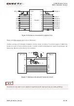
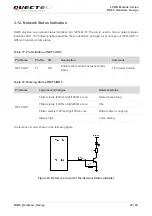
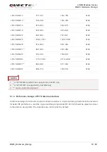
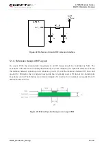
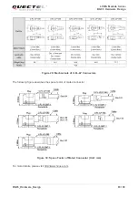
Figure 22: Reference Circuit of RF Antenna Interface
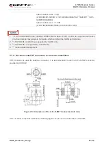
5.1.4. Reference Design of RF Layout
For user’s PCB, the characteristic impedance of all RF traces should be controlled as 50
Ω
. The
impedance of the RF traces is usually determined by the trace width (W), the materials’ dielectric constant,
the distance between signal layer and reference ground (H), and the clearance between RF trace and
ground (S). Microstrip line or coplanar waveguide line is typically used in RF layout for characteristic
impedance control. The following are reference designs of microstrip line or coplanar waveguide line with
different PCB structures.
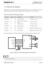
Figure 23: Microstrip Line Design on a 2-layer PCB


