


LPWA Module Series
BG95 Hardware Design
BG95_Hardware_Design 24 / 80
never be pulled down
to GND permanently.
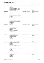
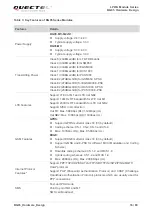
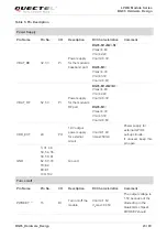
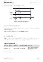
Reset
Pin Name
Pin No.
I/O
Description
DC Characteristics
Comment
RESET_N
2)
17
DI
Reset the
module
V
IL
max=0.45V
RESET_N will be
supported in the next
hardware design
version.
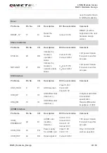
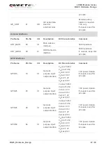
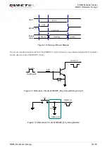
Status Indication
Pin Name
Pin No.
I/O
Description
DC Characteristics
Comment
STATUS 20 DO
Indicate the
module’s
operation
status
V
OH
min=1.35V
V
OL
max=0.45V
1.8V power domain.
If unused, keep this
pin open.
NETLIGHT 21
DO
Indicate the
module’s
network activity
status
V
OH
min=1.35V
V
OL
max=0.45V
1.8V power domain.
If unused, keep this
pin open.
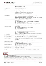
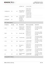
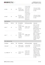
USB Interface
Pin Name
Pin No.
I/O
Description
DC Characteristics
Comment
USB_VBUS 8
PI USB
detection
Vmax=5.25V
Vmin=3.0V
Vnorm=5.0V
USB_DP 9
IO
USB differential
data bus (+)
Compliant with USB
2.0 standard
specification.
Require differential
impedance of 90
Ω
.
USB_DM 10
IO
USB differential
data bus (-)
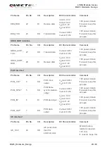
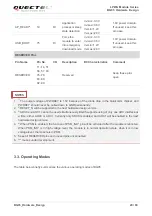
(U)SIM Interface
Pin Name
Pin No.
I/O
Description
DC Characteristics
Comment
USIM_
PRESENCE*
42 DI
(U)SIM card
insertion
detection
V
IL
min=-0.3V
V
IL
max=0.6V
V
IH
min=1.2V
V
IH
max=2.0V
1.8V power domain.
If unused, keep this
pin open.
USIM_VDD 43
PO
Power supply
for (U)SIM card
Vmax=1.9V
Vmin=1.7V
Only 1.8V (U)SIM
card is supported.
USIM_RST
44
DO
Reset signal of
V
OL
max=0.45V


