


LPWA Module Series
BG95 Hardware Design
BG95_Hardware_Design 34 / 80
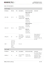
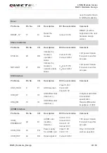
Table 7: VBAT and GND Pins
3.5.2. Decrease Voltage Drop
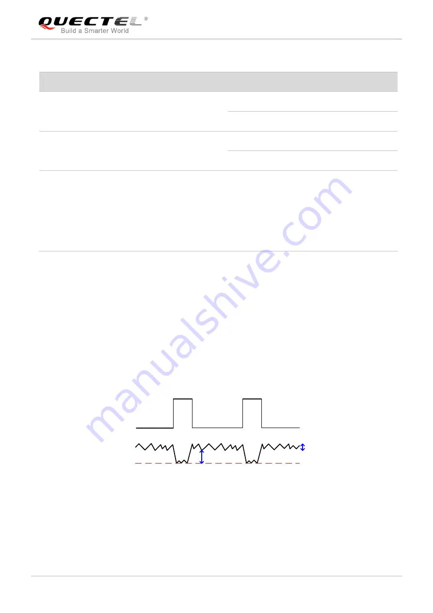
BG95-M1/-M2/-N1:
The power supply range of BG95-M1/-M2/-N1 is from 2.4V to 4.8V. Please make
sure that the input voltage will never drop below 2.4V.
BG95-M3:
The power supply range of the BG95-M3 is from 3.3V to 4.3V. Please make sure that the
input voltage will never drop below 3.3V.
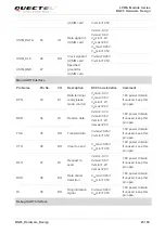
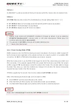
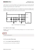
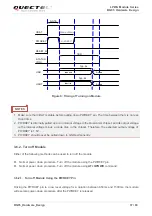
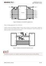
The following figure shows the voltage drop during burst transmission in 2G network of BG95-M3 module.
The voltage drop will be less in LTE Cat M1 and/or LTE Cat NB2 networks.
VBAT
Burst
Transmission
Min.3.3V
Ripple
Drop
Burst
Transmission
Figure 4: Power Supply Limits during Burst Transmission
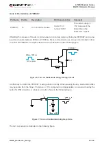
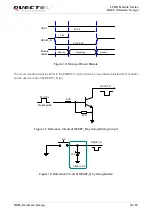
To decrease voltage drop, a bypass capacitor of about 100µF with low ESR should be used, and a
multi-layer ceramic chip capacitor (MLCC) array should also be reserved due to its low ESR. It is
recommended to use three ceramic capacitors (100nF, 33pF, 10pF) for composing the MLCC array, and
place these capacitors close to VBAT pins. The main power supply from an external application has to be
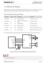
Pin Name
Pin No.
Description
Module
Min. Typ. Max.
Unit
VBAT_RF 52,
53
Power supply for the
module’s RF part
BG95-M1/-M2/-N1 2.4 3.3 4.8 V
BG95-M3 3.3
3.8
4.3
V
VBAT_BB 32,
33
Power supply for the
module’s baseband
part
BG95-M1/-M2/-N1 2.4 3.3 4.8 V
BG95-M3 3.3
3.8
4.3
V
GND
3, 31, 48, 50,
54, 55, 58,
59, 61, 62,
67~74,
79~82,
89~91,
100~102
Ground
-
-
-
-


