


LPWA Module Series
BG95 Hardware Design
BG95_Hardware_Design 23 / 80
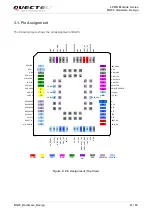
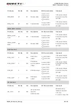
Table 5: Pin Description
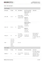
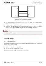
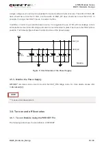
Power Supply
Pin Name
Pin No.
I/O
Description
DC Characteristics
Comment
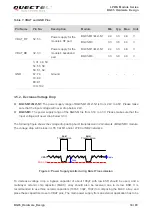
VBAT_BB 32,
33 PI
Power supply
for the module’s
baseband part
BG95-M1/-M2/-N1:
Vmax=4.8V
Vmin=2.4V
Vnorm=3.3V
BG95-M3:
Vmax=4.3V
Vmin=3.3V
Vnorm=3.8V
VBAT_RF 52,
53 PI
Power supply
for the module’s
RF part
BG95-M1/-M2/-N1:
Vmax=4.8V
Vmin=2.4V
Vnorm=3.3V
BG95-M3:
Vmax=4.3V
Vmin=3.3V
Vnorm=3.8V
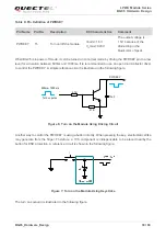
VDD_EXT 29
PO
1.8V output
power supply
for external
circuit
Vnorm=1.8V
I
O
max=50mA
Power supply for
external GPIO’s
pull-up circuits.
If unused, keep this
pin open.
GND
3, 31, 48,
50, 54, 55,
58, 59, 61,
62, 67~74,
79~82,
89~91,
100~102
Ground
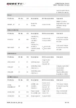
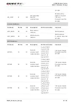
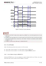
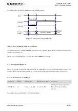
Turn on/off
Pin Name
Pin No.
I/O
Description
DC Characteristics
Comment
PWRKEY
1)
15
DI
Turn on/off the
module
Vnorm=1.5V
V
IL
max=0.45V
The output voltage is
1.5V because of the
diode drop in the
Qualcomm chipset.
PWRKEY should


