PRO-1010HD
160
1
2
3
4
1
2
3
4
C
D
F
A
B
E
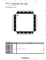
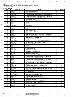
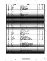
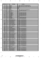
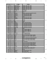
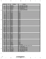
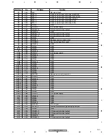
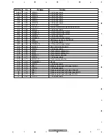
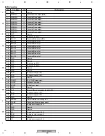
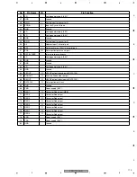
M30626FHPGP-P (DIGITAL VIDEO ASSY : IC5201)
• PDP
µ
COM
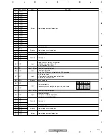
Pin Function
No.
I/0
ACTIVE
Pin Name
Function
1
VSUS
[D/A] Vofs power control
O
2
VOFS
[D/A] Vofs power control
O
3 TXD_IC4
3 serial communication with IC4MANTA - data transmission
O
4
RXD_IC4
3 serial communication with IC4MANTA - data receive
I
5
CLK_IC4
3 serial communication with IC4MANTA - clock output
O
6 BYTE
(GND
connection)
I
7
CNVSS
Pin for processor mode setting (pull-down)
I
8 NC
NC
pin
9 NC
NC
pin
10 RST_MD
Reset
input
I
L
11
XOUT
Output for main clock
O
−
12
VSS GND
−
−
13
XIN
Input for main clock
I
−
14
VCC1
Power supply = STB3.3V
−
−
15 NMI
(pull-up)
I
16 REM_B
(Interruption)
Remote control signal input (in the panel unit)
I
17
KEY_B
(Interruption) Key signal input (in the panel unit)
I
18
RST2
(Interruption) IC4 reset detection
I
L
19
HD_IN_B
HD signal existence distinction
I
L
20 PD_MUTE
Mute the power down output to the POWER SUPPLY Unit
O
L
21
PS_PD
PD signal in the POWER SUPPLY Unit
I
H
22
DCC_PD
PD signal of DC-DC converter
I
H
23 NC
NC
pin
24 NC
NC
pin
25
VD_IN
V. frequency count
I
L
26
EEPRST
EEPROM power SW
O
H
27
E_SCL
IIC clock output for EEPROM
O
28
E_SDA
IIC data I/O for EEPROM
I/O
29 TXD
Communication with flash ROM writer - data transmission
O
30
RXD
Communication with flash ROM writer - data receive
I
31
SCLK
Communication with flash ROM writer - clock input
I
32
BUSY
Communication with flash ROM writer - busy output
O
33 TXD0
UART communication with main UCOM (external PC) - data transmission
O
34 RXD0
UART communication with main UCOM (external PC) - data receive
I
35 NC
NC
pin
36
REQ_MD
Communication request to the main UCOM
O
H
37
PSW_D
Mute of DC-DC converter
O
H
38 WE_IC4
In IC4 (MANTA) rewriting, control for communication path switch
O
H
39
EPM
Setting pin for flash rewriting mode (pull-down)
I
40
IC4_RST
IC4 forced reset
O
L
41
IC4_CE
Enable for IC4 communication
O
L
42
IC4_BUSY
Busy input for IC4 communication
I
H
43
REQ_IC4
Communication request from the IC4
I
H
44
CE
Setting pin for flash rewriting mode (pull-up)
I
45
PSIZE
Panel size distinction
I
46
B_SCL
IIC clock output for backup EEPROM
O
H
47
B_SDA
IIC DATA I/O for backup EEPROM
I/O
H
48
ADR_PD
PD signal of address junction
I
H
49
LED_G
Green LED control
O
L
50
LED_R
Red LED control
O
L

