background image

PRO-1010HD

125

5

6

7

8

5

6

7

8

C

D

F

A

B

E

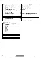
Command

Operation

Validity of 

Direct 

Numeric Input

Lower 

limit

Upper 

limit

GPM

GPD

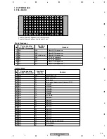
Obtaining the PULSE METER data

Obtaining the each operating information

Obtaining the power-down information

GPP

Obtaining the PD polling log for module

?

000

255

GPW

S01

S02

S03

S04

S05

S00

S01

S02

S03

S04

S10

S12

S13

S14

S15

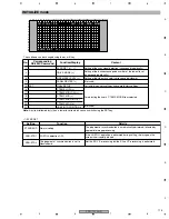
Obtaining the PANEL W/B data

GS1

GS2

Obtaining the version data for each device

GSL

Adjusting the side mask GREEN

GYG

Adjusting the GY GAIN

[I]

INP

Indicating the input function of current main screen

INP

Switching the main screen to Input 1

INP

Switching the main screen to Input 2

INP

Switching the main screen to Input 3

INP

Switching the main screen to Input 4

Switching the main screen to Input 5

?

000

255

INP

[M]

MSK

White: 0 to 100%

MSK

Mask mode: OFF

MSK

Aging mask (detection of still picture: OFF)

MSK

Aging mask

MSK

Aging mask (detection of still picture: OFF)

MSK

S11

MSK

RAMP slant 1

RAMP slant 4

MSK

RAMP slant 1 shifting

MSK

RAMP slant 4 shifting

MSK

V RAMP

MSK

S20

S21

S22

S23

S24

S25

S26

S27

S28

S29

S40

S30

S31

S51

MSK

H/V RAMP

Window (for W/B adjustment   High: 870, Low: 102)

MSK

Window (for W/B adjustment   High: 1023, Low: 102)

MSK

Window (for the peak luminance measurement of WB stage   High: 1023)

MSK

Window (for the peak luminance measurement   High: 1023  4%)

MSK

Window (for the peak luminance measurement   High: 1023  1.25%)

MSK

Window-1/7 vertical window (for stress measurement)

MSK

Window (magenta, green, stripe for checker)

MSK

Window (green, magenta, stripe for checker)

MSK

Window (black & white [1 x 8], checkered pattern [for EMG check])

MSK

Window (for W/B adjustment, magenta=512, yellow=512)

MSK

Wiper to prevent phosphor burn

MSK

Color Bar

MSK

Slanted lines (breaking of wire check)

MSK

S52

S53

S54

S55

S56

S57

S58

S59

MSK

Raster-white

Raster-red

MSK

Raster-green

MSK

Raster-blue

MSK

Raster-black

MSK

Raster-cyan

MSK

Raster-magenta

MSK

Raster-yellow

MSK

Raster-cyan 274

Содержание Elite PRO-1010HD

Страница 1: ...9936 PIONEER CORPORATION 2004 PRO 1010HD ARP3219 PLASMA DISPLAY PRO 1010HD PRO 810HD THIS MANUAL IS APPLICABLE TO THE FOLLOWING MODEL S AND TYPE S This service manual should be used together with the following manual s Model Type Power Requirement Remarks PRO 1010HD KUCXC AC120V PRO 810HD KUCXC AC120V Model No Order No Remarks PRO 1010HD PRO 810HD ARP3220 SCHEMATIC DIAGRAM PCB CONNECTION DIAGRAM F...

Страница 2: ... adjustment and compartment covershields isolation resistor capacitor etc 3 When service is required observe the original lead dress Extra precaution should be taken to assure correct lead dress in the high voltage circuitry area 4 Always use the manufacture s replacement components Especially critical components as indicated on the circuit diagram should not be replaced by other manufacture s Fur...

Страница 3: ...c Any current measured must not exceed 0 5mA ANY MEASUREMENTS NOT WITHIN THE LIMITS OUTLINED ABOVE ARE INDICATIVE OF A POTENTIAL SHOCK HAZARD AND MUST BE CORRECTED BEFORE RETURNING THE SET TO THE CUSTOMER PRODUCT SAFETY NOTICE Many electrical and mechanical parts in PIONEER set have special safety related characteristics These are often not evident from visual inspection nor the protection afforde...

Страница 4: ...nsformer and Converter Transformer In the POWER SUPPLY Unit 6 Other primary side of the POWER SUPPLY Unit High Voltage Generating Point The places where voltage is 100V or more except for the charged places described above If the places are touched there is a risk of electric shock 1 POWER SUPPLY Unit 223V 2 50 X DRIVE Assy 230V to 223V 3 50 Y DRIVE Assy 353V 4 50 SCAN A Assy 353V 5 50 SCAN B Assy...

Страница 5: ...ransformer and Converter Transformer In the POWER SUPPLY Unit 6 Other primary side of the POWER SUPPLY Unit Part is the High Voltage Generating Points other than the Charged Section Part is Charged Section For PRO 810HD Fig 2 Charged Section and High Voltage Generating Point Rear View AC Inlet with Filter Power Cord Power Switch S1 POWER SUPPLY Unit 43 SCAN B Assy 43 Y DRIVE Assy 43 SCAN A Assy X ...

Страница 6: ... the product Please check that neither solder debris nor screws remain inside the product 8 There should be no semi broken wires scratches melting etc on the coating of the power cord Damaged power cords may lead to fire accidents so please be sure that there are no damages If you find a damaged power cord please exchange it with a suitable one 9 There should be no spark traces or similar marks on...

Страница 7: ... for PRO 810HD model 44 3 1 3 OVERALL BLOCK DIAGRAM 2 2 for PRO 1010HD and PRO 810HD models 46 3 1 4 SIGNAL ROUTE 48 3 1 5 50 Y DRIVE ASSY 49 3 1 6 43 Y DRIVE ASSY 50 3 1 7 50 X DRIVE ASSY 51 3 1 8 43 X DRIVE ASSY 52 3 1 9 DIGITAL VIDEO ASSY 53 3 1 10 AV I O ASSY 54 3 1 11 RGB ASSY 55 3 1 12 AUDIO AMP and COMM SLOT ASSYS 56 3 1 13 VIDEO SLOT 1 ASSY 57 3 2 WAVEFORMS 58 3 3 VOLTAGES 65 4 PCB CONNECT...

Страница 8: ...tible RGB 0 7 Vp p 75 no sync HD CS VD TTL level positive and negative polarity 2 2 k G ON SYNC 1 Vp p 75 negative sync Compatible with Microsoft Plug Play VESA DDC1 2B Component video signal Y 1 Vp p 75 negative sync CB PB CR PR 0 7 Vp p color100 75 HDMI Digital signal 3 3V T M D S 50 INPUT2 Input HDMI Digital signal 3 3V T M D S 50 INPUT3 Input S jack Mini DIN 4 pin Y C separate video signal Y 1...

Страница 9: ...0HD 9 5 6 7 8 5 6 7 8 C D F A B E Accessories Power Cord ADG1215 Remote Control Unit AXD1496 Binder Assy AEC1758 Dry Cell Battery R6P AA Cleaning Cloth for wiping front panel AED1208 Speed Clamp 2 Bead Bands 2 ...

Страница 10: ...on some component parts indicates the importance of the safety factor of the part Therefore when replacing be sure to use parts of identical designation Screws adjacent to mark on product are used for disassembly For the applying amount of lubricants or glue follow the instructions in this manual In the case of no amount instructions apply as you think it appropriate NOTES 18 17 16 16 1 17 11 12 1...

Страница 11: ... Operating Instructions ARE1385 English French Spanish 8 Plasma Caution Sheet ARM1145 9 Caution Sheet ARM1176 10 Caution Sheet ARM1194 11 Caution Sheet ARM1201 12 Mirror Mat AHG1284 NSP 13 Warranty Card EL ARY1123 NSP 14 Card VRY1132 15 Vinyl Bag AHG1310 16 Pad AHA2385 17 Under Carton See Contrast table 2 18 Upper Carton See Contrast table 2 19 Front Sheet See Contrast table 2 20 Accessory Case AH...

Страница 12: ...C D F A B E 2 2 PRO 1010HD model 2 2 1 CHASSIS SECTION 1 2 22 22 22 2 22 22 22 10 5 12 4 8 14 20 21 19 21 15 15 17 17 17 17 17 17 18 24 18 17 15 15 15 15 15 15 15 1 23 3 6 14 14 14 7 9 14 11 14 14 14 14 14 13 18 15 15 15 16 16 15 25 ...

Страница 13: ...exible Cable J209 ADD1236 9 Flexible Cable J210 ADD1237 10 Flexible Cable J205 ADD1252 11 Flexible Cable J206 ADD1253 12 Flexible Cable J207 ADD1254 13 Flexible Cable J208 ADD1255 14 Flat Clamp AEC1879 15 PCB Spacer AEC1941 16 PCB Support AEC1938 17 Wire Saddle AEC1745 18 PCB Spacer AEC1947 19 Locking Wire Saddle AEC1948 20 Drive Silicone Sheet C AEH1066 21 Drive Silicone Sheet B AEH1065 22 Screw ...

Страница 14: ...F A B E 2 2 2 CHASSIS SECTION 2 100V 8 20 20 15 18 17 16 4 5 16 1 17 17 18 18 17 16 16 2 7 11 12 6 16 16 16 17 17 15 15 13 17 26 28 27 15 14 15 15 15 15 15 19 9 10 19 15 24 23 22 25 3 Upper side Upper side 21 21 21 21 21 21 21 21 21 21 ...

Страница 15: ...9 Fan Motor 80 x 25 AXM1044 10 Fan Angle 504 ANG2609 11 Front Chassis VL 50M ANA1753 12 Front Chassis VR 50M ANA1754 13 SCAN Heatsink ANH1630 14 Housing Wire J117 ADX2897 15 Screw ABZ30P060FMC 16 Screw PMB30P060FNI 17 Screw VBB30P080FNI 18 Screw PMB40P080FZK 19 Screw PPZ50P100FZK 20 Nylon Rivet AEC1671 21 Screw AMZ30P060FZK 22 3P Housing Wire J109 ADX2847 23 11P Housing Wire J102 ADX2853 24 12P Ho...

Страница 16: ... F A B E 2 2 3 FRAME SECTION 17 17 6 16 9 9 5 4 16 16 19 16 Upper side 7 7 7 7 7 7 17 16 18 16 18 11 10 11 2 13 23 12 1 14 14 3 15 20 21 11 25 24 11 8 17 7 6 7 7 7 7 7 17 17 17 17 17 17 17 18 18 18 17 16 16 19 18 17 17 17 8 17 17 17 22 ...

Страница 17: ...MX AMR3384 8 Rear Frame 50M ANG2602 9 Locking Wire Saddle AEC1948 10 Locking Wire Saddle AEC1992 11 Wire Saddle AEC1745 NSP 12 IR Holder ANG2551 13 Nylon Rivet AEC1671 14 Flat Clamp AEC1879 15 Enclosure Sheet 1 AMR3405 16 Screw AMZ30P080FMC 17 Screw AMZ30P060FZK 18 Screw APZ30P080FZK 19 Screw ABZ30P060FMC 20 Nylon Rivet AEC1997 21 Screw BBZ30P050FMC 22 Enclosure Sheet 2 V AMR3411 23 Enclosure Shee...

Страница 18: ...6 18 30 4 18 18 8 1 7 8 17 17 8 9 2 38 38 20 17 37 38 25 18 5 6 6 25 18 18 18 23 24 18 18 18 18 18 30 18 14 14 13 13 39 11 10 11 3 22 21 17 19 19 30 30 30 18 18 18 18 18 18 18 18 18 18 18 18 28 29 27 33 34 35 12 32 32 31 18 18 18 26 18 18 30 30 30 32 32 31 36 1 4 36 3 4 36 2 4 36 4 4 Default 2 2kΩ ...

Страница 19: ...pring T130 ABK1032 15 Slot Spring T94 ABK1034 16 Slot Spring B92 ABK1035 17 Screw VBB30P080FNI 18 Screw AMZ30P060FZK 19 Screw BMZ30P080FZK 20 Hexagon Head Screw BBA1051 21 Power Switch S1 ASG1094 22 Housing Wire MX J116 ADX2896 23 COMM Stay A ANG2605 24 COMM Stay B ANG2606 25 Screw APZ30P080FZK 26 Rear Case 50M ANE1623 27 Gasket T R50 ANK1735 NSP 28 Name Label E50J AAL2589 29 Caution Label AAX3048...

Страница 20: ...PRO 1010HD 20 1 2 3 4 1 2 3 4 C D F A B E 2 2 5 FRONT SECTION 1 4 3 5 6 3 6 6 8 6 6 6 4 14 14 14 14 13 13 15 10 18 1 16 17 11 12 ...

Страница 21: ...V AED1199 4 Panel Cushion H AED1226 5 Protect Panel Assy 50 AMR3348 6 Panel Holder 50 ANG2563 7 8 Front Case Assy E50 AMB2842 9 10 Blind Cushion AEB1400 11 Flexible Cable J211 ADD1265 12 Flexible Seal AEH1074 13 Screw ABZ30P060FMC 14 Screw APZ30P080FZK 15 Screw APZ30P120FZK 16 Lead Cover E AMR3435 17 Rivet AEC1877 18 Earth Plate MX AMR3432 ...

Страница 22: ...ECTION 2 Rear view Rear view 10 11 13 18 19 Front side 16 15 21 21 1 1 12 17 1 1 21 21 21 21 21 8 6 21 21 21 21 6 4 7 21 21 7 21 21 21 21 7 3 21 21 21 21 21 21 6 9 21 21 21 7 3 21 6 21 21 21 22 20 22 20 22 20 22 20 14 14 14 14 21 2 5 23 2 5 23 2 5 23 2 5 23 ...

Страница 23: ...2696 6 Fixing Plate 50 ANG2697 7 Fixing Plate 50S ANG2707 8 Coner Plate 43DL ANG2709 9 EMC Plate ANG2711 10 LED Lens E AAK2832 11 IR Lens E AAK2833 12 Side Spacer A E AMR3437 13 Side Spacer B E AMR3438 14 Gasket E ANK1746 15 Frame U E50 ANB1871 16 Frame L E50 ANB1872 17 Frame R E50 ANB1873 18 Frame D E50 ANB1874 19 ELITE Badge AAM1102 20 Spring Washer WS80FZK 21 Screw A ABA1304 22 Screw B ABA1305 ...

Страница 24: ... NSP Plasma Panel Assy 50 V1 AAV1251 NSP FPC 50XGA X ADY1084 NSP FPC 50XGA Y ADY1085 NSP Chassis Assy 50 ANA1774 Edge Card Spacer AEC1998 PCB Spacer AEC1944 PCB Support AEC1958 Rivet AMR1066 FC Spacer AMR3370 NSP Adhesive ZBA KE3424S NSP Cleaner ZLX AP7 NSP Tape ZTA 8101 12 NSP Double Faced Tape ZTB 5015 18 NSP Tape ZTC POLYCA 11 NSP Tape ZTC POLYCA 20 NSP Double Faced Tape ZTB 5015 9 NSP Tape ZTC...

Страница 25: ...ort AEC1938 PCB Spacer AEC1941 PCB Spacer AEC1947 Wire Clip AEC1948 Wire Clip AEC1992 Panel Cushion V AED1199 Panel Cushion H AED1226 Siricon Sheet SC AEH1080 Front Spacer AMR3369 Caution Label AAX3031 NSP Drive Voltage Label ARW1097 Screw ABZ30P100FZK Screw AMZ30P060FZK Screw AMZ30P080FMC Screw APZ30P080FZK NSP Front Case 504 SVC AMB2811 Rear Case 50P ANE1614 Caution Card SVC ARM1247 Pad PP T L A...

Страница 26: ... 3 1 CHASSIS SECTION 1 2 1 27 27 24 25 25 24 2 20 21 21 21 21 17 16 16 16 16 16 18 18 18 17 17 16 17 17 17 19 18 18 19 23 22 20 20 22 20 27 27 16 16 20 5 8 4 14 14 14 12 13 14 11 15 15 15 15 10 14 14 28 14 14 6 7 9 15 15 26 3 21 20 20 21 16 22 16 31 29 31 31 31 30 ...

Страница 27: ... ADD1261 11 Flexible Cable J206 ADD1262 12 Flexible Cable J207 ADD1263 13 Flexible Cable J208 ADD1264 14 Ferrite Core ATX1048 15 Flat Clamp AEC1879 16 PCB Spacer AEC1941 17 PCB Support AEC1938 18 PCB Spacer AEC1944 19 PCB Support AEC1958 20 Ferrite Clamp AEC1986 21 Wire Saddle AEC1745 22 PCB Spacer AEC1947 23 Locking Wire Saddle AEC1948 24 Drive Silicone Sheet C AEH1066 25 Drive Silicone Sheet B A...

Страница 28: ... SECTION 2 100V 8 20 20 4 5 1 18 18 18 17 17 17 17 2 12 13 7 6 16 16 16 16 17 17 15 15 24 15 22 25 23 29 30 15 28 26 27 15 15 15 9 11 19 19 14 15 15 15 9 10 19 19 3 Upper side Upper side Upper side Upper side 21 21 21 21 21 21 21 21 21 21 31 31 31 31 32 32 ...

Страница 29: ...le R 43M ANG2656 12 Front Chassis VL 43M ANA1755 13 Front Chassis VR 43M ANA1756 14 Housing Wire for Fan J117 ADX2904 15 Screw ABZ30P060FMC 16 Screw PMB30P060FNI 17 Screw VBB30P080FNI 18 Screw PMB40P080FZK 19 Screw PPZ50P100FZK 20 Nyron Rivet AEC1671 21 Screw AMZ30P060FZK 22 3P Housing Wire J109 ADX2847 23 11P Housing Wire J102 ADX2840 24 12P Housing Wire J103 ADX2841 25 Wire A J101 ADX2839 26 Wir...

Страница 30: ...1 2 3 4 C D F A B E 2 3 3 FRAME SECTION 19 Upper side 9 10 17 24 17 24 16 16 17 24 18 18 6 6 8 4 5 7 7 7 7 7 7 7 7 7 7 7 7 18 24 16 16 17 17 17 17 17 17 11 11 2 13 22 23 12 1 14 14 3 20 15 21 19 Rear view Rear view 26 25 10 ...

Страница 31: ...384 8 Rear Frame 43M ANG2613 9 Locking Wire Saddle AEC1948 10 Locking Wire Saddle AEC1992 11 Wire Saddle AEC1745 NSP 12 IR Holder ANG2551 13 Nyron Rivet AEC1671 14 Flat Clamp AEC1879 15 Enclosure Sheet 1 AMR3405 16 Screw AMZ30P080FMC 17 Screw AMZ30P060FZK 18 Screw APZ30P080FZK 19 Screw ABZ30P060FMC 20 Nyron Rivet AEC1997 21 Screw BBZ30P050FMC 22 Enclosure Sheet 2 V AMR3411 23 Enclosure Sheet 3 AMR...

Страница 32: ... 30 4 18 18 8 1 7 8 17 17 8 9 2 39 39 20 17 38 39 25 18 5 6 6 25 18 18 18 23 24 18 18 18 18 18 18 18 30 37 37 37 37 13 13 14 14 11 10 11 3 22 21 17 19 19 30 30 30 18 18 18 18 18 18 18 18 18 18 18 18 28 29 27 33 34 35 32 32 31 18 18 26 18 18 30 30 30 32 32 31 36 1 4 36 3 4 36 2 4 36 4 4 12 Default 2 2kΩ ...

Страница 33: ...T130 ABK1032 15 Slot Spring T94 ABK1034 16 Slot Spring B92 ABK1035 17 Screw VBB30P080FNI 18 Screw AMZ30P060FZK 19 Screw BMZ30P080FZK 20 Hexagon Head Screw BBA1051 21 Power Switch S1 ASG1094 22 Housing Wire MX J116 ADX2896 23 COMM Stay A ANG2605 24 COMM Stay B ANG2606 25 Screw APZ30P080FZK 26 Rear Case 43M ANE1624 27 Gasket T R43 ANK1736 NSP 28 Name Label E43J AAL2592 29 Caution Label M AAX3048 30 ...

Страница 34: ...PRO 1010HD 34 1 2 3 4 1 2 3 4 C D F A B E 2 3 5 FRONT SECTION 1 4 3 3 8 4 15 5 6 6 6 6 6 6 14 14 14 13 13 14 10 18 1 16 17 11 12 ...

Страница 35: ...AED1254 4 Panel Cushion H 43M AED1253 5 Protect Panel Assy 43 AMR3345 NSP 6 Panel Holder 43 ANG2552 7 8 Front Case Assy E43 AMB2845 9 10 Blind Cushion AEB1400 11 Flexible Cable J211 ADD1265 12 Flexible Seal AEH1074 13 Screw ABZ30P060FMC 14 Screw APZ30P080FZK 15 Screw APZ30P120FZK 16 Lead Cover E AMR3435 17 Rivet AEC1877 18 Earth Plate MX AMR3432 ...

Страница 36: ... 3 4 C D F A B E 2 3 6 FRONT SECTION 2 Rear view Rear view 10 11 13 18 16 15 21 21 1 1 12 17 1 1 21 8 21 21 4 21 21 7 21 21 21 21 7 6 21 21 21 21 21 21 7 3 21 19 Front side 22 20 22 20 22 20 22 20 2 5 23 2 5 23 2 5 23 2 5 23 14 ...

Страница 37: ...e LD ANG2696 6 Coner Plate 43UL ANG2708 7 Fixing Plate 50S ANG2707 8 Coner Plate 43DL ANG2709 9 10 LED Lens E AAK2832 11 IR Lens E AAK2833 12 Side Spacer A E AMR3437 13 Side Spacer B E AMR3438 14 Gasket 2 E ANK1747 15 Frame U E43 ANB1875 16 Frame L E43 ANB1876 17 Frame R E43 ANB1877 18 Frame D E43 ANB1878 19 ELITE Badge AAM1102 20 Spring Washer WS80FZK 21 Screw A ABA1304 22 Screw B ABA1305 23 Scre...

Страница 38: ...XF1124 NSP Plasma Panel Assy 43 V1 AAV1250 NSP FPC 43XGA X ADY1079 NSP FPC 43XGA Y ADY1080 NSP Chassis Assy 43 ANA1773 PCB Spacer AEC1944 PCB Support AEC1958 Edge Card Spacer AEC1998 Rivet AMR1066 FC Spacer AMR3370 NSP Adhesive ZBA KE3424S NSP Cleaner ZLX AP7 NSP Tape ZTA 8101 12 NSP Double Faced Tape ZTB 5015 18 NSP Double Faced Tape ZTB 5015 9 NSP Tape ZTC POLYCA 11 NSP Tape ZTC POLYCA 20 NSP Ta...

Страница 39: ...B Spacer AEC1947 Locking Wire Saddle AEC1948 HL18 AEC1980 Ferrite Clamp AEC1986 Locking Wire Saddle AEC1992 Panel Cushion H 43M AED1253 Panel Cushion V 43M AED1254 Front Spacer CMX AMR3384 Y Drive Protection Sheet AMR3346 Front Spacer AMR3369 Caution Label AAX3031 NSP Drive Voltage Label ARW1097 Screw ABZ30P100FZK Screw AMZ30P060FZK Screw AMZ30P080FMC Screw APZ30P080FZK Screw VBB30P080FNI NSP Fron...

Страница 40: ... PRO 810HD models 2 4 1 MULTI BASE SECTION Note This illustration is PRO 1010HD Bottom view Rear view 34 28 28 11 11 10 10 10 7 7 7 7 7 7 7 7 7 8 11 11 12 14 14 26 23 15 15 21 22 20 26 3 27 30 30 30 25 24 25 27 28 28 28 19 32 18 13 12 13 29 29 16 6 9 9 33 23 33 28 31 29 17 13 5 4 2 1 ...

Страница 41: ...Double Locking Spacer AEC1988 16 15P 16P Housing Wire J106 ADX3028 17 Cable Clamp AEC1707 18 10 11P Housing Wire J110 See Contrast table 2 19 10P Housing Wire J113 ADX2908 20 12P Housing Wire J112 ADX2892 21 13P 6P Housing Wire J104 ADX2910 22 COVER Assy AWZ6858 23 Guide Rail EX AEC1994 24 Slot Stay ANG2608 25 Wire Saddle AEC1745 26 11P Housing Wire J111 See Contrast table 2 27 Flat Clamp AEC1879 ...

Страница 42: ... IC5V ADD SEL_PULSE IC3205 VCC _VH IC5V ADD SEL_PULSE IC3206 DRIVER IC IC1552 DRIVER IC IC1553 DRIVER IC IC1554 IC1501 RESONANCE BLOCK DRIVER IC IC1555 V 5V V 9V V ADR V 3V_IC5 V 3V_PLL V 3V_LVDS V 60V DRIVER IC IC1551 CN1501 AD1 50 ADDRESS ASSY V ADR DRIVER IC IC1552 DRIVER IC IC1553 DRIVER IC IC1554 IC1501 RESONANCE BLOCK DRIVER IC IC1555 V 5V V 9V V 3V_IC5 V 3V_PLL V 3V_LVDS V 60V DRIVER IC IC1...

Страница 43: ...IC1552 DRIVER IC IC1553 DRIVER IC IC1554 IC1501 RESONANCE BLOCK DRIVER IC IC1555 V 5V V 9V V ADR V 3V_IC5 V 3V_PLL V 3V_LVDS V 60V DRIVER IC IC1551 CN1501 AD1 50 ADDRESS ASSY X1 X2 X CONNECTOR B ASSY X CONNECTOR A ASSY SP TERMINAL L ASSY 50 X DRIVE ASSY 5V 5V 5V Drive Signal Drive Signal 16 5V 16 5V 16 5V VSUS V_RN 5V 6 5V V_RN MASK MOD IC1203 5V 16 5V VSUS MASK MOD IC1207 REGULATOR DC_DC CONV BLO...

Страница 44: ...C _VH IC5V ADD SEL_PULSE IC3205 VCC _VH IC5V ADD SEL_PULSE IC3206 DRIVER IC IC1552 DRIVER IC IC1553 DRIVER IC IC1554 IC1501 RESONANCE BLOCK DRIVER IC IC1555 V 5V V 9V V ADR V 3V_IC5 V 3V_PLL V 3V_LVDS V 60V CN1501 AD1 43 ADDRESS ASSY V ADR DRIVER IC IC1552 DRIVER IC IC1553 DRIVER IC IC1554 IC1501 RESONANCE BLOCK DRIVER IC IC1555 V 5V V 9V V 3V_IC5 V 3V_PLL V 3V_LVDS V 60V CN1501 AD1 43 ADDRESS ASS...

Страница 45: ...IC1553 DRIVER IC IC1554 IC1501 RESONANCE BLOCK DRIVER IC IC1555 V 5V V 9V V ADR V 3V_IC5 V 3V_PLL V 3V_LVDS V 60V CN1501 AD1 43 ADDRESS ASSY X1 X2 X CONNECTOR B ASSY X CONNECTOR A ASSY 43 X DRIVE ASSY 5V 5V 5V Drive Signal Drive Signal 16 5V 16 5V 16 5V VSUS V_RN 5V 6 5V V_RN MASK MOD IC1203 5V 16 5V VSUS MASK MOD IC1207 REGULATOR DC_DC CONV BLOCK LOGIC BLOCK RESONANCE BLOCK RESET PULSE BLOCK PSUS...

Страница 46: ...SSY VIDEO SLOT I F ASSY COMM SLOT I F ASSY IR RECEIVE ASSY AUDIO AMP ASSY R R L L R R V 12V V 3V V 3 3V_STB V 6 5V V 13V V 12V V 3V V 16 IC7606 IC7607 INPUT 3 4 INPUT 5 Y Cb Cr H V CLK DE Y Cb Cr H V CLK DE CN7601 AV4 CS5 CS1 VS2 VS4 VS3 VS1 VS5 CN7605 AV3 CN8703 CN9651 AV2 KY1 LO1 CN8702 AV5 AV6 RE1 CS2 CS4 CS3 CN8704 CN8905 CN8901 CN4901 CN8903 CN8902 CN9454 CN7902 CN8954 CN8904 CN2101 CN2102 CN...

Страница 47: ...SELECTOR LPF IC7207 MAIN UCOM IC6603 SELECTOR IC7201 IC7204 SELECTOR RGB H V RGB H V H V H V H V H V H V H V H V H V H V RGB RGB C SYNC G ON SYNC RGB H V H V H V H V H V H V RGB RGB TRAP_SW FAN_12V TXD_MD RXD_MD RGB V 1V _DD V 3V _DD V 6 5V V 3V _STB V 16 5V R12 R3 R13 R2 R9 R11 R4 CN7402 CN7204 CN5801 CN6401 CN6402 R10 R8 R6 CN7404 CN7408 R5 R1 CN7101 CN7406 CN5701 CN9702 D3 CN5002 D15 CN5001 P8 ...

Страница 48: ... 64M 2 FLASH ROM 32M Y X 2 Divide SW PD6435A IC5801 Y X 2 Divide SW 74VHC125 SM5301BS LPF SM5301BS LPF A D PLL BA7078AF COMPOSITE SYNC COMPOSITE SYNC G ON SYNC G ON SYNC H V 74HC125 74VHC125 5 3 3V 5 3 3V SYNC SEP BA7078 SYNC SEP IC6002 AD9883AKST A D PLL 2 1 2 1 SYNC PROCESS SYNC PROCESS MANTA VIDEO PROCESS MULTI PROCESS IP IP FRC NR LVDS Sequence IC7004 PE5362A 48bit DUAL R G B X 8bit X2 H V CLK...

Страница 49: ...FS YSUS MSK YOFS YSUS PD SCN_5V_PD Y_DD_PD SCAN_PD YDRIVE_PD 16 5V DGND 6 5V DGND N C N C VSUS VSUS VSUS VH OVP VOFS UVP VH UVP VSUS N C SUSGND SUSGND VH 5V VSUS VH IC5V CN2101 CN2102 IC2305 5V IC5V VH VF Y2 Y3 Y1 VOFS OVP VOFS IC5V UVP VF IC2201 L2202 L2203 YSUS U2 YSUS D2 HB DRIVER XSUS P D Circuit Photo Coupler 5V VSUS To SCAN ASSY To 50 SCAN B ASSY From DIGITAL VIDEO ASSY From POWER SUPPLY UNI...

Страница 50: ...FS YSUS MSK YOFS YSUS PD SCN_5V_PD Y_DD_PD SCAN_PD YDRIVE_PD 16 5V DGND 6 5V DGND N C N C VSUS VSUS VSUS VH OVP VOFS UVP VH UVP VSUS N C SUSGND SUSGND VH 5V VSUS VH IC5V CN2101 CN2102 IC2305 5V IC5V VH VF Y2 Y3 Y1 VOFS OVP VOFS IC5V UVP VF IC2201 L2202 L2203 YSUS U2 YSUS D2 HB DRIVER XSUS P D Circuit Photo Coupler 5V VSUS To SCAN ASSY To 43 SCAN B ASSY From DIGITAL VIDEO ASSY From POWER SUPPLY UNI...

Страница 51: ... XNR D XNR D XSUS_PD XDD_PD XDRV_PD 16 5V DGND 6 5V DGND N C N C VSUS VSUS VSUS VRN UVP P D VRN OVP P D VSUS N C SUSGND SUSGND 5V CN1201 IC1205 5V X1 X2 N C IC1101 L1102 L1103 XSUS U2 XSUS D2 HB DRIVER XSUS P D Circuit Photo Coupler 5V VCP VSUS PSUS To X CONNECTOR ASSY From DIGITAL VIDEO ASSY From POWER SUPPLY UNIT 5V 16 5V VSUS 5V 16 5V IC1102 IC1202 Charge Pump Circuit XNR P D DET D D CONV T1401...

Страница 52: ... XNR D XNR D XSUS_PD XDD_PD XDRV_PD 16 5V DGND 6 5V DGND N C N C VSUS VSUS VSUS VRN UVP P D VRN OVP P D VSUS N C SUSGND SUSGND 5V CN1201 IC1205 5V X1 X2 N C IC1101 L1102 L1103 XSUS U2 XSUS D2 HB DRIVER XSUS P D Circuit Photo Coupler 5V VCP VSUS PSUS To X CONNECTOR ASSY From DIGITAL VIDEO ASSY From POWER SUPPLY UNIT 5V 16 5V VSUS 5V 16 5V IC1102 IC1202 Charge Pump Circuit XNR P D DET D D CONV T1401...

Страница 53: ...AN_ PD YDRV_ PD YRES_ PD YDC_ PD IC5V_ PD XSUS_ PD XDC_ PD XDRV_ PD PS_ PD DCC_ PD DVI_ MUTE Xtal Xtal AND BUSY RXD1 CLK1 CNVSS TXD1 PANEL SIZE PSIZE Vofs YDRV_ UC XDRV_ UC AC_ DET EMG Det STB_ MT Excepting panel module Video signal Sync signal IIC communication 3 wire serial down Others MRAC_ DET B_ SCL B_ SDA VOFS VSUS VD_ IN PSW _ D EMG DIGITAL VIDEO ASSY IC5201 HD VD CLK DE Works by passive st...

Страница 54: ...A6801 INPUT1 HDMI JA6802 INPUT2 HDMI JA7601 INPUT1 AUDIO JA7602 INPUT2 AUDIO IC7611 H V H V Digital Video Analog Video Digital Video TMDS Transmission Digital Audio Analog Audio ANA_SW HDMI_MUTE SCL_AV SDA_AV HDMI_AUDIO_TXD RXD CE D_AUDIO_SEL L R SLOT L R HDMI_AUDIO HDMI2_SCL HDMI2_SDA Y Cb Cr 8bit CLK H V DE SCL_AV SDA_AV A_SW0 A_SW1 L R Y Cb Cr R G B Y Cb Cr R G B Y Cb Cr BUFFER BUFFER IC7606 IC...

Страница 55: ... 48bit DUAL R G B X 8bit X2 H V CLK DE RGB ASSY ANALOG SYNC IC7101 PD5855A WIRED OR R10 CN7101 IC7402 MM1522XU CN7406 IC7401 IC7206 R6 CN7204 R3 CN7402 R8 CN7407 R4 CN7408 R5 CN7404 R1 R2 CN6401 IC6402 AN5870SB R13 CN6402 R12 CN7405 R11 CN7410 BUFFER IC6404 IC7001 TXD_MD RXD_MD UART_TXD UART_RXD EEP ROM IC7102 SDRAM 64M IC7002 X7001 OSC X7201 IC7151 IC7207 MAIN UCOM TEMP2 TEMP3 IC7404 FAN CONT FAN...

Страница 56: ...9454 1 pin IC9454 2 pin IC9455 2 pin IC9456 4 pin IC9456 3 pin IC9452 2 pin IC9452 3 pin IC9457 2 pin IC9457 1 pin L L DC DETECT DD CONVERTER R R L_OUT L_OUT R_OUT R_OUT TEMP3 FIRST RXD RXD_CARD UART_SW SR IN SR OUT TXD_PDP TXD_CARD RXD_PDP INT_EXT GET_UART V 16 5 TEMP3 JA9453 232C JA9451 SR TXD TXD T2 IN R2 OUT RXD RXD A_NG AMUTE STBY V 12V V 6 5V V 3 3V V 3 3V V 12V_D AP3 CN5003 AP1 CN5002 CN945...

Страница 57: ...106 IC42S16100 7TG K LPF Xtal IC1 Y C BLOCK IC1 CVBS BLOCK INPUT REG BLOCK SIGNAL SW BLOCK Discrete 16MHz LPF V V V Discrete 16MHz 27MHz CLK ADD SLOT ANALOG SLOT To CN8954 184pin DIGITAL SLOT VIDEO SLOT1 ASSY IC7802 TK15420 INPUT4 SIGNAL DETECTION Regulator HV HV HV HV RGB or YCbCr Y C HV Control Signal IN4_DET Control Signal Control Signal YCbCr YCbCr WIRED OR Audio L R Audio L R INPUT 5 INPUT 3 ...

Страница 58: ...1 CH2 2 CH1 K5003 VD CH2 K5004 DE V 2V div H 2msec div CH1 CH2 2 CH1 K5003 VD CH2 K5004 DE V 2V div H 4µsec div CH1 CH2 3 CH1 K5002 HD CH2 K5004 DE V 2V div H 2µsec div CH1 CH2 3 CH1 K5002 HD CH2 K5004 DE V 2V div H 40nsec div CH1 CH2 4 CH1 K5002 HD CH2 CN5001 pin 77 DCLK V 2V div H 40nsec div CH1 CH2 5 CH1 K5003 VD CH2 CN5001 pin 88 RA_IN2 V 2V div H 2msec div CH1 CH2 DIGITAL I F BLOCK ...

Страница 59: ...HD_SUB V 2V div H 4µsec div CH2 Foot of C6614 GAIN V 200mV div H 4µsec div 11 9 CH1 IK6012 PLLHD_MAIN V 2V div H 4µsec div CH2 K6013 CLAMP_MAIN V 2V div H 4µsec div 19 21 CH1 Foot of R6628 DATACK V 2V div H 10nsec div CH2 Foot of R6644 RED0 V 2V div H 10nsec div 22 23 CH1 IC6008 pin2 CLK V 2V div H 20nsec div CH2 IC6006 pin 9 RB0 V 2V div H 20nsec div 24 16 CH1 K6601 PLLHD_SUB V 2V div H 4µsec div...

Страница 60: ...LSINI1 V 1V div H 100msec div IC6107 pin 90 PLSINI2 V 200mV div H 20µsec div IC6107 pin 67 Y V 1V div H 4msec div IC6107 pin 107 VD_IC1V 3 4 V 200mV div H 20µsec div Q6257 2 2 Emitter YIN 9 5 10 15 17 11 13 6 7 8 12 IC6255 pin 67 Y V 200mV div H 20µsec div IC6255 pin 87 PLSINI1 V 1V div H 100nsec div IC6255 pin 72 Cb V 200mV div H 20µsec div 14 IC6255 pin 108 HD_IC1S V 1V div H 20µsec div 16 IC625...

Страница 61: ... V 2V div H 5µsec div CH2 CN7605 pin 12 B_IO V 500mV div H 5µsec div 6 7 CH1 JA7606 pin 13 HD V 2V div H 5µsec div CH2 JA7606 pin 1 R V 500mV div H 5µsec div CH1 CH2 1 2 CH1 CN7605 pin 10 HD_IO V 2V div H 10µsec div CH2 CN7605 pin 16 R_IO V 500mV div H 10µsec div CH1 CH2 6 8 CH1 JA7606 pin 13 HD V 2V div H 5µsec div CH2 JA7606 pin 2 G V 500mV div H 5µsec div CH1 CH2 6 9 CH1 JA7606 pin 13 HD V 2V d...

Страница 62: ...0µsec div CH2 CN5003 pin 8 L V 2V div H 500µsec div CH1 CH2 13 14 CH1 CN7601 pin 14 L_OUT V 200mV div H 500µsec div CH2 CN7601 pin 13 L_OUT V 200mV div H 500µsec div CH1 CH2 AUDIO AMP ASSY AUDIO Input INPUT 1 Signal 200mVrms 1 kHz input VOL MAX AV IO BLOCK COMM SLOT 1 ASSY SR waveforms when Volume is upped AUDIO Input INPUT 1 Signal 200mVrms 1 kHz input VOL MAX 1 CN9454 pin 106 RXD_PDP V 2V div H ...

Страница 63: ...US U1 K2010 DGND CH4 K2022 YSUS U2 K2010 DGND CH5 K2026 YSUS B K2010 DGND CH6 K2024 YSUS D2 K2010 DGND CH7 K2027 YSUS D1 K2010 DGND 50 43 Y DRIVE ASSY V 1V div H 500nsec div CH2 CH3 CH4 CH5 CH6 CH7 Control Signal Sustain Waveform Gen CH2 K2006 SI K2029 DGND CH3 K2009 OC1 K2029 DGND CH4 K2004 OC2 K2029 DGND CH5 K2007 CLR K2029 DGND CH6 K2003 CLK2 K2029 DGND CH7 K2008 LE K2029 DGND 50 43 Y DRIVE ASS...

Страница 64: ...1µsec div CH1 IC1601 pin 2 ADR_B2 CH2 IC1602 pin 4 ADR_U2 CH3 IC1602 pin 2 ADR_D2 V 1V div Input PC Signal Color bar CH1 H 2msec div CH2 CH3 CH1 CH2 CH3 2 H 1µsec div CH1 Q1601 pin 4 ADR_B2 CH2 Q1603 pin 4 ADR_U1 CH3 Q1603 pin 2 ADR_D1 V 10V div Input PC Signal Color bar CH1 H 2msec div CH2 CH3 CH1 CH2 CH3 3 H 1µsec div CH1 Q1601 pin 4 ADR_B2 CH2 Q1602 pin 4 ADR_U2 CH3 Q1602 pin 2 ADR_D2 V 10V div...

Страница 65: ...al 7 PS_PD I Power down detecting signal of POWER SUPPLY block 0VDC 8 RELAY O Relay control signal 3 3VDC 9 DRF O Drive control signal 0VDC 10 AC_DET I Primary side power AC state output at panel side 3 0VDC 11 PD_TRIGGER I Power down trigger 3 3VDC No Signal Name I O Signal Description Voltages at NTSC Signal Input 1 VADR I Address drive power 61V input 61VDC 2 VADR I Address drive power 61V inpu...

Страница 66: ...1 2 GND 0 GND 2 3 V 3V_STB 3 3 V 3V_STB 3 4 CYOBI1 3 3 CYOBI1 4 5 CYOBI2 0 CYOBI2 5 6 CYOBI3 0 CYOBI3 6 7 GND 0 GND 7 8 SR_OUT 4 9 SR_OUT 8 9 SLOT_ST_COM 3 3 SLOT_ST_COM 9 10 V 6V 6 8 V 6V 10 11 NC R4 CN7407 Voltage V VS1 CN8951 No Name Name No 1 GND 0 GND 1 2 GND 0 GND 2 3 V 13V 13 6 V 13V 3 4 V 13V 13 6 V 13V 4 5 V 12V 12 9 V 12V 5 6 V 12V 12 9 V 12V 6 7 GND 0 GND 7 8 V 3V_STB 3 3 V 3V_STB 8 9 G...

Страница 67: ...GA_DVI7 0 3 3 GA_DVI7 152 53 GA_DVI5 0 3 3 GA_DVI5 153 54 GA_DVI3 0 3 3 GA_DVI3 154 55 GA_DVI1 0 3 3 GA_DVI1 155 56 BA_DVI7 0 3 3 BA_DVI7 156 AV I O IF ASSY AV I O ASSY RGB ASSY R9 CN5701 No Name CN2102 AV6 CN2101 Voltage V CN8705 No Name Name No 57 BA_DVI5 0 3 3 BA_DVI5 157 58 BA_DVI3 0 3 3 BA_DVI3 158 59 GND 0 GND 159 60 V 5V_A2 5 V 5V_A2 160 61 N C 0 N C 161 62 N C 0 N C 162 101 N C 0 N C 1 102...

Страница 68: ...0 GND 28 29 EMGREQ1_S 0 EMGREQ1_S 29 30 EMGREQ2_S 0 EMGREQ2_S 30 31 IC1S_OE 0 IC1S_OE 31 32 SLOT_ST3 0 4 SLOT_ST3 32 33 M_CHOICE 0 M_CHOICE 33 34 SOUND2 0 SOUND2 34 35 GND 0 GND 35 36 GND 0 GND 36 37 DSUBH 5 DSUBH 37 R11 CN7410 Voltage V VS3 CN8955 No Name Name No 38 GND 0 GND 38 39 GND 0 GND 39 40 DSUBV 0 DSUBV 40 41 GND 0 GND 41 42 GND 0 GND 42 43 IN5_VD 3 3 IN5_VD 43 44 GND 0 GND 44 45 GND 0 GN...

Страница 69: ...ND 0 GND 88 89 CK_IC1 1 5 CK_IC1 89 90 GND 0 GND 90 91 GND 0 GND 91 92 BA7_IC1 0 3 3 BA7_IC1 92 93 BA6_IC1 0 3 3 BA6_IC1 93 94 BA5_IC1 0 3 3 BA5_IC1 94 R12 CN7405 Voltage V VS4 CN8953 No Name Name No 95 BA4_IC1 0 3 3 BA4_IC1 95 96 BA3_IC1 0 3 3 BA3_IC1 96 97 BA2_IC1 0 3 3 BA2_IC1 97 98 BA1_IC1 0 3 3 BA1_IC1 98 99 BA0_IC1 0 3 3 BA0_IC1 99 100 GND 0 GND 100 101 GND 0 GND 101 102 GA7_IC1 0 3 3 GA7_IC...

Страница 70: ...1 5 6 G2 0 3 3 G2 6 7 G3 0 3 3 G3 7 8 GND 0 GND 8 CS4 CN8901 Voltage V RE1 CN4901 No Name Name No 1 V 3STB 3 3 V 3STB 1 2 GND 0 GND 2 3 SR 0 SR 3 4 GND 0 GND 4 COMM SLOT I F ASSY COMM SLOT ASSY CS5 CN8904 Voltage V CN9454 No Name Name No 1 NC 0 NC 1 2 IRSW 0 IRSW 2 3 IR_COMM_OUT 5 1 IR_COMM_OUT 3 4 IR_COMM_IN 5 1 IR_COMM_IN 4 5 GND 0 GND 5 6 GND 0 GND 6 7 GND 0 GND 7 8 CYOBI3 0 CYOBI3 8 9 CYOBI2 0...

Страница 71: ..._IC1 0 3 3 RB6_IC1 38 39 RB7_IC1 0 3 3 RB7_IC1 39 40 GND 0 GND 40 41 GND 0 GND 41 42 GB0_IC1 0 3 3 GB0_IC1 42 VIDEO SLOT I F ASSY VIDEO SLOT 1 ASSY VS5 CN8954 Voltage V CN7902 No Name Name No 43 GB1_IC1 0 3 3 GB1_IC1 43 44 GB2_IC1 0 3 3 GB2_IC1 44 45 GB3_IC1 0 3 3 GB3_IC1 45 46 GB4_IC1 0 3 3 GB4_IC1 46 47 GB5_IC1 0 3 3 GB5_IC1 47 48 GB6_IC1 0 3 3 GB6_IC1 48 49 GB7_IC1 0 3 3 GB7_IC1 49 50 50 51 51 ...

Страница 72: ...GA6_IC1 143 144 GA5_IC1 0 3 3 GA5_IC1 144 145 GA4_IC1 0 3 3 GA4_IC1 145 146 GA3_IC1 0 3 3 GA3_IC1 146 147 GA2_IC1 0 3 3 GA2_IC1 147 148 GA1_IC1 0 3 3 GA1_IC1 148 149 GA0_IC1 0 3 3 GA0_IC1 149 150 150 151 151 152 GND 0 GND 152 153 GND 0 GND 153 154 RA7_IC1 0 3 3 RA7_IC1 154 155 RA6_IC1 0 3 3 RA6_IC1 155 156 RA5_IC1 0 3 3 RA5_IC1 156 157 RA4_IC1 0 3 3 RA4_IC1 157 158 RA3_IC1 0 3 3 RA3_IC1 158 159 RA...

Страница 73: ...VE ASSY AWZ6959 1 50 Y DRIVE ASSY AWV2144 NSP 1 EM RGB ASSY AWV2148 2 SIDE KEY ASSY AWZ6852 2 RGB ASSY AWZ6961 NSP 1 EM FUKUGO ASSY AWV2149 2 AUDIO AMP ASSY AWZ6848 2 VIDEO SLOT I F ASSY AWZ6851 2 IR RECEIVE ASSY AWZ6855 2 SP TERMINAL L ASSY AWZ6856 2 SP TERMINAL R ASSY AWZ6857 2 COVER ASSY AWZ6858 2 AV I O I F ASSY AWZ6859 2 AV I O ASSY AWZ6962 2 COMM SLOT ASSY AWZ6963 2 COMM SLOT I F ASSY AWZ696...

Страница 74: ...7 ACG1088 0 1microF 250V C3005 C3008 C3016 C3019 C3026 CCSRCH101J50 C3029 C3037 C3040 C3048 C3051 CCSRCH101J50 C3060 C3063 CCSRCH101J50 C3004 CCSRCH151J50 C3007 C3018 C3033 C3044 C3050 CCSRCH181J50 C3062 CCSRCH181J50 C3006 C3011 C3017 C3022 CCSRCH331J50 C3031 C3032 C3042 C3043 C3049 CCSRCH331J50 C3055 C3061 C3066 CCSRCH331J50 C3009 C3010 C3020 C3021 C3028 CCSRCH390J50 C3030 C3039 C3041 C3053 C3054...

Страница 75: ... 630V ACG1108 C1101 C1105 C1116 C1117 CCSRCH331J50 C1128 C1130 C1132 CKSRYB104K16 C1102 C1118 CKSRYB105K6R3 Mark No Description Part No C1104 C1108 C1115 C1122 CKSYB105K25 RESISTORS R1116 R1122 RS1 10S1003F R1133 R1143 R1145 RS1 10S100J R1103 R1106 R1110 R1111 RS1 10S2R2J R1118 R1119 R1123 R1126 R1153 RS1 10S2R2J R1136 RS1 16S1202F R1139 RS1 16S3301F R1130 RS1 16S5601F R1134 RS1 16S8201F R1113 R11...

Страница 76: ...tion Part No RESISTORS R1076 R1078 RS1 16S1001F Other Resistors RS1 16S J 50 Y DRIVE ASSY 50 Y LOGIC BLOCK SEMICONDUCTORS IC2002 TC74ACT540FT IC2001 IC2003 TC74ACT541FT IC2005 TC74VHC08FT IC2004 TC74VHC541FT Q2001 DTC124EK CAPACITORS C2001 CEHAT470M16 C2010 C2011 CKSRYB104K16 C2002 C2006 CKSRYF104Z50 RESISTORS R2018 R2019 RAB4C102J R2002 R2004 R2013 R2015 RAB4C470J R2005 R2006 R2012 R2016 R2017 RA...

Страница 77: ...2J R2312 R2314 R2322 R2323 RS3LMF100J R2348 R2352 R2358 R2359 RS3LMF1R8J Other Resistors RS1 16S J OTHERS KN2301 KN2305 KN2310 KN2312 ANK 142 KN2314 KN2316 GROUND PLATE ANK 142 Mark No Description Part No CN2301 11P TOP POST B11B EH 50 Y SCAN BLOCK SEMICONDUCTORS IC2101 IC2103 IC2106 IC2108 IC2109 HCPL M611 IC2102 IC2107 TC74ACT540FT COILS AND FILTERS L2101 L2103 LFEA100J CAPACITORS C2104 C2111 C2...

Страница 78: ... R1505 R1509 RS1 16SS1000F Other Resistors RS1 16S J Mark No Description Part No OTHERS CN1501 40P FFC CONNECTOR AKM1215 ADR RESONANNCE BLOCK SEMICONDUCTORS IC1601 IC1603 TND304S Q1604 2SA1163 Q1601 HAT1081R Q1602 Q1603 HAT3019R D1601 1SS302 D1608 D1609 D1617 D1618 EC10UA20 D1610 D1611 D1616 D1619 D1620 EC11FS2 D1604 D1612 MA126 D1602 D1606 D1607 D1614 D1615 UDZS15B D1621 D1622 UDZS24B COILS AND F...

Страница 79: ...ZK 1002 SCREW PMB30P060FNI X LOGIC BLOCK SEMICONDUCTORS IC1002 TC74ACT540FT IC1001 TC74ACT541FT IC1003 TC74VHC08FT Mark No Description Part No CAPACITORS C1001 CEHAT470M25 C1002 C1004 CKSRYB104K16 RESISTORS R1001 R1002 R1005 RAB4C470J R1003 R1004 R1007 RAB4C472J OTHERS CN1001 30P FFC CONNECTOR AKM1218 RESONANCE BLOCK SEMICONDUCTORS IC1103 BA10393F IC1101 IC1102 TND506MD Q1113 2SC2412K Q1102 Q1103 ...

Страница 80: ...2 2SC2412K D1407 D1408 EC11FS2 D1404 EC8FS6 D1401 D1403 UDZS5 6B COILS AND FILTERS L1401 ATH1110 T1401 ATK1153 Mark No Description Part No CAPACITORS C1401 C1402 22 315V ACH1361 C1404 CEHAT101M16 C1405 CEHAT101M25 C1409 CEHAT331M16 C1403 C1407 C1408 C1411 CKSRYB104K16 C1406 CKSRYF104Z50 RESISTORS R1405 R1406 R1408 R1410 R1414 RS1 10S3602F R1420 RS1 16S1101F R1403 RS1 16S2702F R1401 R1404 RS1 16S47...

Страница 81: ... 1SS302 D2319 EC10QS04 D2305 EC11FS4 D2301 UDZS16B D2306 D2318 UDZS5 6B Mark No Description Part No COILS AND FILTERS L2306 L2307 ATH1112 L2304 LFEA100J L2308 LFEA101J L2301 L2302 L2305 LFEA470J CAPACITORS C2309 C2312 C2326 C2327 ACE1163 C2329 C2330 1 5 300V ACE1163 C2314 0 047 250V ACE1165 C2302 0 1 630V ACG1092 C2316 C2331 300 280V ACH1359 C2303 22 315V ACH1361 C2336 220 100V ACH1393 C2306 C2334...

Страница 82: ...H1614 2401 SCREW BBZ30P080FZK Mark No Description Part No PCB PARTS LIST for Common models PRO 1010HD and PRO 810HD models RGB ASSY REG BLOCK SEMICONDUCTORS IC7411 BD6522F IC7412 M5291FP IC7402 MM1522XU IC7401 MM3012XN IC7404 NJM12904V IC7408 IC7409 PQ05DZ11 IC7405 IC7410 PQ20WZ11 IC7406 IC7407 PQ3DZ13 IC7403 TC74VHC08FT Q7405 2SA1586 Q7407 Q7408 Q7410 Q7411 HN1A01FU Q7404 HN1C01FU Q7401 RN1901 Q7...

Страница 83: ...1 16S1101F R6526 R6528 RS1 16S2200F R6428 R6429 RS1 16S3000F R6547 R6549 RS1 16S75R0F Other Resistors RS1 16S J Mark No Description Part No OTHERS K6401 K6406 TEST PIN AKX9002 CN6402 6P PLUG KM200NA6 MAIN AD BLOCK SEMICONDUCTORS IC6001 CXA3516AR IC6002 IC6008 TC74LCX541FT Q6001 2SC4116 D6001 1SS355 COILS AND FILTERS L6001 LCTAWR68J2520 CAPACITORS C6001 C6005 C6010 C6028 C6041 ACH1396 C6043 C6051 C...

Страница 84: ...RS C5801 47microF 16V ACH1391 C5809 C5810 CCSRCH150J50 C5802 C5808 C5811 C5812 CKSSYF104Z16 C5814 C5818 CKSSYF104Z16 Mark No Description Part No RESISTORS R5816 R5825 R5827 R5835 R5849 RAB4CQ100J R5852 R5854 R5856 R5858 R5860 RAB4CQ100J R5868 R5871 R5877 RAB4CQ100J R5802 R5808 R5812 R5814 R5831 RAB4CQ103J R5837 R5844 R5883 RAB4CQ103J R5845 R5850 R5851 R5853 R5855 RAB4CQ470J R5857 R5859 R5861 R5863...

Страница 85: ...9 R7216 R7217 RS1 16SS0R0J R7207 R7221 R7223 R7225 R7226 RS1 16SS470J Mark No Description Part No R7228 R7230 R7249 R7251 R7262 RS1 16SS470J R7263 R7278 R7279 R7310 R7315 RS1 16SS470J R7316 R7318 R7339 RS1 16SS470J Other Resistors RS1 16S J OTHERS CN7201 8P PLUG AKM1225 X7201 CERAMIC RESONATOR ASS1170 CN7204 3P TOP POST B3B EH SIDE KEY ASSY SWITCHES AND RELAYS S4801 S4811 ASG1088 OTHERS CN4801 8P ...

Страница 86: ... D6806 D6809 D6813 1SS301 D6801 D6802 D6810 D6812 1SS302 D6815 D6816 D1FM3 D6803 D6811 UDZS6R8 B COILS AND FILTERS F6801 F6806 ATF1194 F6807 F6808 ATF1211 L6803 L6804 ATH1184 CAPACITORS C6923 CCSRCH221J50 C6804 C6805 C6807 C6810 CCSSCH101J50 C6813 C6814 C6816 C6818 C6821 CCSSCH101J50 C6829 C6831 C6837 C6845 C6847 CCSSCH101J50 C6849 C6852 C6853 C6856 CCSSCH101J50 C6864 C6865 C6867 C6869 CCSSCH101J5...

Страница 87: ...Y SEMICONDUCTORS IC8952 24LC01B Q8953 DTC124EUA D8951 D8952 UDZS5 6B COILS AND FILTERS L8951 ATX1008 CAPACITORS C8952 CEHAT470M16 C8953 CKSSYF104Z16 Mark No Description Part No RESISTORS Other Resistors RS1 16S J OTHERS CN8953 SOKET 120 P AKP1219 CN8954 PCI SOKET184 AKP1251 CN8955 SOKET50 P AKP1253 KN8951 KN8952 GROUND PLATE ANK1664 CN8952 L PLUG 11P KM200NA11L IR RECEIVE ASSY SEMICONDUCTORS Q4901...

Страница 88: ... D8902 1SS355 COILS AND FILTERS L8901 LCTAW221J3225 CAPACITORS C8902 CKSRYB104K25 C8901 CKSSYF104Z16 RESISTORS Other Resistors RS1 16S J Mark No Description Part No OTHERS CN8904 EDGE CARD CONN AKP1252 CN8902 L PLUG 10P KM200NA10L CN8903 L PLUG 11P KM200NA11L CN8905 L PLUG 6P KM200NA6L KEY CONTROL ASSY SEMICONDUCTORS IC9001 PD5719A Q9001 2SC4116 D9001 D9003 D9005 D9008 1SS302 D9004 1SS355 COILS AN...

Страница 89: ...K50 C5311 C5314 CKSRYB104K16 C5303 C5306 CKSRYB472K50 C5301 C5302 C5305 C5309 C5313 CKSSYF104Z16 C5316 CKSSYF104Z16 RESISTORS R5317 R5318 RAB4C101J Mark No Description Part No Other Resistors RS1 16S J OTHERS CN5301 15P PLUG AKM1232 K5301 TEST PIN AKX9002 X5302 85MHz ASS1174 X5301 60MHz ASS1176 IC4 BLOCK SEMICONDUCTORS IC5401 PD5856A D5401 SML 310LT D5402 SML 310MT COILS AND FILTERS F5401 F5403 F5...

Страница 90: ...tors RS1 16S J OTHERS CN7801 4P DIN SOCKET AKP1217 Mark No Description Part No JA7804 BNC SOCKET 5P AKX1059 JA7803 BNC SOCKET 2P AKX1060 JA7801 JA7802 2P PIN JACK DKB1031 7801 7802 SCREW TERMINAL VNE1949 IC1 Y C BLOCK SEMICONDUCTORS IC6257 24LC01B IC6255 PD0278A IC6251 IC6254 TC7SHU04FU IC6256 TC7W126FU Q6255 2SJ461A Q6258 DTA124EUA Q6251 Q6253 HN1A01FU Q6256 Q6257 HN1B04FU COILS AND FILTERS F6251...

Страница 91: ...R6124 R6125 RAB4CQ100J R6153 R6155 RAB4CQ103J R6210 R6213 RAB4CQ121J R6146 R6159 R6184 RAB4CQ330J R6156 R6160 R6161 R6194 R6195 RS1 16S1000F R6122 R6140 RS1 16S1001F R6175 RS1 16S1101F R6147 R6174 RS1 16S1301F R6196 RS1 16S2400F R6126 R6138 RS1 16S2701F R6113 R6129 RS1 16S4700F R6167 R6168 RS1 16S8201F R6107 RS1 16SS100J R6157 R6158 R6182 R6183 RS1 16SS330J Other Resistors RS1 16S J SIGNAL SW BLOC...

Страница 92: ...ta requires When adjust with the service factory mode refer to 10 DIGITAL EEPROM of 6 2 SERVICE FACTORY MODE When adjust with the command refert to 7 1 6 BACKUP THE ADJUSTMENT VALUES FOR THE MAIN UNIT 50 X DRIVE Assy No adjustment required VIDEO SLOT Assy Other assemblies No adjustment required No adjustment required Service Panel Refer to 6 4 METHOD FOR REPLACING THE SERVICE PANEL ASSY POWER SUPP...

Страница 93: ...CHECK This mode is not used for service At standby FACT AA5F FACT Refer to the following step POWER AA1C AA1B POF FACT AA5F FACT AA5F MENU AA8B Normal operation mode INFORMATION 232C Factory mode Commands from the remote control unit that are valid during Service Factory mode AA49 muting RS232C commands valid during Service Factory mode INDIVIDUAL ADJ COMMON ADJ OPTION INITIALIZE State Transition ...

Страница 94: ... Standby STB Mode When the power is on No Method Procedures 1 Remote control unit When the conventional Service Factory code AA5F is sent the unit will enter Service Factory mode 2 PC Connect your PC via its RS232C port and send the FAY command Please refer to the technical document Service Knowhow Note on entering Service Factory mode using your PC Choose OPTION on the User Menu then set SR to OF...

Страница 95: ...m DOWN Switching subitems For shifting to the next downward subitem 5 UP Switching subitems For shifting to the previous upward subitem 2 LEFT Increasing adjustment value For increasing adjustment value 3 RIGHT Decreasing adjustment value For decreasing adjustment value SET Shifting layers For shifting to lower or upper layer INPUT Switching inputs For switching the input to STANDBY ON POWER OFF F...

Страница 96: ... next page 1 Input function 2 SIG mode and screen size 3 Color system and signal type Input Functions On Screen Display IN1 to IN5 IN1 to IN5 4 Option Destination etc Options On Screen Display PRO 1010HD PRO 810HD AHM Color System and Signal Type On Screen Display NTSC Composite input S connector input NTV NTS BLACK WHITE BWV BWS Y Cb Cr Y Pb Pr CBR RGB RGB Digital video signal DIG Main item indic...

Страница 97: ...tion on GUI VIDEO PC 0 DOT BY DOT 1 4 3 2 FULL 3 ZOOM 4 WIDE 6 CINEMA SIG Mode Table SIG Mode Table The signal mode is displayed in three characters First character Resolution of the input signal numerics for the video signals and alphabetics for the PC signals SIG Mode table for video signals SIG Mode Signal Type Vertical Freq fv Hz Horizontal Freq fh kHz 13 SDTV 480i 60 000 15 734 33 SDTV 480p H...

Страница 98: ...5 Dot Clock MHz 21 052 28 322 35 438 19 750 25 175 30 240 31 500 31 500 36 000 26 000 33 750 36 000 40 000 50 000 49 500 Remarks Former 720 400 Former 640 400 New 640 480 For rescan 48 50Hz 848 480 For rescan 48 50Hz 1024 768 For rescan 48 50Hz 1280 768 For rescan 48 50Hz D8 85 061 53 674 E7 832 624 74 550 49 725 F1 1024 768 48 003 38 690 F3 60 004 48 363 F5 70 069 56 476 F7 75 029 60 023 F8 84 99...

Страница 99: ...e are displayed The values can be cleared 6 TEMPERATURE Information on temperature is displayed 7 HOUR METER Cumulative power on time is displayed The value can be cleared 8 PULSE METER The pulse meter values at each block are displayed The values can be cleared 9 P ON COUNTER The number of times the power was turned on is displayed The value can be cleared 10 DIGITAL EEPROM The status of the back...

Страница 100: ... 25 26 27 28 29 30 31 32 33 34 35 36 37 38 39 40 2 3 4 5 6 7 8 9 10 11 12 13 14 15 16 I V S L O 4 G 5 0 0 3 B T D E T E R S I ON 2 N F ORMA T I ON I N 1 G 3 2 RGB A HM 3 SERIAL 1 1 2 3 4 5 6 7 8 9 10 11 12 13 14 15 16 17 18 19 20 21 22 23 24 25 26 27 28 29 30 31 32 33 34 35 36 37 38 39 40 2 3 4 5 6 7 8 9 10 11 12 13 14 15 16 I S _ 0 0 C C S S 0 0 0 1 J P _ _ E R I A L N F ORMA T I ON I N 1 G 3 2 R...

Страница 101: ...a at the top The meanings of indications for power down points are shown in the table below 1 If an activated protection circuit could not be identified after the power down it is treated as an unidentifiable power down UNKNOWN Power down information Type of Power down On Screen Display Type of Power down On Screen Display No corresponding item Power down of the Y SUS system Y SUS Power down of th...

Страница 102: ...icrocomputer IIC communication MD IIC Exists DIGITAL DCDC power decrease RST2 Abnormality in panel temperature TEMP1 Short circuiting of the speakers AUDIO Abnormality in module microcomputer communication MODULE Abnormality in three wire serial communication of the main microcomputer MA SRL Exists Exists Abnormality in main microcomputer IIC communication MA IIC Abnormality in main microcomputer ...

Страница 103: ...16 17 18 19 20 21 22 23 24 25 26 27 28 29 30 31 32 33 34 35 36 37 38 39 40 2 3 4 5 6 7 8 9 10 11 12 13 14 15 16 I 0 1 0 5 1 H 2 1M HOU R ME T E R N F ORMA T I ON I N 1 G 3 2 RGB A HM 8 PULSE METER 1 1 2 3 4 5 6 7 8 9 10 11 12 13 14 15 16 17 18 19 20 21 22 23 24 25 26 27 28 29 30 31 32 33 34 35 36 37 38 39 40 2 3 4 5 6 7 8 9 10 11 12 13 14 15 16 I S L 0 0 0 0 0 0 0 0 0 0 B 1 0 0 0 0 0 0 0 0 0 0 B 2...

Страница 104: ... 11 12 13 14 15 16 17 18 19 20 21 22 23 24 25 26 27 28 29 30 31 32 33 34 35 36 37 38 39 40 2 3 4 5 6 7 8 9 10 11 12 13 14 15 16 I D E S V I A R R C E S Y E S NO P T I G A L T E E P ROM I N F ORMA T I ON I N 1 G 3 2 RGB A HM 3 Clearing the data in the ROM of the DIGITAL VIDEO Assy When YES or NO is selected while display 2 above is displayed the following display will appear ADJUST OK DIGITAL VIDEO...

Страница 105: ...input function other than HDMI is selected the indication for HDMI is grayed and the parameter indication is To update the status data use the left right keys 12 HDMI SIGNAL INFO 2 1 1 2 3 4 5 6 7 8 9 10 11 12 13 14 15 16 17 18 19 20 21 22 23 24 25 26 27 28 29 30 31 32 33 34 35 36 37 38 39 40 2 3 4 5 6 7 8 9 10 11 12 13 14 15 16 I H 3 A 5 a 0 x 6 0 0 6 0 0 3 B 0 3 0 7 1 8 3 C 0 7 0 8 0 0 3 D 0 1 0...

Страница 106: ...erences between component and RGB system signals 6 ADC AD MAIN CONTRAST AD MAIN RGB GAIN adjustment for main screen 7 MRG AD MAIN R GAIN AD MAIN R GAIN adjustment for main screen 8 MGG AD MAIN G GAIN AD MAIN G GAIN adjustment for main screen 9 MBG AD MAIN B GAIN AD MAIN B GAIN adjustment for main screen 10 MRO AD MAIN R OFFSET AD MAIN R OFFSET adjustment for main screen 11 MGO AD MAIN G OFFSET AD ...

Страница 107: ...orm adjustment Two adjustment tables are provided here depending on the signal format For adjustment according to the above tables input video signals to INPUT 5 to switch to the route for main input and to change the RGB color difference signal setting then perform adjustment A contrast gain commits this adjustment command simultaneously three colors Two adjustment tables are provided here depend...

Страница 108: ...A A D L J I N 4 1 3 2 N T V A HM Each time the 5 or key is pressed the individual adjustment items are changed as follows INDIVIDUAL ADJ mode No Corresponding 232C Command Function Display 1 VSG CVY GAIN 2 VSO CVY OFFSET 3 RYG RY GAIN 4 GYG GY GAIN 5 BYG BY GAIN Adjustable Range Remarks 064 to 191 Select a route with the command SWM main and the command SWS sub The memory tables for the RGB and co...

Страница 109: ... I C 1 T E S T I ON E C C K H I N 1 G 3 2 RGB A HM Each time the 5 or key is pressed the individual adjustment items are changed as follows FUNCTION CHECK mode No Display 1 IC1 TEST 2 IC2 TEST 3 IC3 TEST 4 IC4 TEST 5 FAN Function Not used Not used Not used Not used The rotation speed of the fan is forcibly switched Note The operation of the fan can be checked by setting FAN to MAX Set to CNT norma...

Страница 110: ...sation data are stored in the EEPROM IC7205 for each screen No adjustment required normally No Corresponding 232C Command Function Display 1 MRG AD MAIN R GAIN 2 MGG AD MAIN G GAIN 3 MBG AD MAIN B GAIN 4 MRO AD MAIN R OFFSET 5 MGO AD MAIN G OFFSET Adjustable Range Remarks 000 to 255 000 to 255 000 to 255 000 to 255 000 to 255 Content AD IC6001 MAIN R GAIN adj for main screen AD IC6001 MAIN G GAIN ...

Страница 111: ...ling edge pulse D2 XD2 5 Y SUS U1 Adjustment of Y SUS leading edge pulse U1 YU1 6 Y SUS U2 Adjustment of Y SUS leading edge pulse U2 YU2 7 Y SUS D1 Adjustment of Y SUS trailing edge pulse D1 YD1 8 Y SUS D2 Adjustment of Y SUS trailing edge pulse D2 YD2 9 Y SUS D3 Adjustment of X SUS trailing edge pulse D3 YD3 10 Y SUS D4 Adjustment of X SUS trailing edge pulse D4 YD4 11 VLT SUS SUS voltage adjustm...

Страница 112: ...alance adjustment From No 1 to No 6 Refer to 116 pages of the W B adjustment procedurs PTO and ABx in the table above represent the following No Function Display Content Adjustable Range Corresponding 232C Command 1 PANEL R HIGH PTO Panel W B R HIGH adjustment PRH 2 PANEL G HIGH PTO Panel W B G HIGH adjustment PGH 3 PANEL B HIGH PTO Panel W B B HIGH adjustment PBH 4 PANEL R LOW PTO Panel W B R LOW...

Страница 113: ...z sequence 7 F75 V75 Video 75 Hz sequence Pattern Mask No Corresponding RS 232C Command Function Display Content 1 M00 OFF Mask mode OFF 2 M01 01 White 0 to 100 3 M02 02 Aging mask 4 M03 03 Aging mask detection of still picture OFF 5 M10 10 H RAMP1 6 M11 11 H RAMP2 7 M12 12 H RAMP3 8 M13 13 H RAMP4 9 M14 14 V RAMP 10 M15 15 H V RAMP 11 M20 20 Window0 12 M21 21 Window1 13 M22 22 Window2 14 M23 23 W...

Страница 114: ...n 448 17 M66 66 Raster 43 fresh color 18 M67 67 Raster Red 640 19 M68 68 Raster Mazenta 98 20 M69 69 Raster 43 sky blue 1 21 M70 70 Raster 43 sky blue 2 22 M71 71 Raster 43 purple 23 M72 72 Raster Blue 960 24 M73 73 Raster Yellow 512 25 M74 74 Raster Gray 512 No Corresponding RS 232C Command Function Display Content 1 DYY ON DYNAMIC RANGE correction ON initial setting 2 DYN OFF DYNAMIC RANGE corre...

Страница 115: ...sync signal detection correspond individually Not used 3 SIDE MASK LEVEL Setting of the side mask color correspond individually 4 PANEL REVISE Not used 5 FST FINAL SETUP For initializing user s settings and some factory settings 6 C TEMP LOW For adjusting the user s C TEMP MODE item selected 7 C TEMP MID LOW 8 C TEMP MID 9 C TEMP MID HIGH 10 C TEMP HIGH 11 HDMI INTR POSITION Setting Function Detai...

Страница 116: ...ing Factory Integrator menu setting PICTURE Default setting for all adjustment items For each input function SCREEN Default setting for all adjustment items For each input function SET UP Default setting for all adjustment items For each input function OPTION Default setting for all adjustment items For each input function PATTERN MASK OFF FULL MASK OFF EDIT WRITE MODE DISABLE OSD ON BAUD RATE 960...

Страница 117: ...ture mode For adjusting B highlight in the selected color temperature mode For adjusting R lowlight in the selected color temperature mode For adjusting G lowlight in the selected color temperature mode For adjusting B lowlight in the selected color temperature mode The indication on the 2nd line in the above display varies according to the subitem selected in the upper layer as follows INIT CT LO...

Страница 118: ...hour meter data at the time of replacement of the panel on the label attached to the rear of the panel Notes For clearing use the RS232C commands or the Factory menu There are two hour meters Be careful not to mistake the MR hour meter for the hour meter for the panel With the RS232C commands You can obtain the accumulated power on time data of the product itself with the GS2 RS232C command See 6 ...

Страница 119: ...Destination A America 1 Byte 4 Grade H Elite 1 Byte 5 Configuration M Monitor 1 Byte 6 Dummy 2 1 Byte 7 Spare fixing 2 Byte Order Data Size 1 Data on the display 3 byte 2 Version of the module microcomputer 4 byte 3 Data Model MX5 PRO 1010HD MX4 PRO 810HD Version of the IC4 MANTA 4 byte 4 Sequence version 43VIDEO 4 byte 5 Sequence version 43PC 4 byte 6 Sequence version 50VIDEO 4 byte 7 Sequence ve...

Страница 120: ...PD data 1 byte 6 Second latest 2nd PD data 1 byte 22 Sixth latest 2nd PD data 1 byte 7 Data of hour meter for the second latest PD 7 byte 23 Data of hour meter for the sixth latest PD 7 byte 8 Data on temperature for the second latest PD TEMP1 3 byte 24 Data on temperature for the sixth latest PD TEMP1 3 byte 9 Third latest 1st PD data 1 byte 25 Seventh latest 1st PD data 1 byte 10 Third latest 2n...

Страница 121: ...emperature for the fourth latest SD 3 byte 32 Data on temperature for the eighth latest SD 3 byte Data Cause of Shutdown 0 No abnormality 1 IC4 2 Module microcomputer IIC Data Cause of Shutdown 0 No subcategory 1 EEPROM 4k 2 EEPROM 2k 3 Abnormality in DIG RST2 power decrease of ASIC Data Cause of Shutdown 0 No subcategory 1 Communication failure of the IF microcomputer 2 IC2 communication failure ...

Страница 122: ...ure information TEMP1 1 byte 13 Activation of panel protection 1 byte 14 Reservation 9 byte 15 Hour meter 7 byte Remarks 1 Successfully switched to Standby mode 0 Adjusted 1 Not adjusted 0 With backup 1 Without backup 1st byte 1st PD 2nd byte 2nd PD 000 to 255 0 Normal 1 Shutdown process caused by an abnormality completed 2 In the process of displaying a warning against shutdown caused by an abnor...

Страница 123: ... 187 188 189 190 191 192 193 194 195 196 197 198 199 200 201 202 203 204 205 206 207 208 209 210 211 212 213 214 215 216 217 218 219 220 221 222 223 224 225 226 227 228 229 230 231 232 233 234 235 236 237 238 239 240 241 242 243 244 245 246 247 248 249 250 251 252 253 254 255 Block 1 Block 3 Block 2 Block 4 Block 5 Order Data Size 1 ABL table currently used 3 byte 2 Upper limit of the power 3 byte...

Страница 124: ...e by 10 DRN Turning on the power for the drive system DWn Decreasing the adjustment value by n DWF Minimizing the adjustment value DYR D range correction NO DYR D range correction YES EDW Prohibiting the writing of EDID data EDW Permitting the writing of EDID data E F F48 Video 48 Hz sequence F50 Video 50 Hz sequence F60 Video 60 Hz sequence F61 PC 60 Hz sequence F70 PC 70 Hz sequence F72 Video 72...

Страница 125: ...F MSK Aging mask MSK Aging mask detection of still picture OFF MSK S11 MSK RAMP slant 1 RAMP slant 4 MSK RAMP slant 1 shifting MSK RAMP slant 4 shifting MSK V RAMP MSK S20 S21 S22 S23 S24 S25 S26 S27 S28 S29 S40 S30 S31 S51 MSK H V RAMP Window for W B adjustment High 870 Low 102 MSK Window for W B adjustment High 1023 Low 102 MSK Window for the peak luminance measurement of WB stage High 1023 MSK ...

Страница 126: ... MBG MBO MGG MGO AD MAIN G GAIN AD MAIN G OFFSET MRG AD MAIN R GAIN MRO AD MAIN R OFFSET N NGN Prohibiting the shut down operation O S00 OSD Turning the OSD indication off OSD Turning the OSD indication on P PLT PEAK LIMITER OFF PLT PBH PEAK LIMITER ON Panel W B B HIGH adjustment PBL Panel W B B LOW adjustment PDN POWER DOWN NO PDY POWER DOWN YES PGH Panel W B G HIGH adjustment PGL Panel W B G LOW...

Страница 127: ...switching auxiliary PC SN0 Setting 1 2 or 3 for the serial number of the panel SN1 Setting 4 5 or 6 for the serial number of the panel SN3 Setting 10 11 or 12 for the serial number of the panel SN2 Setting 7 8 or 9 for the serial number of the panel S04 SN4 Setting 13 14 or 15 for the serial number of the panel SPI Initializing the video EEPROM data SRG SRO AD SUB R GAIN AD SUB R OFFSET SWM Full s...

Страница 128: ...VSO CVY OFFSET VSG CVY GAIN VSU SUS voltage adjustment W WAN WBL APL interlocking prohibition WAY WBL APL interlocking permission X XD1 D1 trailing edge pulse of X SUS XD2 D2 trailing edge pulse of X SUS XU1 U1 leading edge pulse of X SUS U2 leading edge pulse of X SUS XU2 Y YD1 YD2 D1 trailing edge pulse of Y SUS D2 trailing edge pulse of Y SUS YD4 D4 trailing edge pulse of Y SUS YD3 D3 trailing ...

Страница 129: ...y 43 SCAN A Assy 50 ADDRESS Assy 43 ADDRESS Assy 50 ADDRESS Assy 43 ADDRESS Assy 50 ADDRESS Assy 43 ADDRESS Assy 50 ADDRESS Assy 43 ADDRESS Assy 50 ADDRESS Assy 43 ADDRESS Assy 50 ADDRESS Assy 43 ADDRESS Assy 50 ADDRESS Assy 43 ADDRESS Assy 50 ADDRESS Assy 43 ADDRESS Assy COMM SLOT I F Assy AV I O I F Assy AV I O Assy COMM SLOT Assy IR RECEIVE Assy KEY CONTROL Assy SIDE KEY Assy RGB Assy AUDIO AMP...

Страница 130: ...SHUTDOWN AND POWER DOWN BY LED Normal Abnormality 0 5s 0 5s 0 5s 3 0s 0 5s 0 5s 0 5s 3 0s LED RED GREEN RED GREEN RED GREEN RED GREEN Standby Power on Power down Shutdown Operation statuses indicated by LEDs Note Lit in red Lit in green Not lit RED GREEN Remodeling ...

Страница 131: ...s SCAN 5V Immediate power down 5 times Y DRIVE Immediate power down 6 times Y DCDC Immediate power down 7 times Y SUS Immediate power down 8 times ADDRESS Immediate power down 9 times X DRIVE Immediate power down 10 times X DCDC Immediate power down 11 times X SUS Immediate power down 12 times DIGITAL DCDC Immediate power down 15 times UNKNOWN Not identified Immediate power down Identification of ...

Страница 132: ...TERMINAL L ASSY AV I O I F ASSY DIGITAL VIDEO ASSY RGB ASSY RST2 TEMP1 TXD_MD RXD_MD VCC_ DOWN1 B_SCL B_SDA SCL_EP SDA_EP TXD_IC3 RXD_IC3 CLK_IC3 IC3_CE IC3_BUSY TXD_IC2 RXD_IC2 CLK_IC2 IC2_CE E_SCL E_SDA TXD_IC4 RXD_IC4 CLK_IC4 IC4_CE IC4_BUSY TXDO RXDO 1 2 8 IC6809 DC_DC IC6808 DC_DC IC8705 EEP ROM E2P_SCL E2P_SDA 14 15 5 8 7 9 7 7 8 8 8 2 3 4 6 15 13 5V 6V OVER CURRENT DETECTION VCC_ DOWN2 SCL_...

Страница 133: ...ort open of the communication line TXDO RXDO Failure in writing in the module microcomputer Module Ucom Block IC5201 Defective 114 pin FPC CN4004 D15 CN7101 R10 ADY1081 Check if the cable is disconnected or not securely connected 7 Serial communication failure of the 3 wire of the main microcomputer AV I O Communication failure in the IF microcomputer or defective peripheral circuits IF Ucom Block...

Страница 134: ... one corresponding to the next address ADDRESS Check that an abnormal area in the screen does not change when the FPC connected to the address corresponding to the abnormal area is replaced with the one corresponding to the next address Defective 114 pin FPC CN7101 CN5001 ADY1081 Check if the FPC is broken or not securely connected SD Circuit in Operation Defective Assy Reason for Shutdown Point t...

Страница 135: ...RIGGER P2 8 0 9 3 4 5 6 7 2 ADDRESS ASSY upper DIGITAL VIDEO ASSY ADDRESS ASSY lower X DRIVE ASSY Y DRIVE ASSY POWER SUPPLY UNIT Note The figures 1 indicate the number of times the LED flashes on the panel when power down occurs in the corresponding route IC5208 PD MUTE circuit DC DC converter IC5201 module microcomputer Flashes in a case of power down other than power supply r elated power down R...

Страница 136: ...iddle point voltage Y RESONANCE BLOCK Q2202 Q2214 Q2205 Q2206 Q2208 Q2209 Q2211 Q2212 IC2201 IC2202 Control signal series resistors DIGITAL VIDEO Assy Power down caused by detection of middle point voltage DIGITAL VIDEO Assy IC5401 Control signal series resistors 8 ADRS 50 43 ADDRESS Assy Disconnection of cable detected CN1501 Power down caused by detection of a power surge ADR RESONANCE BLOCK R16...

Страница 137: ...eeded Monitoring high temperature of the panel Drive system temperature compensation TEMP2 Unit under high temperature 51 Main Monitoring high temperature of boards TEMP3 Unit under high temperature 50 Main Monitoring ambient temperature Circuitry Port monitoring specifications Function To control the DRIVE system voltage according to the temperature Temperature compensation functions such that th...

Страница 138: ... mentioned on the board see Fig below 2 Send the DRF RS232C command to turn the large signal system off 3 Send the DRN RS232C command to turn the large signal system on Notes As the unit enters Power Down and Muting On mode when Methods 1 and 2 are performed and power downs other than those caused by the power PS_PD and DC DC converter DIGITAL_DC DC circuits are not activated If the slide switch i...

Страница 139: ...be reused must be changed to not adjusted using the UAJ RS232C command Note 1 If a repaired DIGITAL VIDEO Assy is mounted in another unit Unit 2 without this change of keyword and the power to the unit 2 is turned off the data in force before the repair of the DIGITAL VIDEO Assy will be copied to Area B of the RGB Assy of Unit 2 overwriting the data necessary for Unit 2 Once overwritten the origin...

Страница 140: ...g to Table 2 Send the M51 and F75 commands Obtaining the adjustment values Send the GPW command 4 For each table set the brightness Adjustment in Table 1 After sending the F60 command perform adjustment Adjustment in Table 2 After sending the F75 command perform adjustment For each table change the RGB parameters so that the values measured using a Minolta color difference meter CA 100 become as i...

Страница 141: ...ut main or subsignal VIDEO SLOT Assy RGB Assy C A C B Image of INPUT 2 not displayed Yes No Is INPUT 2 selected with the input selector Is a signal output from IC6810 on the AV I O Assy Select INPUT 2 Check the communication up to IC6001 on the RGB Assy Check communication up to IC6602 on the RGB Assy Check communication between the IC6255 and RGB Assy Check communication between the IC6107 and RG...

Страница 142: ... signal arrived at IC5003 on the AUDIO AMP Assy Check around IC5003 No Yes Is IC7601 on the AV I O Assy properly controlled by the microcomputer Yes Check the communication between each input terminal and IC7601 Check the communication between IC7601 and IC7603 Check around the IC7603 Is communication between IC7603 and the micro computer OK Check the control line from the microcomputer Yes Has th...

Страница 143: ...ng of the switch Notes The TRAP switch is located on the chassis see Fig below Once rear case opening is detected send the TSN and CTM commands Because the TSN command is not stored in memory monitoring of the switch can be reactivated by turning the unit off then back on The same setting is possible using the Factory menu Canceling detection by the TRAP switch How to enter Factory mode using the ...

Страница 144: ...screws 5 Remove the four fixing plate 50Ss by removing the twelve screws 6 Remove the EMC plate by removing the three screws 7 Remove the PDP display section PDP display section Exterior Section 1 1 1 1 7 Coner plate 50 2 2 5 3 3 3 4 3 4 2 1 1 1 Coner plate 50 2 2 2 3 5 3 2 3 Coner plate 43D 4 Fixing plate 50 4 6 6 3 5 3 5 3 4 3 3 3 3 Coner plate 43DL 4 3 4 2 2 3 4 2 4 EMC plate Fixing plate 50 4 ...

Страница 145: ...he grip be sure to securely tighten the screws Rear case Grip Grip 5 Remove the three screws 6 Remove the one rivet 7 Remove the lead cover 8 Disconnect the flexible cable 9 Remove the front case Assy 6 7 Turn it not to press the rivet Because when the rivet presses fit in once again Rivet Lead cover Lead cover 4 8 KEY CONTROL Assy 50 inch model 50 inch model 43 inch model 43 inch model Grip attac...

Страница 146: ...e screws Multi Base Section 3 AV I O Assy AV I O Assy AUDIO AMP Assy VIDEO SLOT I O Assy COMM SLOT Assy RGB Assy AV I O I F Assy 5 5 8 8 5 5 5 5 5 5 5 7 10 5 Terminal panel Diagnosis Diagnosis of AV I O Assy Removing Multi Base Section 2 1 3 4 2 1 1 1 3 3 1 2 4 1 7 VIDEO SLOT 1 Assy AV I O I F Assy RGB Assy AV I O Assy Note Some tiny metal shavings may be released from the paring screw section whe...

Страница 147: ...50M Flat clamp Enclosure sheet 1 50 X DRIVE Assy 50 Y DRIVE Assy 50 Y DRIVE Assy 50 X DRIVE Assy LED Assy X CONNECTOR B Assy 50 SCAN B Assy 50 SCAN A Assy X CONNECTOR A Assy 6 6 4 4 5 5 4 3 6 6 7 8 8 6 6 6 6 4 2 6 6 6 1 2 3 4 5 7 8 7 1 9 9 8 4 4 4 3 3 7 Flat clamp SCAN heatsink Front chassis VL 50M X CONNECTOR A and B Assy 50 SCAN A and B Assy Note Be sure to remove this screw If you don t the con...

Страница 148: ...3D by removing the eight screws 4 Remove the coner plate 43DL by removing the eight screws 5 Remove the three fixing plate 50Ss by removing the nine screws 6 Remove the PDP display section Exterior Section 1 1 1 1 Coner plate 43UL 2 4 5 3 4 4 2 2 2 Coner plate 43U 2 4 3 4 5 3 3 4 Coner plate 43D 5 3 4 4 4 Coner plate 43DL 5 Coner plate 50S 5 Coner plate 50S 5 Coner plate 50S 6 PDP display section ...

Страница 149: ... grip be sure to securely tighten the screws Rear case Grip Grip 5 Remove the three screws 6 Remove the one rivet 7 Remove the lead cover 8 Disconnect the flexible cable 9 Remove the front case Assy 6 7 Turn it not to press the rivet Because when the rivet presses fit in once again Rivet Lead cover Lead cover 4 8 KEY CONTROL Assy 50 inch model 50 inch model 43 inch model 43 inch model Grip attachm...

Страница 150: ...e screws Multi Base Section 3 AV I O Assy AV I O Assy AUDIO AMP Assy VIDEO SLOT I O Assy COMM SLOT Assy RGB Assy AV I O I F Assy 5 8 8 5 5 5 5 5 5 5 5 7 10 5 Terminal panel Diagnosis Diagnosis of AV I O Assy Removing Multi Base Section 2 1 3 4 2 1 1 1 3 3 1 2 4 1 7 VIDEO SLOT 1 Assy AV I O I F Assy RGB Assy AV I O Assy Note Some tiny metal shavings may be released from the paring screw section whe...

Страница 151: ...3 X DRIVE Assy 43 Y DRIVE Assy 43 Y DRIVE Assy 43 X DRIVE Assy Front chassis VL 43M X CONNECTOR B Assy 43 SCAN B Assy 43 SCAN A Assy X CONNECTOR A Assy 6 6 4 4 4 5 6 7 7 8 8 8 8 5 4 6 6 6 7 8 7 9 9 8 4 2 4 2 2 6 X CONNECTOR A and B Assy 43 SCAN A and B Assy Note Be sure to remove this screw If you don t the connector on the LED Assy may be damaged Note Enclosure sheet 1 is attached to comply with ...

Страница 152: ...p View Block Diagram BA10358F 50 Y DRIVE ASSY IC2406 43 Y DRIVE ASSY IC2406 Ope Amp IC Pin Arrangement Top View Block Diagram The information shown in the list is basic information and may not correspond exactly to that shown in the schematic diagrams List of IC BA10393F BA10358F STK795 512 STK795 513 STK795 510 STK795 511 AN16003A SN755864APZP MBM29PL160BD 75PFTN M30626FHPGP P PD5856A AN5870SB AD...

Страница 153: ...S PSUS PSUS PSUS PSUS PSUS PSUS PSUS N C SUS MSK STK795 512 50 X DRIVE ASSY IC1203 IC1207 PDP Mask Module IC Block Diagram Delay Circuit DRIVER 22 21 20 19 18 16 15 14 13 12 10 9 8 7 6 4 3 2 1 23 24 25 27 29 30 31 32 33 36 37 38 39 40 42 43 44 M1 M3 M5 M6 M8 M7 VCC VDD SUS B SUS G GND VSUS VSUS VSUS VSUS VSUS SUSGND SUSGND SUSGND SUSGND SUSGND SUSOUT SUSOUT SUSOUT SUSOUT SUB GND N C N C N C PSUS P...

Страница 154: ...C VDD SUS B SUS G GND VSUS VSUS VSUS VSUS VSUS SUSGND SUSGND SUSGND SUSGND SUSGND SUSOUT SUSOUT SUSOUT SUSOUT SUB GND N C N C N C PSUS PSUS PSUS PSUS PSUS PSUS PSUS PSUS PSUS PSUS PSUS N C SUS MSK Delay Circuit DRIVER 22 21 20 19 18 16 15 14 13 12 10 9 8 7 6 4 3 2 1 23 24 25 29 30 31 32 33 36 37 38 39 40 42 43 44 M1 M3 M6 M8 VCC VDD SUS B SUS G GND VSUS VSUS VSUS VSUS VSUS SUSGND SUSGND SUSGND SUS...

Страница 155: ...9 OUT2 OUT1 VDDH VDDH NC GND GND GND CLR SI OC2 OC1 VDD LAT CLK SO DIR GND GND GND NC VDDH VDDH NC OUT64 1 10 20 60 70 75 25 OUT28 OUT29 OUT30 NC GND GND GND NC VDDH VDDH OUT31 OUT32 OUT33 OUT34 OUT35 VDDH VDDH NC GND GND GND NC OUT36 OUT37 OUT38 30 40 80 90 100 50 No Pin Name Type Function 1 OUT3 Output High voltage push pull output pin 2 OUT4 3 OUT5 4 OUT6 5 OUT7 6 OUT8 7 OUT9 8 OUT10 9 OUT11 10...

Страница 156: ...30 GND Ground Ground pin 31 GND 32 GND 33 N C Not connected 34 VDDH Supply High voltage circuit supply pin 35 VDDH 36 OUT31 Output High voltage push pull output pin 37 OUT32 38 OUT33 39 OUT34 40 OUT35 41 VDDH Supply High voltage circuit supply pin 42 VDDH 43 N C Not connected 44 GND Ground Ground pin 45 GND 46 GND 47 N C Not connected 48 OUT36 Output High voltage push pull output pin 49 OUT37 50 O...

Страница 157: ...t Serial data input output pin 86 CLK Input Serial clock input pin Fetch SI or SO data to sift register by CLK rise edge 87 LAT Input LAT data input pin L Transfer shft register data to output latch H Hold data to output latch 88 VDD Supply Logic supply pin 89 OC1 Input Output control pin Control output according to the right truth value table 90 OC2 91 SI Input Output Serial data input output pin...

Страница 158: ...ASSY IC3001 IC3006 43 SCAN B ASSY IC3201 IC3206 Plasma Display Panel IC Pin Arrangement Top View Pin Function Pin Pin Name I O Function 86 CLK I Shift clock rising edge valid 91 DA I O Serial data input output of shift register 85 DB I O Serial data input output of shift register 92 CLR I High level clears data of shift register 87 LE I Low level through High level latch 84 A B I Shift direction c...

Страница 159: ...State Control Command Register Program Voltage Generator Low VCC Detector Address Latch X Decoder Y Decoder Cell Matrix Y Gating Chip Enable Output Enable Logic Data Latch Input Output Buffers STB STB A 1 BYTE Timer for Program Erase MBM29L160BD 75PFTN DIGITAL VIDEO ASSY IC5305 Flash Memory IC Block Diagram ...

Страница 160: ...pin 24 NC NC pin 25 VD_IN V frequency count I L 26 EEPRST EEPROM power SW O H 27 E_SCL IIC clock output for EEPROM O 28 E_SDA IIC data I O for EEPROM I O 29 TXD Communication with flash ROM writer data transmission O 30 RXD Communication with flash ROM writer data receive I 31 SCLK Communication with flash ROM writer clock input I 32 BUSY Communication with flash ROM writer busy output O 33 TXD0 U...

Страница 161: ...at panel side same signal as CST1 I L 74 DVI_MUTE Mute of panel link output O H 75 A_MUTE Audio mute O H 76 A_NG Audio NG detection I L 77 A_SCL IIC clock output for audio others O L 78 A_SDA IIC data I O for audio others I O L 79 TRUBASS TRUBASS ON OFF O H 80 STB_SW Standby setting of audio amp O L 81 FOCUS FOCUS ON OFF O H 82 SRS SRS ON OFF O H 83 DDC_WP DDCROM write protection O H 84 DVI_DET DV...

Страница 162: ...ddress LVDS signal output AC1 23 AD7TXCLKOUTM Address LVDS signal output AD1 24 AD7TXOUT2M Address LVDS signal output AE1 25 AD7TXOUT1M Address LVDS signal output AF1 26 AD7TXOUT0M Address LVDS signal output AF2 27 AD7TXOUT0P Address LVDS signal output AF3 28 VSSLA GND AF4 29 AD3TXOUT3M Address LVDS signal output AF5 30 AD3TXCLKOUTM Address LVDS signal output AF6 31 AD3TXOUT2M Address LVDS signal ...

Страница 163: ... signal output E26 72 NC NC pin D26 73 NC NC pin C26 74 SCAN_10 Scan control signal output B26 75 CSIOTXD Communication with microcomputer A26 76 CSRD_N Communication with microcomputer A25 77 CSCS_N0 Communication with microcomputer A24 78 EXA16 Flash memory address bus A23 79 EXA15 Flash memory address bus A22 80 EXA14 Flash memory address bus A21 81 EXA13 Flash memory address bus A20 82 EXA12 F...

Страница 164: ...TXOUT1P Address LVDS signal output AE3 125 VSSLA GND AE4 126 AD3TXOUT3P Address LVDS signal output AE5 127 AD3TXCLKOUTP Address LVDS signal output AE6 128 AD3TXOUT2P Address LVDS signal output AE7 129 AD3TXOUT1P Address LVDS signal output AE8 130 AD3TXOUT0P Address LVDS signal output AE9 131 AD2TXOUT3P Address LVDS signal output AE10 132 AD2TXCLKOUTP Address LVDS signal output AE11 133 AD2TXOUT2P ...

Страница 165: ...munication with UCOM B21 174 CSWR_N0 Communication with UCOM B20 175 GND GND B19 176 EXA9 Flash memory address bus B18 177 EXA6 Flash memory address bus B17 178 EXA0 Flash memory address bus B16 179 GND GND B15 180 EXDIO_6 Flash memory data bus B14 181 EXDIO_12 Flash memory data bus B13 182 RBI_9 B phase signal input of R video ninth bit B12 183 RBI_4 B phase signal input of R video fourth bit B11...

Страница 166: ...20 VSSLA GND AD10 221 VSSLA GND AD11 222 VSSLA GND AD12 223 VSSLA GND AD13 224 VSSLA GND AD14 225 VSSLA GND AD15 226 VSSLA GND AD16 227 VSSLA GND AD17 228 VSSLA GND AD18 229 VSSLA GND AD19 230 VSSLA GND AD20 231 VSSLA GND AD21 232 VSSLA GND AD22 233 VSSLA GND AD23 234 VSSLA GND AD24 235 VSSLA GND AC24 236 VSSLA GND AB24 237 VSSLA GND AA24 238 VSSLA GND Y24 239 VSSLA GND W24 240 VSSLA GND V24 241 V...

Страница 167: ...input of B video fourth bit C7 273 VDDIO 3 3V power supply C6 274 RAI_9 A phase signal input of R video ninth bit C5 275 RAI_3 A phase signal input of R video third bit C4 276 GAI_8 A phase signal input of G video eighth bit D4 277 GAI_7 A phase signal input of G video seventh bit E4 278 GAI_6 A phase signal input of G video sixth bit F4 279 GAI_5 A phase signal input of G video fifth bit G4 280 V...

Страница 168: ...purpose port N23 325 YSUSA_1 Y Drive control signal output M23 326 YSUSA_7 Y Drive control signal output L23 327 YSUSA_13 Y Drive control signal output K23 328 YSUSB_1 Y Drive control signal output J23 329 YSUSB_5 Y Drive control signal output H23 330 YSUSB_9 Y Drive control signal output G23 331 VCMP GND F23 332 SCAN_0 Scan control signal output E23 333 SCAN_4 Scan control signal output D23 334 S...

Страница 169: ...nal input Not used U5 365 VSSL15 GND V5 366 VSSLA GND W5 367 VSSLA GND Y5 368 VSSL15 GND AA5 369 VDDLP 3 3V power supply AB5 370 VSSL15 GND AB6 371 VSSLA GND AB7 372 VSSLA GND AB8 373 VSSL15 GND AB9 374 VSSLA GND AB10 375 VSSLA GND AB11 376 VSSL15 GND AB12 377 VSSLA GND AB13 378 VSSLA GND AB14 379 REFRIN Reference current generation AB15 380 VSSBG GND AB16 381 VSSL15 GND AB17 382 VSSLA GND AB18 38...

Страница 170: ...video seventh bit F6 421 RAI_6 A phase signal input of R video sixth bit G6 422 APL_DT APL value trigger input H6 423 VDD15 1 5V power supply J6 424 VBB VBB power monitor in the DRAM K6 425 XSUSB_5 X Drive control signal output L6 426 VDDD15 1 5V power supply M6 427 XSUSA_11 X Drive control signal output N6 428 XSUSA_5 X Drive control signal output P6 429 VDD15 1 5V power supply R6 430 ADRS_1 Addr...

Страница 171: ...l signal output J21 463 VBB VBB power monitor in the DRAM H21 464 VDDD15 1 5V power supply G21 465 YSUSB_13 Y Drive control signal output F21 466 SCAN_2 Scan control signal output F20 467 VDD15 1 5V power supply F19 468 EXA17 Flash memory address bus F18 469 EXA2 Flash memory address bus F17 470 EXDIO_2 Flash memory data bus F16 471 VDD15 1 5V power supply F15 472 EXDIO_10 Flash memory data bus F1...

Страница 172: ...utput 3 RIN2 R input 2 21 GND Ground 4 VCC1 5V GSYNC 22 HOUT H output 5 GIN1 G input 1 23 GND Ground 6 GND Ground G 24 HDET H detect 7 GIN2 G input 2 25 SYNCIN Sync input 8 VCC1 5V R 26 SW SW 9 VCC1 5V G 27 GND Ground 10 VCC1 5V B 28 BOUT B output 11 BIN1 B input 1 29 GND Ground RGB 12 GND Ground B 30 GSYNC GSync output 13 BIN2 B input 2 31 GND Ground RGB 14 VCC1 5V HV HSEP SW 32 GOUT G output 15 ...

Страница 173: ... BLUE 1 BLUE 0 GND GND GND GND GND GND GND VD VD VD VD VD VD SDA SCL A0 RAIN GAIN BAIN SOGIN 80 79 78 77 76 71 70 69 68 67 66 65 75 74 73 72 64 63 62 61 1 2 3 4 5 6 7 8 9 10 11 13 14 15 16 12 17 18 20 19 21 22 23 24 25 26 27 28 29 30 31 32 33 34 35 36 37 38 39 40 PIN 1 IDENTIFIER 60 59 58 57 56 55 54 53 52 51 50 49 48 47 46 45 44 43 42 41 GND RED 0 RED 1 RED 2 RED 3 RED 4 RED 5 RED 6 RED 7 VDD VDD...

Страница 174: ...e output 17 BLUE 2 O Converter Blue output 18 BLUE 1 O Converter Blue output 19 BLUE 0 O Converter Blue output 20 GND Ground 21 GND Ground 22 VDD Power supply 3 3V 23 VDD Power supply 3 3V 24 GND Ground 25 GND Ground 26 PVD PLL power supply 3 3V 27 PVD PLL power supply 3 3V 28 GND Ground 29 COAST I PLL COAST signal input 30 HSYNC I Horizontal sync input 31 VSYNC I Vertical sync input 32 GND Ground...

Страница 175: ...SS Internal reference bypass 59 VD Analog power supply 3 3V 60 GND Ground 61 GND Ground 62 VD Analog power supply 3 3V 63 GND Ground 64 VSOUT O VSYNC output phasing with DATACLK 65 SOGOUT O Sync on Green slicer output 66 HSOUT O HSYNC output phasing with DATACLK 67 DATACLK O Data input output clock 68 GND Ground 69 VDD Power supply 3 3V 70 RED 7 O Converter Red output MSB 71 RED 6 O Converter Red ...

Страница 176: ... 23 MUX LPF 1 GINA UINA GINA UINA 3 GINB UINB GINB UINB NC NC NC MUX LPF Buffer Buffer Buffer 5 BINA VINA BINA VINA 7 BINB VINB BINB VINB GND GND 22 MUXSEL MUXSEL RFC RFC VFC VFC VCC1 VCC1 MUX 20 21 GND1 GND1 16 GND2 GND2 13 GND3 GND3 10 GND4 GND4 19 18 VCC2 VCC2 15 VCC3 VCC3 12 VCC4 VCC4 24 IFC CONT LPF 1 2 3 4 5 6 7 8 9 10 11 12 13 14 28 27 26 25 24 23 22 21 20 19 18 17 16 15 Pin Arrangement Top...

Страница 177: ...e high impedance 10 GND3 Analog ground 11 BOUT VOUT O B V signal output 12 VCC3 Analog 5V supply 13 GND2 Analog ground 14 GOUT UOUT O G U signal output 15 VCC2 Analog 5V supply 16 GND1 Analog ground 17 ROUT YOUT O R Y signal output 18 VCC1 Analog 5V supply 19 GND4 Analog ground 20 RFC LPF lowpass filter cutoff frequency setting resistor connection 21 VFC I LPF lowpass filter cutoff frequency setti...

Страница 178: ...6 15 14 13 12 11 10 H SYNC DET SYNC SEPA V SYNC SEPA V SYNC DET CLAMP PULSE GEN HOR SYNC CONTROL HSCTL C HSYNC IN VIDEO IN VSEPA VSYNC IN CVPOL CVEXI CPSEL GND POLH EXIH POLV EXIV Vcc HDRV CLAMP VDRV CPWID Block Diagram BA7078AF RGB ASSY IC6604 Synchonous seperation IC ...

Страница 179: ...he clamp position Used to set the clamp pulse generation position to either the front or back edge of HSYNC High The front edge is the generation position Open Composite H SYNC IN The front edge is the generation position VIDEO IN The back edge is the generation position Low The back edge is the generation position 9 GND Ground 10 CPWID Setting the clamp pulse width Sets the clamp pulse width acco...

Страница 180: ...2 A5 63 A6 64 A7 66 A9 State Machine X Decoder Sense AMP I O Gate 512 k 32 Bank 3 Mode Register Data Out Control CAS Latency Pipe Line Control X Decoder 512 k 32 Bank 2 X Decoder 512 k 32 Bank 1 Y Decoder X Decoder 512 k 32 Bank 0 Memory Cell Array Address Buffer Self Reflesh Logic Timer Reflesh Counter Row Pre Decoder Column Pre Decoder Column Add Counter Address Register Burst Counter Bank Selec...

Страница 181: ...be 62 A5 I Address input 20 CS I Chip select input 63 A6 I Address input 21 NC No connection 64 A7 I Address input 22 BA0 I Bank address input 65 A8 I Address input 23 BA1 I Bank address input 66 A9 I Address input 24 A10 AP I Address input 67 CKE I Clock enable 25 A0 I Address input 68 CLK I System clock input 26 A1 I Address input 69 NC No connection 27 A2 I Address input 70 NC No connection 28 ...

Страница 182: ... 40 34 11 8 12 18 28 58 63 73 17 27 33 64 74 79 7 6 78 81 80 88 87 82 86 Block Diagram MBM29PL3200BE70PFV RGB ASSY IC7152 Page Mode Flash Memory No Pin Name I O Pin Function 57 51 40 34 11 6 78 A19 A0 A 1 I Address input 78 75 72 65 62 59 32 19 26 19 16 13 DQ31 DQ0 I O Data input output 80 CE I Chip enable 81 OE I Output enable 86 WE I Write enable 82 DW W I 16 bit 32 bit mode switch 87 WP I Write...

Страница 183: ...48 BA3 47 BA2 46 BA1 45 BA0 44 DGNDADTTL 43 DGNDAD3 42 DVccADTTL 41 RB7 40 RB6 39 RB5 38 RB4 37 RB3 1 B CbOUT 2 ADDRESS 3 R CrOUT 4 NC 5 NC 6 XPOWER SAVE 7 DGNDREG 8 DVccREG 9 SDA 10 SCL 11 XSENABLE 12 SEROUT 13 3WIRE I 2 C 14 DPGND 15 AVccADREF 16 AVccAD3 17 VRT 18 DVccAD3 19 DVccADTTL 20 DGNDADTTL 21 RA0 22 RA1 23 DGNDAD3 24 RA2 25 RA3 26 RA4 27 RA5 28 RA6 29 AGNDAD3 30 DGNDAD3 31 RA7 32 DVccADT...

Страница 184: ...1 SW SOGP SW PLL V TH 4 V HYS 2 Main Contrast 8 Cb Offset 6 Sub Brightness 8 Sub Contrast 8 SW B SW CP 3 VCO 1 2DIV ADC B ADC G ADC R PLL Width 2 COARSE DELAY 2 COUNTER 12 DIV 1 2 4 8 SW SYNCIN SW SOGO RC2 1 2XCLK 1 2CLK CLK BA7 BA0 BB7 BB0 GA7 GA0 GB7 GB0 RA7 RA0 RB7 RB0 VRB XCLK VRB VRT R CrOUT SW G YOUT SW B CbOUT CLPIN VRT AMP G G YIN2 G YIN1 Sub Brightness 8 Sub Contrast 8 SW G AMP R R CrIN2 ...

Страница 185: ... 55 67 77 89 DGNDADTTL TTL output GND for A D converter 21 22 24 28 31 RA0 RA7 O Data output for R channel port A side 23 30 43 50 59 66 79 86 DGNDAD3 Digital GND for A D converter 29 80 AGNDAD3 Analog GND for A D converter 34 41 RB0 RB7 O Data output for R channel port B side 45 49 51 53 BA0 BA7 O Data output for B channel port A side 56 58 60 64 BB0 BB7 O Data output for B channel port B side 68...

Страница 186: ...GND for TREF 124 G YIN1 I G Y signal input 1 125 AVCCAMPG Power supply for G Y amplifier block 126 G YIN2 I G Y signal input 2 127 AGNDAMPG GND for G Y amplifier block 128 G YCLP Clamp capcitor for brightness 129 B CbCLP Clamp capcitor for brightness 130 R CrCLP Clamp capcitor for brightness 132 SOGIN1 I SYNC ON GREEN signal input 1 133 B CbIN1 I B Cb signal input 1 134 AVCCAMPB Power supply for B...

Страница 187: ...CVCCR 6 AnRPr 7 COMP 8 RSET 9 DACGNDG 10 DACVCCG 11 AnGY 12 DACGNDB 13 DACVCCB 14 AnBPb 15 GND 16 VCC 17 RSVDL 18 RSVDO 19 RSVDO 20 OVCC 21 PGND2 22 PVCC2 23 PLLIN 24 PLLOUT 25 MCLKOUT MCLKIN OGND SPDIF SDO WS SCK HSYNC VSYNC DE Q23 Q22 Q21 Q20 Q19 Q18 Q17 OGND ODCK OVCC Q16 Q15 Q14 GND VCC 50 49 48 47 46 45 44 43 42 41 40 39 38 37 36 35 34 33 32 31 30 29 28 76 77 78 79 80 81 82 83 84 85 86 87 88 ...

Страница 188: ...t Activ low 23 PVCC2 Audio PLL power supply 3 3V 73 RSVDL I Reserved Fixed to low 24 PLLIN I O PLL filter input 74 CSCL I Configuration I2C clock 25 PLLOUT I O PLL filter output 75 CSDA I O Configuration I2C data 26 MCCLKOUT O Audio master clock output 76 DSDA I O DDC I2C data 27 MCCLKIN I Reference audio master clock input 77 DSCL I DDC I2C clock 28 OGND Output bus ground 78 OGND Output bus groun...

Страница 189: ...Row Addr Latch Predecoder Auto Self Refresh Ref Addr 0 11 Data Input Output Buffers Row Addr Latch Predecoder 35 2 3 5 6 8 9 11 12 39 40 42 43 45 46 48 49 34 19 18 17 16 15 36 14 21 24 27 32 20 VDD 1 DQ0 2 DQ1 3 VSSQ 4 DQ2 5 DQ3 6 VDDQ 7 DQ4 8 DQ5 9 VSSQ 10 DQ6 11 DQ7 12 VDDQ 13 LDQM 14 WE 15 CAS 16 RAS 17 CS 18 A11 19 A10 20 A0 21 A1 22 A2 23 A3 24 VDD 25 50 VSS 49 DQ15 48 DQ14 47 VSSQ 46 DQ13 45...

Страница 190: ...A11 I Address input 20 A10 I Address input 21 A0 I Address input 22 A1 I Address input 23 A2 I Address input 24 A3 I Address input 25 VDD Power supply 26 VSS Ground 27 A4 I Address input 28 A5 I Address input 29 A6 I Address input 30 A7 I Address input 31 A8 I Address input 32 A9 I Address input 33 NC No connection 34 CKE I Clock enable 35 CLK I System clock input 36 UDQM I Data input output mask ...

Страница 191: ...N VCC OUTPUT PIN TO VCC SHORT PROTECTOR OUTPUT PIN TO GND SHORT PROTECTOR OUTPUT PIN TO GND SHORT PROTECTOR POWER GND1 IN2 LOAD SHORT PROTECTOR OUTPUT PIN TO VCC SHORT PROTECTOR 13 11 12 PREDRIVER POWER PREDRIVER POWER IN 6 POWER GND2 9 8 10 PREDRIVER POWER PREDRIVER POWER IN 4 LOAD SHORT PROTECTOR 7 Block Diagram LA4625 AUDIO AMP ASSY IC5003 2ch BLT AF Power Amp IC ...

Страница 192: ...e display in operation or standby mode 6 INPUT button Press to select the input 7 MENU button Press to open and close the on screen menu 8 ADJUST buttons Use these buttons to move the onscreen cursor between selection options and to perform adjustments Instructions for use are given with each command option onscreen 9 VOLUME buttons When not indicated for use in onscreen menu items these buttons a...

Страница 193: ...mark Making CONTROL connection enables control of this unit as a component in a system 3 RS 232C Never connect any component to this connector without first consulting your Pioneer installation technician This connector is used for plasma display setup adjustments 4 ANALOG RGB IN INPUT1 mini D sub 15 pin For connecting components equipped with RGB outputs jacks such as a personal computer or exter...

Страница 194: ...ect one end of the power cable to this connector and the other end to a standard AC power source SPEAKER L terminal For connection of an external left speaker Connect a speaker that has an impedance of 8 16 S VIDEO INPUT3 S video jack For connection of components that have an S video output jack such as a video deck video camera laser disc player or DVD recorder VIDEO IN INPUT4 BNC jack For connec...

Страница 195: ...B INPUT button During multi screen display use this button to change inputs to subscreens 8 SPLIT button Press to switch to multi screen display 9 MUTING button Press to mute the volume 0 AUTO SET UP button When using computer signal input automatically sets the POSITION CLOCK and PHASE to optimum values STANDBY ON button Press to put the unit in operation or standby mode DISPLAY button Press to v...

Страница 196: ...ach in 4 or more locations above and below left and right of the center line Use bolts that are long enough to be inserted 1 2 inch 12 mm to 11 16 inch 18 mm into the main unit from the attaching surface for both a holes Refer to the side view diagram below As this unit is constructed with glass be sure to install it on a flat unwarped surface CAUTION To avoid malfunction overheating of this unit ...

Отзывы: