background image

Published by JH 563 Service PaCE

Printed in the Netherlands

Subject to modification

EN 3122 785 15020

©

Copyright 2005 Philips Consumer Electronics B.V. Eindhoven, The Netherlands.

All rights reserved. No part of this publication may be reproduced, stored in a 
retrieval system or transmitted, in any form or by any means, electronic, 
mechanical, photocopying, or otherwise without the prior permission of Philips.

Colour Television

Chassis

DPTV565

AA

E15000_000.eps

191004

Contents

Page

Contents

Page

1.

Technical Specifications, Connections, and Chassis 
Overview

2

2.

Safety Instructions, Warnings, and Notes

4

3.

Directions for Use

5

4.

Mechanical Instructions

6

5.

Service Modes, Error Codes, and Fault Finding 10

6.

Block Diagrams, Testpoint Overviews, and 
Waveforms
Wiring Diagram

17

I2C Overview

18

7.

Circuit Diagrams and PWB Layouts

Diagram PWB

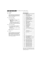
Power Supply Panel: AC Input

(A1) 19

20

SSB: SIM Connector (Male)

(B1) 21

27-29

SSB: IF, I/O Videoprocessing

(B2) 22

27-29

SSB: Feature Box (100Hz Processing)

(B3) 23

27-29

SSB: HOP

(B4) 24

27-29

SSB: Audio Demodulator

(B6) 25

27-29

SSB: Painter

(B7) 26

27-29

SSM: Tuner

(C1) 30

39-44

SSM: I/O’s

(C2) 31

39-44

SSM: Video Buffer

(C3) 32

39-44

SSM: Convergence HV Output1

(C4) 33

39-44

SSM: Convergence HV Output2

(C5) 34

39-44

SSM: Interconnections

(C6) 35

39-44

SSM: Audio Amplifier

(C7) 36

39-44

SSM: Audio Amplifier

(C8) 37

39-44

SSM: Diversity Tables

(C9) 38

39-44

CRT Panel: Red

(DR1) 45

48

CRT Panel: Green

(DG1) 46

48

CRT Panel: Blue

(DB1) 47

48

Large Signal Panel

(E1) 49

54-55

Large Signal Panel

(E2) 50

54-55

Large Signal Panel

(E3) 51

54-55

Mapping Large Signal Panel E1-E3 (Part 1)(E4) 52

54-55

Mapping Large Signal Panel E1-E3 (Part 2)(E5) 53

54-55

Side Jack Panel

(G1) 56

57

ACS Module

(H1) 58

62-63

ACS Module

(H2) 59

62-63

ACS Module

(H3) 60

62-63

Mapping ACS Module H1-H3

(H4) 61

62-63

HOP Panel

(J1) 64

69

HOP Panel

(J2) 65

69

Diversity HOP Panel J1 and J2

(J3) 66

69

Mapping HOP Panel J1 and J2 Part 1

(J4) 67

69

Mapping HOP Panel J1 and J2 Part 2

(J5) 68

69

Keyboard Panel

(K1) 70

71

8.

Alignments

73

9.

Circuit Descriptions, List of Abbreviations, and IC 
Data Sheets

79

List of Abbreviations

96

IC Data Sheets

100

10. Spare Parts List

109

11. Revision List

119

Содержание DPTV565 AA

Страница 1: ...x 100Hz Processing B3 23 27 29 SSB HOP B4 24 27 29 SSB Audio Demodulator B6 25 27 29 SSB Painter B7 26 27 29 SSM Tuner C1 30 39 44 SSM I O s C2 31 39 44 SSM Video Buffer C3 32 39 44 SSM Convergence HV Output1 C4 33 39 44 SSM Convergence HV Output2 C5 34 39 44 SSM Interconnections C6 35 39 44 SSM Audio Amplifier C7 36 39 44 SSM Audio Amplifier C8 37 39 44 SSM Diversity Tables C9 38 39 44 CRT Panel ...

Страница 2: ...ith the On Screen Display menu 1 1 3 Sound Loudspeakers 2 x 4 x6 Full range AutoSound Control Theatre Voice Music Personal Stereo Digital NICAM Sound Output 2 x 12 W_rms 1 1 4 Miscellaneous Ambient Temperature 5 45 C Mains Voltage 160 276 V_ac Mains Frequency 50 60 Hz Power Consumptions Normal Operation 180 W avg Standby 0 7 W Product Dimensions WxDxH cm 43 inch model 106 x 62 x 125 46 inch model ...

Страница 3: ...nel Figure 1 3 Side I O overviews Side I O Cinch Ye Video CVBS 1 0 V_pp 75 ohm jq Wh Audio L 0 5 V_rms 10 kohm jq Rd Audio R 0 5 V_rms 10 kohm jq Side I O 3 5 mm jack Bk Headphone 10 mW 8 620 ohm t Side I O Hosiden SVHS In 1 Y Ground H 2 C Ground H 3 Y 1 0 Vpp 75 ohm j 4 C 0 3 Vpp 75 ohm j 1 3 Chassis Overview Figure 1 4 PWB location G F_15020_028 eps 170305 SSB SSM HOP LSB AC INPUT FOCUS BLOCK FG...

Страница 4: ...he customer touching any internal parts 2 2 Maintenance Instructions We recommend a maintenance inspection carried out by qualified service personnel The interval depends on the usage conditions When a customer uses the set under normal circumstances for example in a living room the recommended interval is three to five years When a customer uses the set in an environment with higher dust grease o...

Страница 5: ...ctrode of the picture tube and the Aquadag coating The semiconductors indicated in the circuit diagram and in the parts lists are interchangeable per position with the semiconductors in the unit irrespective of the type indication on these semiconductors Manufactured under license from Dolby Laboratories Dolby Pro Logic and the double D symbol are trademarks of Dolby Laboratories Figure 2 2 Dolby ...

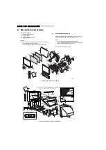
Страница 6: ...0 cabinet AC23 43 CABINET EXPLODED VIEW AC07 AC02 AC01 AC26 AC08 AC03 AC04 Support AC06 chassis frame AC11 AC12 AC20 AC12 AC20 AC11 AC21 AC21 AC22 AC22 AC14 AC15 AC16 AC09 AC33 AC26 AC31 AC22 AC17 mirror AC10 bracket AC27 AC32 AC19 AC28 3135 034 00361 AC31 Module Bracket i Remote DFU Owner s Manual AC34 D D C C C AC13 AC05 B A A A F E G H I E_15000_057 eps 141004 PHILIPS PHILIPS 35 34 2 5 TYPICAL ...

Страница 7: ... Removal 1 Release the metal retainer clips located at the front and rear edges of the SIMM connector 2 Tilt the SSB to the right and then pull it up 4 1 8 Convergence Panel Removal ACS First remove the Module Bracket see the chapter Small Signal Module Removal 1 Carefully pull the ACS panel upward to separate it from the SSM connectors 2 Disconnect the cable assemblies 4 1 9 Wide Band Video Panel...

Страница 8: ...t remove the bolts with pressure springs or the inverted Torx screws of the CRT lens assembly The removal of these components could result in fluid spillage into the PTV cabinet 8 Carefully remove the CRT Lens assembly from the PTV cabinet 4 3 2 Servicing the CRT Lens Assembly Warning Coupling fluid is a poisonous solution containing a high concentration of ethylene glycol Do not leave exposed flu...

Страница 9: ...chamber bladder is visible at the hole of the expansion chamber then replacement of the expansion chamber bladder is required The CRT coupling fluid is critical to the optical performance of the PTV Use only part number 4835 310 67032 3 bottle kit or 4835 310 67031 1 bottle to ensure the optical integrity and performance reliability of the PTV when replacing the CRT coupling fluid 1 Reinstall the ...

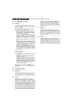
Страница 10: ...olume level set to 25 of the maximum volume level Other picture and sound settings set to 50 mid range The following functions are turned OFF while in SDM Timer Sleep timer The following functions are disabled during SDM and enabled after leaving SDM Parental lock Blue mute Hospitality Mode No ident Timer normally the set is automatically switched off when no video signal IDENT is received for 15 ...

Страница 11: ...of the error buffer are cleared The functionality of the OPTIONS and ALIGNMENTS TUNER WHITE TONE GEOMETRY SOUND and SMART SETTING sub menus are described in the Alignments section chapter 8 How to Exit SAM To exit the Service Alignment Mode press the Power Standby button Note To save the error codes unplug the AC power cord without turning off the set When the power is turned back on the Service A...

Страница 12: ...EL EDIT Select ADD DELETE Set to ADD with the left right cursor keys Line 9 HOTELMODE ON Not Active on AP Units Indicates that the Hotel mode has been activated Line 10 SOURCE Indicates which SOURCE is installed for this preset AV1 AV2 SVHS2 Channel number 8 Line 11 SOUND Indicates which sound mode is installed for this preset Mono Stereo SAP NICAM L1 L2 Virtual or Digital Line 12 VOLUME Value ind...

Страница 13: ...n ComPair can automatically read out the contents of the entire error buffer Diagnosis is done on I2 C UART level ComPair can access the I2 C UART bus of the television ComPair can send and receive I2C UART commands to the micro controller of the television In this way it is possible for ComPair to communicate read and write to devices on the I2C UART busses of the TV set Manually by asking questi...

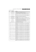
Страница 14: ...ode and not the actual cause e g a fault in the protection detection circuitry can also lead to a protection Table 5 1 Error Code Table Note Error codes 1 2 3 and 4 are protection codes and in this case the supplies of some circuits will be switched off Also in protection the LED will blink the number of times equivalent to the most recent error code Error number Explanation 0 No error 1 FBX 3V3 p...

Страница 15: ...2 This error is caused by corrupted EEPROM data that does not match the data integrity CRC O EEPROM Factory Service 3 Failure This error indicates there was a data integrity failure when accessing the main EEPROM factory service area 3 This error is caused by corrupted EEPROM data that does not match the data integrity CRC P EEPROM Customer Data 1 Failure This error indicates there was a data inte...

Страница 16: ...es would also be given Note If errors 1 2 3 or 4 occur the LED always blinks indicating the last error that occurred even if the set is not in service mode 5 7 Trouble Shooting Tips 5 7 1 Introduction Before the set can be repaired to a component level it is necessary to determine which board is defective The Wiring interconnect diagram is a useful tool for this see chapter 6 5 7 2 Dead Set The St...

Страница 17: ...102 1102 1108 STANDBY POWER SUPPLY 1020 1000 1682 10 9 8 7 6 5 4 3 2 1 3 1 2 4 5 8 6 7 10 9 FBL TXT GND BTXT GTXT RTXT GND RXD GND TXD GND 1 2 3 4 5 6 7 8 9 10 10 9 7 8 6 2 4 5 3 1 FRONT DETECT Y_FRNT_SVHS GND Y_CVBS_FRNT GND C_FRNT_SVHS GND L_FRNT GND R_FRNT 1335 1335 1344 1344 1303 1303 1272 1222 1201 5V_STBY KEYBOARD GND 9V ON OFF LED RC5 1014 1201 7 6 2 5 4 3 1 6 7 5 3 4 1 2 5 3 4 1 2 1349 W W...

Страница 18: ...P34XX AUDIO DECODER 7708 SAA4990H PROZONIC 7714 MSM54V FIELD MEMORY 7715 MSM54V FIELD MEMORY E_15000_002 eps 191004 5V2_CON 3033 5V2_CON SDA S SCL S 3028 3026 SDA NVM SCL NVM WC NVM DATA ADDRESS 84 83 80 97 78 6 5 7 N C N C 3030 5V2_CON 3031 3V3_INTPAINTER 3074 3001 3002 7012 M24C32 NVM EEPROM 7011 CY7C1019 RAM 5P PICNIC 1 2 61 26 15 26 15 62 3746 CLK32 CLK16 89 88 7716 PLCC32 EEPROM 3702 3739 391...

Страница 19: ...VH 7214 BC547B GND_HB I105 I109 GND_HA 5204 F214 10u 5246 2 1 3 I106 7215 IRF9Z24N GND_HC 1 2 7220 BC547B 3 2 1 4 0231 HEATSINK GBU4J 6000 2227 2n2 I131 2214 470u 3011 1 2 3 9004 2 3 5 6 7 8 9 HEATSINK 0218 5202 US28103 1 10 GND_HB GND_HC 4M7 3004 39K 3262 2295 470p GND_HC I004 GND_HC GND_HC 10n 2288 GND_HA 2269 100p 3013 1R0 1 2 3 4 I127 9221 680n 2000 22n 2226 3K9 3249 1110 1 2 1 2 3 4 1R0 3010 ...

Страница 20: ...7 2294 B7 2295 B8 2296 A11 3000 A2 3001 A2 3002 A2 3003 A3 3004 A2 3009 B4 3010 B3 3011 B1 3012 A3 3013 B4 3014 B4 3201 A9 3202 A9 3203 A7 3205 A9 3206 B9 3207 B9 3208 B8 3209 B9 3210 A9 3216 B9 3223 A8 3224 A6 3225 A7 3239 A8 3244 A8 3246 A10 3247 A11 3248 A9 3249 A10 3250 A10 3251 A11 3252 A11 3253 B11 3254 A11 3255 B11 3256 A11 3259 A11 3260 A10 3261 A11 3262 B11 3263 A11 3264 A11 3265 A11 5000...

Страница 21: ...923 G5 4924 G5 4925 F6 4926 G6 4927 F5 4928 F6 4929 F7 4930 G5 4931 G6 4932 G7 4934 G5 4950 F7 B6 95 B6 98 B7 91 B4 64 B4 150 B4 65 F229 B2 62 B4 76 v39 G10 v40 G10 v41 G10 2904 G10 2905 G8 2906 G10 2907 G5 2908 G1 2909 G1 2910 G1 2911 G2 2912 G2 3900 F14 3901 F14 3902 F9 3903 F13 B6 112 F257 4963 4962 4950 4945 4922 v49 v26 v64 3909 220R v35 5902 4912 4954 4903 4902 4965 4919 4949 v71 v43 4958 49...

Страница 22: ...X4 43 54 YCOMBIN 28 YOUT 49 Y_CVBS3 20 Y_CVBS4 23 L8 SVBCOUT 30 SW0 19 SW01 22 SYS1 25 SYS2 27 TUNERAGC 62 UOUT 50 VA 61 VCO1 7 VCO2 8 VIF1 2 VIF2 3 VIFOUT 10 VOUT 51 X3 575 56 HA 60 HPLL 58 IN 12 OUT 13 PIPOUT 32 PLLRILT 6 QSS_AM 5 R1IN 36 R2IN 41 SCL 46 SCOUT 59 SDA 47 SEC_DEC 53 SIF1 63 SIF2 64 COL_PLL 52 COMBOUT 26 CVBS1 16 CVBS2 18 CVBSINT 14 CVBSOUT 34 DEC 35 DIGDEC 33 DIGGND 31 FBL1IN 39 FB...

Страница 23: ... VSSO3 86 VSSO4 111 133 VSSO5 3 VSSO6 VSSX 33 WD RST 7 62 WE A 66 WE B V D 19 V OUT 15 VDDA1 11 VDDA2 22 VDDA3 24 VDDA4 31 64 VDDD1 VDDD2 87 VDDD3 100 135 VDDD4 52 VDDO1 123 VDDO2 148 VDDO3 VIN 26 VSSA1 13 VSSA2 16 129 UVC3 128 UVC4 127 UVC5 126 UVC6 125 UVC7 124 UVC8 91 UVD0 UVD1 92 UVD2 93 UVD3 94 UVD4 95 UVD5 96 UVD6 97 UVD7 98 UVD8 99 V A 29 49 UVA6 50 UVA7 51 UVA8 UVB0 84 UVB1 83 UVB2 82 UVB3...

Страница 24: ...TC144EU 10p 2304 33K 3453 7309 1K8 3358 4K7 3365 2334 2u2 V29 V25 V24 V27 V26 BAT254 6307 6314 MCL4148 FOR PTV SET RES ONLY FOR NO HOP GND RGB CRT 4308 4309 2341 100u 10p 2308 5302 6u8 100u 2300 3391 68K BC857BW 7303 4K7 V20 3394 6u8 5301 10K 3467 PDTC144EU 7304 100R 3387 2310 10p 2343 100n 100K 3359 4302 2u2 2333 100K 3323 100K 3301 33K 3465 BC847BW 7305 BC847BW 7306 5307 100MHZ BC847BW 7311 3308...

Страница 25: ...S 7656 B 5 3 4 RES 7656 A 7664 A BC847BPN 2 6 1 RES 3545 7664 B BC847BPN 5 3 4 3698 1K2 3658 150K 3637 100K 3657 47K 150K 3666 100K 3667 1K2 3671 3695 3654 6K8 22K 330n 2661 1K 3532 3688 6K8 3699 RES 3690 22K RES 3639 C100 2693 220p 6K8 3686 22K 330n 2502 3684 22K 3687 3689 6K8 2503 330n 1n 2674 330n 2505 4688 A 2644 1n 2694 330n 2643 1n 2668 3p3 3613 RES 2678 10u 6652 BZX284 C10 RES 3634 4632 A R...

Страница 26: ...NTD_ 61 IREF 35 MVX RD 74 MVX WR 68 OSCGND 69 P0 0 TX 16 P0 1 RX 17 P0 2 INT2 18 P0 3 INT3 22 P0 4 INT4 24 P0 5 13 P0 6 28 P0 7 T2 29 P1 0 INT1 76 66 AD0 85 AD1 86 AD2 87 AD3 88 AD4 89 AD5 90 AD6 91 AD7 92 ALE 20 B 46 CORB 43 CVBS0 31 CVBS1 32 EA_ 14 FRAME 41 G A11 64 A12 37 A13 36 A14 8 A15 BK 33 A15 LN 7 77 A16 LN A17 LN 3 A2 39 A3 38 A4 27 A5 26 A6 23 A7 15 A8 67 A9 7001 SAA5667HL A0 49 A1 40 A...

Страница 27: ...Circuit Diagrams and PWB Layouts 27 DPTV565 AA 7 Layout SSB Top Side E_15000_133 eps 191004 8204 000 6507 3 ...

Страница 28: ...B3 2312 B3 2313 B3 2319 B3 2320 B3 2321 B3 2323 B3 2325 B3 2326 C3 2328 B2 2342 C2 2343 C2 2354 C3 2366 C4 2369 C3 2370 C2 2371 B3 2372 B3 2374 C3 2375 C3 2378 B4 2384 C4 2385 C3 2386 C2 2390 C4 2392 C3 2399 C4 2402 C4 2418 B3 2419 B3 2420 C3 2421 C3 2422 C4 2423 C3 2424 C3 2426 A4 2431 B3 2501 B1 2502 B1 2503 B1 2504 B1 2505 B1 2506 B1 2507 B1 2509 C1 2510 C1 2511 C1 2512 C1 2513 C1 2550 B1 2551 ...

Страница 29: ...Circuit Diagrams and PWB Layouts 29 DPTV565 AA 7 Layout SSB Bottom Side E_15000_134 eps 191004 8204 000 6507 3 ...

Страница 30: ...2083 15K 3000 F101 I110 I109 I182 6 F3 6 F7 6 F3 47R 3114 47R 3115 0 106451 1 1002 1 2 6 J3 1u0 2013 8 D7 F104 I170 6 H6 6 A11 1 F12 47n 2085 10u 2114 2u2 2116 50V 1 2 F111 B2B PH K 1301 I148 25V 100u 2078 6 E11 I107 I105 F109 F112 F102 I101 3015 15K 8 9 F106 B10B EH A 1 10 2 3 4 5 6 7 6011 BAS216 I171 6 F7 5007 5u6 NOTES 2 F108 1302 B2B PH K 1 0 106451 1 1003 1 2 F128 TU 7 V SUPPLY V SUPPLY 14 MT...

Страница 31: ... 47K 3002 1R0 3142 100R 3058 6 F3 BC847B 7016 9012 9011 100R 3053 F226 6 D6 2069 22p 100R 3047 F229 F228 F249 F247 8 F251 1024 B YKC21 8024 5 6 7 F225 2830 1n0 F217 F216 F210 F208 F211 F209 L SC2_AV2 IN 9V Vp Vp F203 9V L CL_VL OUT CVBS SC2_MON OUT R CL_VL OUT Vp Y R SC2_AV2 IN Vp CVBS SC1_AV1 IN L SC1_AV1 IN R SC1_AV1 IN Pb Pr 3012 242202512479 934038640115 BZX284 C6V8 BZX284 C6V8 NOT USED 3007 2...

Страница 32: ...842 2807 2u2 39K 3813 I308 I336 I335 6 D4 I328 6801 BZX384 C9V1 1K0 3828 2814 100n 3852 68K I338 8 G8 6 C7 470R 3816 I313 8 H12 3838 330R BC857B 7809 3853 68K 6 D7 F303 I334 I319 2813 470u 25V I305 10R 3809 1K0 3804 270R 3815 6 E4 3314 10R 3321 10R 3832 68K 680R 3846 3322 10R 8 F8 3857 680R 1K0 3807 3835 680R 150R 3805 2u2 2803 3836 100R BC847B 7800 I315 6 C4 2u2 2801 I330 2 I5 I302 F301 100K 3812...

Страница 33: ...C 4K7 3167 GND C 150p 2100 GND C F422 GND C 6R8 3149 GND C F405 F420 1 2 3 4 F406 GND C B4P VH 1007 F423 GND C I429 5 D12 I400 5 B1 6 G11 5 I12 4 I5 22K 3033 I421 5 G12 150p 2111 100R 3165 GND C GND C 100R 3162 6R8 3152 GND C F427 I401 GND C 100u 2037 3K3 3098 F403 5 F4 F418 GND C GND C 6 C11 F409 I435 100R 3164 6R8 3150 I408 2064 6R8 3158 F424 150p 2065 150p GND C GND C 100R 3166 3K3 3090 150p 21...

Страница 34: ...R 3197 PMBT2369 7018 6 G11 4 B1 4 I5 470u 2059 6007 BYD33D BAS216 6041 2044 330p 2055 1n0 BAS216 6047 100n 2161 4K7 3168 3K3 3074 4 E13 7004 BC847B BAS216 6051 100K 3031 GND C 2K7 3190 GND C 3038 100R 10R 3082 9040 100K 3020 9041 100R 3063 I518 4 A13 BF550 7006 2 1 3 IRF9Z24N 7020 6044 BZX284 C6V8 BAS216 6048 100u 2153 470u 2058 GND C 3200 470R 3136 8K2 I521 3K3 3067 I515 1n0 2156 10R 3193 I510 90...

Страница 35: ...613 I640 F628 F619 3018 1K0 8 F8 5008 2 D8 HEATSINK 0102 5009 15u 4008 2006 100n 3182 10K 2005 100n IN OUT 5 I12 4 B1 4 I5 7102 L7908CV GND 4006 F608 TPSRD 1200 2 1 I 3 O F610 4M5 F626 F607 1 D3 330R 3039 78 8 80 10 12 14 16 18 81 82 6 60 62 64 66 68 70 72 74 76 40 42 44 46 48 50 52 54 56 58 22 24 26 28 30 32 34 36 38 4 87613 8011 ROW_B 1020 B 2 20 9016 3 D12 3017 330R I620 GND C 1K0 S1D 6005 3071...

Страница 36: ...7 2712 A7 2713 B8 6 H11 18V D E 1349 A9 1700 A8 1701 C8 2117 C7 2701 A3 2702 B5 1 INV1 8 INV12 9 INV2 2 MUTE 4 I707 TDA2616Q 7700 68K 3780 2706 220n 3722 10R 2715 22n 2713 22n 3792 1K0 100n 2705 2735 100u 3798 BZX284 C6V8 2m2 2730 2117 2m2 47K 3799 1 2 3 5 1349 26 62 6051 F706 F704 F705 7705 BC847B 3720 47K 2714 47n 47n 2716 I709 I708 1701 2A T I959 1700 2A T 3781 680K BC847B 7704 2701 2703 2711 1...

Страница 37: ...V 9006 GND C 9005 2816 100n 1u0 2106 9038 INA_NEG 2 INA_POS 3 INB_NEG 6 INB_POS 5 OUTA 1 OUTB 7 VDD 8 4 VSS TDA1308 7403 3420 10K 6052 BAS316 I821 3412 33K 430R 3139 50V 1 G8 2412 100u 3140 1R0 1 9039 1604 SIN 21T 1 8S B 16V 220u 2802 SIN 21T 1 8S B 1608 1 1607 SIN 21T 1 8S B 1 2411 470n F611 3440 100K F816 I814 I819 47u 2110 F813 9048 3442 1K0 1 GND C 1600 SIN 21T 1 8S B 3422 10K I806 3447 100K F...

Страница 38: ...OT USED 319802151010 100R NOT USED NOT USED NOT USED NOT USED NOT USED NOT USED 1303 NOT USED 319802151020 9019 1K0 319803690010 NOT USED NOT USED NOT USED 3443 SIN 21T 1 8S B NOT USED 319803690010 NOT USED NOT USED NOT USED NOT USED 242202516049 09JL BT E 100K BZX284 C6V8 NOT USED NOT USED NOT USED Ref Des 3135_037_11351_01 47R NOT USED NOT USED 330R NOT USED NOT USED NOT USED NOT USED 50V 319803...

Страница 39: ...7021 C9 7022 F8 7044 E7 7045 E10 7101 F3 7102 F2 7103 F4 7104 A8 7105 A3 7106 F6 7700 A10 9003 C4 9004 C4 9005 C4 9006 C4 9007 A5 9008 C4 9009 B8 9010 B8 9011 B2 9012 C2 9013 C2 9016 A5 9017 A5 9018 B5 9019 B5 9022 A8 9023 A8 9030 D4 9031 D4 9032 D4 9033 D4 9037 E5 9038 E5 9039 C5 9040 D9 9041 E10 9042 C9 9044 E6 9045 E7 9046 B9 9047 C7 9048 D5 9049 E5 9050 D5 9105 A2 9106 A3 9107 B2 9108 A6 9109 ...

Страница 40: ...9 E3 3103 A11 3106 B11 3107 B11 3108 B11 3109 A11 3110 D5 3111 B7 3112 D5 3114 A11 3115 A11 3132 D5 3133 D5 3134 D5 3138 F7 3139 F7 3146 B11 3147 E2 3148 E3 3167 E4 3168 D5 3169 E2 3170 D6 3182 B8 3190 B3 3191 B4 3193 C3 3194 B3 3195 C4 3196 B4 3197 B4 3199 C4 3200 C4 3201 D3 3202 F3 3304 E7 3305 D6 3313 D7 3314 D6 3321 D7 3329 E7 3412 B5 3415 B5 3416 B5 3419 A4 3420 A4 3423 A5 3440 E11 3441 E11 3...

Страница 41: ...Circuit Diagrams and PWB Layouts 41 DPTV565 AA 7 Layout SSM Part 1 Bottom Side F_15020_011a eps 110305 Part 1 ...

Страница 42: ...42 DPTV565 AA 7 Circuit Diagrams and PWB Layouts Layout SSM Part 2 Bottom Side Part 2 F_15020_011b eps 110305 ...

Страница 43: ...Circuit Diagrams and PWB Layouts 43 DPTV565 AA 7 Layout SSM Part 3 Bottom Side F_15020_011c eps 110305 Part 3 ...

Страница 44: ...44 DPTV565 AA 7 Circuit Diagrams and PWB Layouts Layout SSM Part 4 Bottom Side F_15020_011d eps 110305 Part 4 ...

Страница 45: ...D7 I123 D2 I125 D7 I127 D7 I128 E7 I133 F1 I134 F3 I135 G3 1K5 22R N U 1K5 68K 330R 0V5 4V 3V3 8V1 4V 2K2 N U 3203 6K8 3228 1K5 TO HOP 0V1 3230 3229 3213 680R 1 2 75R 3200 1201 B2P VH F105 100p 2218 5201 F125 4001 9 10K 3210 1 10 11 12 4 5 6 7 8 HPS0521 01 4906 1203 2201 100n I112 I128 220R 3218 1208 RT 01T 1 0B 3209 6200 BYD33M I111 3217 1R0 1 2 3 4 5 1K5 3202 1207 S5B EH NOTES I123 RTB 1 5 1F 12...

Страница 46: ... 8V1 4V 2K2 N U RTB 1 5 1F 1204 I123 3203 6K8 3228 1K5 TO HOP 0V1 3230 3229 3213 680R 1 2 75R 3200 1201 B2P VH F105 100p 2218 5201 F125 4001 9 10K 3210 1 10 11 12 4 5 6 7 8 HPS0521 01 4906 1203 2201 100n I112 I128 220R 3218 1208 RT 01T 1 0B 3209 6200 BYD33M I111 3217 1R0 1 2 3 4 5 1K5 3202 1207 S5B EH 6205 BZM55 C3V9 3231 1K5 3232 5200 1 2 3 7202 BF570 1211 TMPJ02X A1 F104 I104 2215 1u0 6201 BAS21...

Страница 47: ...1 4V 2K2 N U RTB 1 5 1F 1204 I123 3203 6K8 3228 1K5 TO HOP 0V1 3230 3229 3213 680R 1 2 75R 3200 1201 B2P VH F105 100p 2218 5201 F125 4001 9 10K 3210 1 10 11 12 4 5 6 7 8 HPS0521 01 4906 1203 2201 100n I112 I128 220R 3218 1208 RT 01T 1 0B 3209 6200 BYD33M I111 3217 1R0 1 2 3 4 5 1K5 3202 1207 S5B EH 6205 BZM55 C3V9 3231 1K5 3232 5200 1 2 3 7202 BF570 1211 TMPJ02X A1 F104 I104 2215 1u0 6201 BAS21 DS...

Страница 48: ... C2 3210 B1 3212 A1 3217 B2 3218 B1 3226 A2 3233 A1 5200 B2 5201 B2 6200 C2 7201 A2 9200 C1 Layout CRT Panel Bottom Side 3141 083 3002 1 F_15020_017 eps 170305 2200 B2 2201 A2 2204 A2 2207 A2 2209 A2 2212 B2 2213 A2 2214 B2 2215 B2 2219 A2 2220 A2 2221 B2 2224 B2 3200 A2 3201 A2 3203 A2 3204 A2 3206 B1 3208 A2 3209 A2 3211 B1 3213 A2 3214 B2 3216 B2 3223 A2 3225 A2 3227 A2 3228 A2 3229 A2 3230 A2 ...

Страница 49: ... 2311 3 1 4 6 GND_C W8051 5330 3382 100K F131 3362 6K8 F125 2n2 2301 11 12 2 3 4 5 6 7 8 9 B12B EH A 1518 1 10 2305 470p 4K7 3356 47K 3350 F132 GND_C 2334 4n7 3385 1K0 3309 0R22 2 C20 5315 2365 1m0 5304 2354 47u 25V F141 680p 2310 68K 3359 F139 GND_C 2312 470p I172 3390 1K0 2382 100p 330p 2304 4K7 3352 I189 2 N19 NOTES GND_C I130 I165 5312 3303 I144 100K 10u 5336 I170 I173 470p 2329 I171 1N4148 63...

Страница 50: ... 7808 I867 1804 MRT T 1A 2803 470p I844 6829 BAS216 BC847B 7813 2845 100n I811 3 E3 1 N20 BAS216 6823 I852 3 J1 2814 470p 3K3 3840 4 7 5813 120u 5812 1 7807 BSN304 3842 10K BC847B 7809 3857 10K 3848 33K 3843 2K2 3855 330R BAS216 6807 1K0 3827 2 L10 100n 2806 3860 47K I880 I866 6804 BZX79 C4V7 3 D3 I825 1R0 3817 I875 I857 2 K1 1K0 3825 22K 3845 F808 2838 1n0 3 F3 I873 2839 1n0 I835 I868 I840 150p 2...

Страница 51: ...3 4K7 3934 BYV27 400 6917 2914 10u 2906 1n0 3915 2K2 I917 2902 2n2 BC847B 7902 2907 4n7 I920 I954 I919 BAT254 6919 I957 I923 7903 BC327 25 3910 6K8 F933 F936 4u7 2920 I941 3921 470K 10K 3922 F939 4 8 6 100n 2916 W8073 5901 1 3 3935 2M2 1901 B3B EH A 1 2 F904 I915 3929 10K 3930 100R 3911 56K 3906 1K0 6 7 8 9 I935 1 10 11 12 2 3 4 5 14 1510 B12B EH A 5904 HVG 4 F900 1504 B3P LV TA 1 2 3 3918 680R 2 ...

Страница 52: ...ms and PWB Layouts Mapping Large Signal Panel E1 E3 Part 1 5 4 3 2 1 J I H G F E D C B H G F E D C B A 1 7 6 5 4 3 2 13 12 11 10 9 8 13 12 11 10 9 8 7 6 J I A KDR2K4 LARGE SIGNAL PANEL AP E4 E4 E_15000_028 eps 131004 3135 033 3425 3 ...

Страница 53: ...uts 53 DPTV565 AA 7 Mapping Large Signal Panel E1 E3 Part 2 H G F A 5 4 3 2 1 J I I E D C B A H G F E D C B 1 5 4 3 2 J HDR2K4 LARGE SIGNAL PANEL AP E5 E5 E_15000_029 eps 191004 3135 033 3425 3 Personal Notes E_06532_012 eps 131004 ...

Страница 54: ...09 E9 3811 G10 3812 G10 3815 G8 3817 C7 3818 F9 3819 F7 3820 F8 3821 F8 3822 E11 3828 F7 3829 F11 3834 G11 3837 F11 3838 F9 3839 F10 3840 F10 3844 F11 3846 D8 3850 D10 3859 B11 3860 C11 3862 B11 3864 A11 3866 F11 3871 E10 3880 D11 3900 E11 3901 A8 3902 A8 3904 E11 3905 F11 3907 A10 3908 A11 3909 A10 3910 F11 3911 F11 3912 D11 3913 F11 3914 F11 3915 F11 3916 F9 3925 G11 3926 G10 3927 B11 3931 G10 3...

Страница 55: ...F6 3384 F6 3385 F6 3813 F3 3814 G3 3823 F1 3825 E2 3826 E1 3827 F1 3833 E2 3835 F1 3836 F1 3841 D1 3842 D1 3843 D1 3845 D1 3847 C3 3848 C2 3849 D2 3851 C1 3852 C1 3853 C2 3854 C2 3855 C2 3856 C2 3857 C2 3858 C2 3861 D3 3865 G4 3867 D1 3868 D1 3870 E2 3903 C3 3906 C2 3917 D2 3918 D2 3919 D2 3920 C1 3921 E1 3922 E1 3923 G1 3924 G1 3928 G2 3929 G2 3930 G2 3932 F2 4101 C2 4103 D1 6807 E4 6808 E4 6813 ...

Страница 56: ... 2 K NOT USED 6004 934038640115 BZX284 C6V8 934038640115 BZX284 C6V8 934038640115 BZX284 C6V8 BZX284 C6V8 934038640115 BZX284 C6V8 934038640115 BZX284 C6V8 NOT USED 934038640115 BZX284 C6V8 NOT USED NOT USED 6011 BZX284 C6V8 NOT USED NOT USED D T V R D X M N E _ 3 K 3135_037_11961 X X 3135_037_12131 223891019854 X 9 2 H T O S U _ 934038640115 BZX284 C6V8 NOT USED 934038640115 BZX284 C6V8 NOT USED ...

Страница 57: ... A1 Layout Side Jack Panel Bottom Side F_15020_020 eps 100305 3141 083 3008 1 2000 A1 2001 B1 2002 B1 2005 B1 2006 B1 2008 C1 2009 C1 3000 B1 3001 A1 3002 B1 3005 B1 3006 B1 3007 B1 3009 B1 3019 C1 3020 C1 3023 C1 3026 C1 3027 C1 3028 C1 3029 C1 3030 A1 4000 A1 4001 A1 4002 C1 6000 A1 6001 A1 6002 A1 6003 A1 6004 A1 6005 B1 6006 B1 6007 B1 6008 B1 6009 B1 6010 B1 6011 C1 6012 C1 6013 C1 ...

Страница 58: ...6 TBU5 35 TBU6 34 TBU7 33 TEST 11 VBLK 10 VCCA 50 VCCB 62 VCCC 70 58 OPTI 72 OPTT 74 OSCL 21 PORA 80 PORB 79 PORC 78 POUT 77 REFC 55 REFN 54 REST 13 SCLM 2 SCLS 9 SDAI 8 SDAM 1 SDAO GNDD 20 GNDF 23 GNDG 43 GNDH 41 53 GNDI GNDJ 29 GNDK 4 GNDL 30 GNDM 76 GNDN 15 GNDP 56 GNDQ 3 GRES 22 MLIN 75 OGAH 57 OGAV 66 DNBH 45 DNBV 60 DNGH 48 DNGV 63 DNRH 51 DNRV 65 ECLK 14 FILT 24 FLT2 25 FOCR 68 FOCS 69 GNDA...

Страница 59: ... P1 0 INT1 76 P1 1 T0 78 P1 2 INT0 79 P1 3 T1 80 P1 4 SCL1 83 P1 5 SDA1 84 P1 6 SCL0 81 90 AD6 91 AD7 92 ALE 20 B 46 CORB 43 CVBS0 31 CVBS1 32 EA_ 14 FRAME 41 G 47 HSYNC 53 INTD_ 61 IREF 35 MVX RD 74 MVX WR 68 OSCGND 77 A16 LN A17 LN 3 A2 39 A3 38 A4 27 A5 26 A6 23 A7 15 A8 67 A9 66 AD0 85 AD1 86 AD2 87 AD3 88 AD4 89 AD5 7100 SAA5667HL A0 49 A1 40 A10 65 A11 64 A12 37 A13 36 A14 8 A15 BK 33 A15 LN...

Страница 60: ... 3348 100R 1 E2 BAS216 6308 3201 100R 100R 3325 4302 2 L15 F301 9V F024 100R 3350 1 N8 100R 3200 2312 100n 10p 2319 100R 3309 4303 10p 2317 2 I15 BAS216 6309 5V 2 K3 1 N8 2 M3 1 G2 5V 2 D18 7015 BC847B 1K0 3326 1 N15 10K 3332 1 N14 1 I2 47R 3317 4305 2 M15 2 M15 F028 3314 47R 4301 5V 2 H15 4304 1 E2 1 F2 NC 6 PFI 4 PFO_ 5 RESET 8 RESET_ 7 VDD 2 2 H15 1 D2 2 K3 7301 TPS3707 33D GND 3 MR_ 1 100R 330...

Страница 61: ...Layouts 61 DPTV565 AA 7 Mapping ACS Module H1 H3 12 11 10 9 13 8 13 12 11 10 9 8 7 6 5 4 3 2 1 J I H G E D C B A F I H G F E D C B A J 1 7 6 5 4 3 2 AUTO CONVERGENCE AUTO CONVERGENCE H4 H4 E_15000_039 eps 111004 3135 013 3233 3 ...

Страница 62: ...4 2050 B4 2051 B4 2052 B4 2053 B4 2054 B4 2055 B3 2056 B4 2057 C4 2058 B4 2059 B4 2200 A4 2201 A4 2206 A3 2207 A3 2210 A3 2211 A2 2235 A3 2251 A4 2252 A4 2279 A1 2280 A1 2281 A1 2282 A1 2310 C4 2312 B4 2313 B4 2314 B4 2315 C4 3021 B2 3034 B3 3045 B2 3048 B3 3049 B3 3053 C3 3054 C3 3063 B3 3064 B3 3068 B3 3069 B3 3070 B3 3073 B3 3074 B3 3075 B3 3084 B4 3090 C4 3091 C4 3092 C4 3218 A3 3219 A3 3235 A...

Страница 63: ... C3 3085 B2 3086 B1 3087 B2 3088 B1 3089 B2 3200 A1 3201 A1 3202 B2 3203 B3 3204 B2 3205 B2 3206 B2 3207 B2 3208 B2 3209 B2 3210 A1 3211 A1 3212 B3 3213 A2 3214 B3 3215 A3 3216 B2 3217 B2 3220 B2 3221 B2 3222 B2 3223 A3 3224 A3 3225 A3 3226 A3 3227 A3 3228 A2 3229 A2 3230 A2 3231 A2 3232 A2 3233 B3 3234 A1 3240 A1 3241 A3 3242 A3 3243 A3 3282 A3 3291 A3 3292 A3 3293 A4 3298 A1 3299 A1 3306 C2 3307...

Страница 64: ...1K0 3447 390R 3713 1K0 3471 1K0 2602 1n0 2802 1u0 EH B 1700 1 2 3 100n 2952 2627 100n 3 2 1 8 4 NOTES 7900 1 LM393D 39K 3715 1n0 2490 100n 2809 1K2 3730 F810 F809 1K0 3723 180R 3432 F905 1K0 3470 390R 3464 F963 100K 3496 100R 3454 47R 3638 3637 47R 100n 2968 3951 1R0 1u0 2923 1n0 2913 3646 100R 3624 100R 2482 1n0 3635 47R 100R 3614 100n 3424 390R 1 2 3 2416 EH B 1710 2 K1 2u7 5411 1u0 2901 22R 343...

Страница 65: ...2R 3807 4K7 47u 2150 BAS316 6172 2329 100n 22R 3521 4230 47R 3131 F250 2520 47u BAS316 6141 470p 2322 3250 75R 1 C19 F260 6132 BAS316 47u 2120 3150 75R 470R 3517 3336 100R 3280 1K0 F222 1n0 2505 2502 100n BAS316 6122 BAS316 6171 8 100n 2507 7328 A 74HC4538D 1 3 4 5 7 6 2 16 22R 3505 1 F20 F214 2290 47u F115 2191 100n 7530 BF570 F113 2326 68p 1K0 3180 3185 1K0 3519 3K9 3530 330R 47u 2230 3513 1K8 F...

Страница 66: ...6 NOT USED NOT USED 6121 319801010630 BAS316 NOT USED NOT USED 6331 NOT USED NOT USED 319801010630 BAS316 NOT USED NOT USED 6131 4220 NOT USED 319802190020 NOT USED 4221 NOT USED 319802190020 NOT USED 4223 NOT USED NOT USED NOT USED 6141 319801010630 BAS316 NOT USED NOT USED 6142 319801010630 BAS316 319802151010 100R 3335 NOT USED NOT USED 319802151010 100R 3336 NOT USED 319801010630 BAS316 NOT US...

Страница 67: ...Layouts 67 DPTV565 AA 7 Mapping HOP Panel J1 and J2 Part 1 HDR2K4 HOP 28KHZ AP AUG 1 7 6 5 4 3 2 13 12 11 10 9 8 13 12 11 10 9 8 7 6 J I D C B A H G F E D C B A 5 4 3 2 1 J I H G F E J4 J4 3135 033 3429 2 E_15000_045 eps 111004 ...

Страница 68: ...t Diagrams and PWB Layouts Mapping HOP Panel J1 and J2 Part 2 J I HDR2K4 HOP 28KHZ AP AUG H G F E D C B A 1 4 3 2 4 3 2 1 J I H G F E D C B A J5 J5 3135 033 3429 2 E_15000_046 eps 191004 Personal Notes E_06532_012 eps 131004 ...

Страница 69: ...3430 B3 3431 A3 3432 A3 3433 A3 3434 A3 3435 A3 3436 B3 3438 A3 3439 A2 3441 B2 3442 B2 3443 B2 3444 A2 3445 B2 3446 A2 3447 A2 3448 B2 3449 A2 3450 B3 3451 B3 3452 B3 3453 B3 3454 B3 3455 B3 3456 B3 3458 B3 3459 B2 3460 B2 3461 B3 3462 B2 3463 B2 3464 B2 3465 B2 3466 B2 3467 B2 3468 B2 3470 A3 3471 A2 3480 B3 3481 B2 3490 B3 3491 B2 3495 A3 3496 A2 3500 C3 3501 C2 3502 C3 3505 C2 3506 B2 3507 C2 ...

Страница 70: ...D5 I013 B6 I014 B7 I015 B8 I016 B8 I017 B8 I018 B9 I019 B9 I020 A6 I021 B3 I022 B3 I024 B4 4120 3108 6K8 3113 4K7 I007 5 6 7 8 4 NOTES LM358DR2 7000 2 1405 SKQNAB 1407 SKQNAB 1403 SKQNAB 1406 SKQNAB I002 1402 SKQNAB I001 6104 BPW46 1 GND GND 3 OUT OUT 2 VS VS TSOP1736UU1 6105 2104 470n 1M5 I024 3115 1 3 3104 1K5 TLDR5400 6110 1 2 3107 330R TLUV5300 ORANGE RED 6101 1 3121 560R 3111 10K I021 3118 3K...

Страница 71: ...3 eps 100305 3135 033 3343 5 1201 1202 1301 1401 1402 1403 1404 1405 1406 1407 2101 2103 3109 6101 6104 6105 6110 9102 2102 3107 3108 4101 F_15020_024 eps 100305 3135 033 3343 5 2102 2104 3100 3101 3102 3103 3104 3105 3106 3107 3108 3110 3111 3112 3113 3114 3115 3116 3117 3118 3121 3122 4100 4101 4120 4121 6102 6103 7000 ...

Страница 72: ...72 DPTV565 AA 7 Circuit Diagrams and PWB Layouts Personal Notes E_06532_013 eps 131004 ...

Страница 73: ...iewing screen 3 Adjust the CRTs focus control located on the Screen Focus Control Block for the sharpest raster image 4 Confirm correct focus by viewing the screen from the front of the set 5 Repeat steps two through four to adjust the focus of the two remaining CRTs Note Before beginning the following adjustment procedures set the customer picture sharpness brightness and tint controls to midrang...

Страница 74: ...black and white part of the test pattern are at the same position Default value is 9 LUM DELAY PAL I Apply a PAL I colour bar grey scale pattern as a test signal Adjust this parameter until the transients of the colour part and black and white part of the test pattern are at the same position Default value is 9 LUM DELAY SECAM Apply a SECAM colour bar grey scale pattern as a test signal Adjust thi...

Страница 75: ...able the Convergence drive Select GEOMETRY in the menu and enter the following default values for the mode being adjusted Table 8 3 Geometry Default Values After entering the default values the E W WIDTH VERTICAL SLOPE and VERTICAL AMP should be the only settings requiring further adjustment Note Perform and store Convergence alignment after any changes to the Geometry 8 4 4 Convergence Mode There...

Страница 76: ... 2 Convergence alignment grid 8 4 6 Single Tube Replacement Convergence If a single tube has been replaced it is not necessary to do a Major Convergence alignment 1 Enter the Convergence mode and select the adjustment needed 2 Select Red to Green for example if the Red tube has been replaced 3 Adjust the centring rings on the CRT to centre the Red pattern onto the Green pattern 4 Starting with the...

Страница 77: ...N in the selection menu Using the same method that was used to adjust the Green Grid to the Template adjust the Red Grid onto the Green Grid If the set is a later production select SP RED to centre the Red grid onto the Green grid Exit this mode by pressing the MENU button Then select the MP RED to adjust the Red onto the Green using the 35 point adjustment When this is complete select the RED TO ...

Страница 78: ...O in the SERVICE OPTIONS level Locate the option code label on the inside right panel of the unit and enter the correct codes for the model being serviced Example Group 1 49483 32801 33055 32793 Group 2 39897 32768 32768 00000 Note Remember to cursor to the STORE OPTIONS level and select OK to save these changes Menu name Subjects Option s Physically in set Personal Options Picture Mute Yes Pictur...

Страница 79: ...B Small Signal Board This is a multi system sound decoding processor The audio amplifier is located on the SSM Small Signal Module This is a 24 Watt 2 x 12 Watts digital amplifier There is also a Headphone output located on the Side Jack Panel The headphone amplifier is located on the SSM Sound system 30 W 2x15W Audio Headphone Out Speaker on Off 9 2 Power Supplies The Rectifiers and Standby Suppl...

Страница 80: ... to the set in the Standby mode When the set is turned on it provides the 15 9 and 5 2 Volts supplies Standby B is applied to the Standby Switching regulator 7218 via pins 5 and 3 of 5202 An internal switch in 7218 charges capacitor 2283 connected to pin 1 of the IC When the charge on 2283 reaches 5 8 Volts the internal switch switches to internal The IC is now being powered by the charge on capac...

Страница 81: ...a resistors 3262 and 3263 This will cause the 15UV line to go high In the Standby mode the Standby line is high turning transistor 7222 on When the set is turned on 7222 turns off Capacitor 2296 provides a delay to prevent the 15UV line from going high before the 15V supply turns on This circuit can be defeated by grounding the base of transistor 7220 When repairs are complete this jumper should b...

Страница 82: ...oved from the set while it is turned on The voltage from pin 18 is rectified by 6318 and is applied to the Shunt Regulator 7305 Shunt Regulator 7305 is turned on keeping the Power Fail and Protect lines Low When AC is removed while the set is on 7305 will turn off fast This is because the filter capacitor for the input to 7305 is small When 7305 turns off the Power Fail line goes high from the vol...

Страница 83: ...is a connector in the SVHS input the composite input is muted Resistors 3001 3002 and 3000 on the Video Y and C lines provide 75 ohm impedance matching If a cable is plugged into the SVHS connector the line connecting resistor 3029 to ground is removed causing the voltage on the Y C_CVBS_SENSE_FRNT line to increase This signals the microprocessor to switch the video switching circuits from composi...

Страница 84: ...output on pin 60 and 61 pin 60 is the Line sync while pin 61 is the Frame sync Line sync is also output on pin 59 to synchronize the Three Line Comb filter When the Component input is selected by the YUV switch a DVD player for example the Y signal is selected by 7017 on the SSM and fed to pin 20 of 7323 The selected Y signal is then fed to the internal Sync Separator 9 3 5 SAW Filter Switching Fi...

Страница 85: ...his is an impedance matching and YPbPr to YUV circuit This circuit does not invert the signal The Pb signal is amplified by 7802 and buffered by 7803 The Pr signal is amplified by 7804 and buffered by 7805 The Pb and Pr signals are inverted 9 3 9 Feature Box Figure 9 16 FBX block diagram E_15000_079 eps 181004 E_15000_080 eps 181004 CLAMP AGC PREFILTER AGC CLAMP PREFILTER AGC CLAMP PREFILTER TIME ...

Страница 86: ...sync is output on Pins 18 and 19 9 3 10 Eagle Figure 9 17 Eagle The Eagle circuit provides Skin tone correction Blue stretch and Green Enhancement In versions equipped with the Pixel Plus feature the Eagle IC performs the corrections for this mode The video frames are sent to FM4 and FM5 7722 and 7723 memories from the FALCONIC IC These memory ICs hold the frame data until they are required for pr...

Страница 87: ... the maximum drive voltage for the cathode Once the Calibration has taken place the Output Amplifiers switches to the RGB drive signal as the output Horizontal and Vertical Sync is fed to 7600 on Pins 23 and 24 IC 7600 processes the sync to provide the geometry for the picture Horizontal drive is output to the sweep circuit on pin 8 Vertical drive is output on Pins 1 and 2 East West drive is outpu...

Страница 88: ...d Red CRTs the inverting input on pin 2 will become greater than the non inverting input on pin 3 resulting in the output on pin 1 to go Low The ABL line will go Low causing 7600 to reduce the drive to all of the CRTs This circuit prevents the Blue tube from being over driven 9 3 17 HOP Analogue Control Figure 9 24 IC7800 HOP analogue control IC 7800 develops the analogue control voltage for the H...

Страница 89: ...l is fed to 7807 on the Large Signal panel Transistor 7807 drives the Horizontal Output Transistor 7801 which drives the Yokes and the Horizontal Output Transformer 5801 Transformer 5801 produces plus and minus 13 Volt supplies for the Vertical Output circuit It also produces a 200 Volt source and Filament voltage for the CRT panels The output of 7807 also drives 7803 and 7802 which drives the Dyn...

Страница 90: ...namic Focus drive The DAG line along with the output on pin 2 is connected to 7903 to produce the ABL voltage for the set If an over current condition should develop with the drive the ABL voltage will go Low turning 7905 on latching 7904 which will remove drive to pin 8 of the HVG This will cause the High voltage to shut off Vertical Parabola drive is fed to 7901 to produce the Vertical component...

Страница 91: ...hat mode must be applied to the set during the convergence alignment The output of the DACS is fed to six op amps before being fed to the Power Amplifiers located on the SSM When screen centring is being performed it is necessary to disable the convergence drive waveform A High on pin 77 turns transistor 7029 on turning 7038 on which turns transistors 7032 7033 7030 7031 7034 and 7035 on This mute...

Страница 92: ...ternally decoded audio from selected audio IF on the SSB The Processor outputs line level Left and Right monitor audio and line level Sub Woofer out These jacks are located on the SSM It also outputs Left and Right audio to the Audio Amplifier located on the SSM Left and Right audio is output to a Headphone Amplifier located on the SSM The output of the Headphone Amplifier is fed to the Side Jack ...

Страница 93: ...nnected to the base of 7704 and the emitter of 7705 via resistors 3718 and 3717 Filter capacitor 2778 filters out the AC component of the waveform If the DC voltage goes positive 7704 will turn on If the voltage goes negative 7705 will turn on This turns 7706 on which turns 7707 on This causes the Front Detect line to go Low preventing the microprocessor from receiving any commands It also turns S...

Страница 94: ...he SSB and transmitted via the TXD and RXD lines 9 5 2 Front Control Panel Figure 9 41 Front Control Panel The Front Control panel has the Power LED Keyboard IR Receiver and Light Sensor The Keyboard is a resistor ladder The voltage changes value depending on which selection is made The voltage on this line will be 3 3 volts if no buttons are selected The two colour LED indicates the status of the...

Страница 95: ...CS module The microprocessor on the ACS communicates with the GDE NVM Convergence Processor and the HOP panel 2101 10uF 2102 220n 6104 3110 330K 3115 330K 7000 1 1 2 3 4 8 7000 2 3117 1K 4 5 6 7 8 3113 4 7K 3118 1K 3111 4 7K 2104 2 2uF LIGHT_SENSOR 3112 3 3K 9V E_15000_112 eps 181004 3116 3 3K 88 87 SDA F SCL F 3709 100 3710 100 4 5 7713 PICNIC 1 2 SN DA SN CL 26 27 7718 FALCONIC 7724 EAGLE 46 47 ...

Страница 96: ...V A hardware and software control system that measures picture content and adapts image parameters in a dynamic way AUDIO_C Audio Centre AUDIO_L Audio Left AUDIO_R Audio Right AUDIO_SL Audio surround Left AUDIO_SW Audio Subwoofer AUDIO L PROC Audio left processed AUDIO R PROC Audio right processed AUDIO SR Audio surround right AUX SUPPLY Auxiliary supply BC PROT Beam current protection B G Monochr...

Страница 97: ...tal Sync diversity HA D Horizontal Sync from HIP IC to FDS HD Horizontal drive coming from PICNIC Hdefl 1in Horizontal deflection signal needed for DC shift circuitry Hdefl lin Horizontal deflection linearity HEATER Heater Filament HFB Horizontal flyback HFB 13V Non rectified output 13V winding LOT HFB D Horizontal flyback to FDS HIP High end Input Processor HOP High end Output Processor HOSD PIP ...

Страница 98: ...Data I2C SDA F Data line of the I2C bus fast for TXT SDA S Data line of the I2C bus slow SDM Service Default Mode SECAM SEequence Couleur Avec Memoire Colour system mainly used in France and East Europe Colour carriers 4 406250 MHz and 4 250000 MHz SEL_SOFAC_0 Selection signal for SOFAC 0 SEL_SOFAC_1 Selection signal for SOFAC 1 SEL_TO MCS_LR Selection switch MCS Left Right SELECT TO EXT2 Selectio...

Страница 99: ... 2 VDNEG Negative vertical drive signal VDPOS Positive vertical drive signal VD switched Only for VGA sets VD switched i s o Vbat V DS 1FH V Dual Screen 1 X Horizontal Frequency V DS 2FH V Dual Screen 2 X Horizontal Frequency V DS OUT V Dual Screen out VFB Vertical flyback pulse VF DEC V MAIN input POPOV Double Window PIP IC V FEAT V feature box output signal from PICNIC VF SUB V SUB input POPOV D...

Страница 100: ...0 RX A7 EA P0 5 VSSP VSSC WR RD A14 A15_LN P3 3 ADC3 P3 2 ADC2 P3 1 ADC1 A17_LN P3 0 ADC0 P2 7 PWM6 RAMBK 0 VDS HSYNC P3 5 INT5 VSYNC ROMBK 2 ROMBK 1 ROMBK 0 P3 6 VSSP INTD VSSC VDDC A11 A10 A9 A8 MOVX_WR OSCGND XTALIN XTALOUT RESET RESET MOVX_RD VDDP 0 0 1 9 9 8 9 7 9 6 9 5 9 4 9 3 9 2 9 1 9 0 9 9 8 8 8 7 8 6 8 5 8 4 8 3 8 2 8 1 8 0 8 9 7 8 7 7 7 6 7 M W P T 0 2 P V C S S 5 M W P 6 2 P 4 M W P 5 ...

Страница 101: ... UVF4 8 UVF5 9 UVF6 10 UVF7 11 VSS 12 VDDC13 YF0 14 YF1 15 YF2 16 YF3 17 YF4 18 YF5 19 YF6 20 YF7 21 VSS 22 VDDC 23 VDDA 24 VSS 25 SNCK 26 SNRST 27 HD28 VD29 INTR1 30 VA 31 SNDA 32 HREF 33 TRST 34 TMS 35 VDDC 36 VDDC 37 VSS 38 VSS 39 VDDA 40 VSS 41 TDI 42 TDO 43 TCK 44 45 46 47 48 49 50 51 52 PHILIPS EAGLE Vertical UV scaler UV undither VV UV dig out Vertical Y scaler Vertical LTI Vertical Peaking...

Страница 102: ... DYCO Select EXTDYCO9 0 EXTALTF Internal Block Diagram Pin Configuration Top View 100 pin plastic QFP 14 20 PD64083GF 3BA DVDDRAM DVDDRAM TEST15 TEST16 TEST17 TEST18 TEST19 DVDDIO TEST20 DGND TEST21 TEST22 TEST23 TEST24 DVDD AVDD XI XO AGND FSCO DVDD TEST26 TEST25 AGND ACI VRBC VRTC AVDD AVDD VRTY VRBY VCLY AYI AGND AGND CBPY AYO ACO CBPC AVDD DGND TESTIC1 TESTIC2 TEST01 TEST02 TEST03 TEST04 TEST0...

Страница 103: ...V VIDIa1 2 video input a channel 1 VIDIb1 3 video input b channel 1 VIDIc1 4 video input c channel 1 SEL 5 channel selection VIDIa2 6 video input a channel 2 VIDIb2 7 video input b channel 2 VIDIc2 8 video input c channel 2 GND 9 ground VIDOc 10 video output c VIDOb 11 video output b VIDOa 12 video output a FBO 13 fast blanking output signal FBI2 14 fast blanking input signal channel 2 FBI1 15 fas...

Страница 104: ...5 D6 SHIFT REGISTER Å OUTPUT DATA LATCH 8 D7 I O PORT 8 8 VDD GND 8 I O SETTING DATA LATCH Output Data 8 INPUT DATA LATCH 8 Input Data 1 SO Outline 16P4 P 16P2N FP P F P 0 2 3 2 6 M 1 2 3 4 5 6 7 8 SCL SDA GND CS0 CS1 CS2 VDD 16 15 14 13 12 11 10 9 D0 D1 D2 D3 D7 D6 D5 D4 SO 14 15 16 SCL SDA 2 3 13 8 4 5 6 7 9 10 11 12 Input Output I C BUS TRANSCEIVER 2 Internal Block Diagram Pin Configuration Top...

Страница 105: ...ions List of Abbreviations and IC Data Sheets EN 105 DPTV565 AA 9 9 7 6 Diagram F5 Z86130 IC7501 Figure 9 50 Internal block diagram and pin configuration Internal Block Diagram Pin Configuration E_15000_120 eps 170305 ...

Страница 106: ...iguration 1 2 3 4 5 6 7 8 14 13 12 11 10 9 POSITIVE SIGNAL INPUT GAIN ADJUST GAIN ADJUST NEGATIVE SIGNAL INPUT BIAS POSITIVE OUTPUT NC VCC NC NEGATIVE OUTPUT NC NEGATIVE CARRIER INPUT NC POSITIVE CARRIER INPUT F N Packages Equivalent Schematic GAIN ADJUST 6 12 10 8 4 1 5 14 CARRIER INPUT SIGNAL INPUT BIAS V Q1 Q2 Q3 Q4 D1 Q7 Q8 Q5 Q6 R1 R1 R1 VO VO 2 3 500k 500k 500k E_15000_121 eps 170305 ...

Страница 107: ...E V I E C S N A R T 0 1 3 4 1 1 5 2 8 1 6 9 1 7 1 7 9 3 C E D G B 1 D N G 2 D N G 3 2 V 1 P C E D D V V 2 P K C O L C N O I T A R E N E G D N A P O O L t s 1 0 2 1 2 3 1 4 1 2 2 2 E S A H P P O O L L A T N O Z I R O H T U P T U O 6 1 5 1 I C S V f e r P M A R R O T A R E N E G 1 4 2 L A C I T R E V Y R T E M O E G 3 W E Y R T E M O E G L O R T N O C Y R T E M O E G 4 2 2 1 L E S H 3 3 9 2 8 3 7 3 ...

Страница 108: ...e LC filter is optimized for 8Ω LC filter for 4Ω in single ended It hos to be changed for other loads C24 235nF C29 470nF R28 10 R27 10 R25 Rload PRE 470pF 470pF R61 68K R62 52 3K 7 9 10 18 19 17 23 3 R63 4 7K Int Int C40 C60 C59 C41 V C C V C C 1 T U O V C C 1 T O O B E T U M Y B T S 1 D E E F C S O 2 D E E F 1 N I 1 T V 5 D N G F E R R U C 2 T V 5 3 D E E F 2 N I 4 D E E F C N 2 T O O B V C C 2 ...

Страница 109: ...092 Fuse 500mA 50V F SMD 1305 2422 543 01184 Xtal 4 433619MHz 20p 1308 2422 543 01183 Xtal 3 579545MHz 16p 1403 2422 086 11092 Fuse 500mA 50V F SMD 1406 2422 549 00458 Filter 5M5 5M74 1407 2422 549 44043 Filt 4 5MHz TPSCC MB 1408 2422 549 44373 SAW 38MHz K3955L 1409 2422 549 44374 SAW 38MHz K9352L 1409 2422 549 44389 SAW 38 9MHz K9361L 1410 2422 549 44376 SAW 38MHz M3956L 1410 2422 549 44388 SAW 3...

Страница 110: ... 30221 220Ω 5 0 062W 3029 4822 051 30221 220Ω 5 0 062W 3030 4822 051 30472 4 7Ω 5 0 062W 3031 4822 051 30472 4 7Ω 5 0 062W 3032 4822 051 30222 2 2kΩ 5 0 062W 3033 4822 051 30222 2 2kΩ 5 0 062W 3034 4822 051 30471 47Ω 5 0 062W 3035 4822 051 30471 47Ω 5 0 062W 3039 4822 051 30471 47Ω 5 0 062W 3040 4822 051 30471 47Ω 5 0 062W 3041 4822 051 30471 47Ω 5 0 062W 3042 4822 051 30103 10kΩ 5 0 062W 3043 482...

Страница 111: ...er 0603 4952 4822 051 30008 Jumper 0603 4953 4822 051 30008 Jumper 0603 4954 4822 051 30008 Jumper 0603 b 5402 3198 018 33980 3 9µH 10 0805 5404 2422 535 95427 Bead 120Ω at 100MHz 5405 2422 535 95427 Bead 120Ω at 100MHz 5406 3198 018 53380 3 3µH 10 0603 5406 3198 018 56880 6 8µH 10 0603 5408 2422 549 44983 Trimmer 78MHz 5CCB 5409 2422 549 42896 Bead 120Ω 100MHz 5411 3198 018 33370 0 33µH 10 0805 5...

Страница 112: ...68Ω 5 0 5W 3101 4822 116 83868 150Ω 5 0 5W 3103 4822 117 11927 75Ω 1 0 1W 3106 4822 117 11927 75Ω 1 0 1W 3107 4822 117 11927 75Ω 1 0 1W 3108 4822 117 11927 75Ω 1 0 1W 3109 4822 051 20223 22kΩ 5 0 1W 3111 4822 051 20471 470Ω 5 0 1W 3114 4822 051 20479 47Ω 5 0 1W 3115 4822 051 20479 47Ω 5 0 1W 3138 4822 117 12955 2 7kΩ 1 0 1W 0805 3139 4822 117 11452 430Ω 1 0 1W 3140 4822 052 10108 1Ω 5 0 33W 3142 4...

Страница 113: ...2kV 2313 2020 021 91321 470µF 200V 2314 2020 021 91321 470µF 200V 2319 4822 126 12267 470pF 10 2kV 2320 3198 026 51020 1000µF 50V 2321 2022 020 00829 ELCAP GS 50V S 470U PM20 B 2321 4822 124 41184 470µF 20 50V 2322 5322 121 42386 100nF 5 63V 2323 4822 126 12267 470pF 10 2kV 2324 3198 026 51020 1000µF 50V 2325 5322 121 42386 100nF 5 63V 2326 5322 121 42386 100nF 5 63V 2327 3198 026 51020 1000µF 50V...

Страница 114: ...3 100Ω 1 0805 3931 4822 050 11002 1kΩ 1 0 4W 3932 4822 117 10965 18kΩ 1 0 1W 3933 4822 116 52176 10Ω 5 0 5W 3934 4822 116 52283 4 7kΩ 5 0 5W 3935 4822 053 20225 2 2MΩ 5 0 25W 3936 4822 116 52176 10Ω 5 0 5W 3937 4822 050 24708 4 7Ω 1 0 6W 3940 4822 116 52234 100kΩ 5 0 5W 4101 4822 051 20008 Jumper 0805 4103 4822 051 20008 Jumper 0805 b 5300 2422 531 02507 Trafo US54107 00 B 5301 4822 157 11411 Bead...

Страница 115: ... 0 1W 0805 3025 4822 117 11139 1 5kΩ 1 0 1W 3026 4822 117 11449 2 2kΩ 5 0 1W 0805 3027 4822 117 11449 2 2kΩ 5 0 1W 0805 3028 4822 051 20472 4 7kΩ 5 0 1W 3029 4822 051 20562 5 6kΩ 5 0 1W 0805 3030 4822 117 11139 1 5kΩ 1 0 1W 3031 4822 117 11449 2 2kΩ 5 0 1W 0805 3032 4822 117 11139 1 5kΩ 1 0 1W 3033 4822 051 20472 4 7kΩ 5 0 1W 3034 5322 117 12487 1kΩ 1 0 125W 3035 4822 117 10833 10kΩ 1 0 1W 3036 48...

Страница 116: ...nF 10 0805 50V 2601 5322 122 31647 1nF 10 63V 2602 5322 122 31647 1nF 10 63V 2607 4822 126 13751 47nF 10 63V 2615 4822 121 70159 0 1µF 16V 2616 2020 012 93822 47µF 20 16V 2616 2022 020 00758 47µF 20 16V 2616 4822 124 80151 47µF 16V 2617 5322 122 32654 22nF 10 63V 0805 2618 4822 126 14491 2 2µF 10V 0805 2619 5322 122 32654 22nF 10 63V 0805 2620 4822 122 33926 12pF 50V 2621 4822 122 33926 12pF 50V 2...

Страница 117: ... 20393 39kΩ 5 0 1W 3716 4822 117 11373 100Ω 1 0805 3720 4822 117 11373 100Ω 1 0805 3721 4822 117 10361 680Ω 1 0 1W 3722 4822 051 20122 1 2kΩ 5 0 1W 3723 4822 051 10102 1kΩ 2 0 25W 3724 4822 051 20223 22kΩ 5 0 1W 3725 4822 051 20393 39kΩ 5 0 1W 3726 4822 117 11373 100Ω 1 0805 3727 4822 117 11503 220Ω 1 0 1W 3730 4822 051 20122 1 2kΩ 5 0 1W 3731 4822 117 11139 1 5kΩ 1 0 1W 3732 4822 051 20472 4 7kΩ ...

Страница 118: ...2W 3113 4822 051 30562 5 6kΩ 5 0 063W 0603 3114 4822 051 30103 10kΩ 5 0 062W 3117 4822 051 30102 1kΩ 5 0 062W 3118 4822 051 30332 3 3Ω 5 0 062W 3121 4822 051 30222 2 2kΩ 5 0 062W 3122 4822 117 11817 1 2kΩ 1 0 0625W d 6101 9322 203 57682 LED L 5A9EMBW 12 3 6102 4822 130 10852 BZX284 C6V8 6103 4822 130 10852 BZX284 C6V8 6104 4822 130 11595 BPW46 6105 4822 218 11745 TSOP1736 ce 7000 5322 209 82941 LM...

Страница 119: ...Revision List EN 119 DPTV565 AA 11 11 Revision List Manual xxxx xxx xxxx 0 First release ...

Отзывы: