Circuit Descriptions, List of Abbreviations, and IC Data Sheets
EN 88
DPTV565 AA
9.
signal, it is amplified by 7412 and buffered by 7413. If the input
was a U signal, it is buffered by 7414.
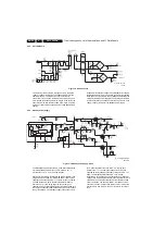
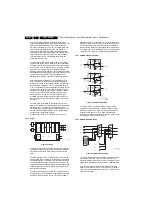
9.3.15 HOP Tint Control
Figure 9-22 HOP tint control
IC 7510 amplifies the U signal while 7520 amplifies the V
signal. The Tint control voltage changes the balance between
the U and V signals to change, causing the tint of the picture to
change.
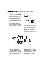
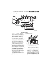
9.3.16 HOP RGB Amplifiers
Figure 9-23 HOP RGB amplifiers
The output of 7600 is fed to the RGB amplifiers before being
fed to the CRTs. Transistors 7720 and 7721 buffer the Blue
output on pin 42. The B-BIAS control voltage controls the gain
of this circuit. Transistor 7730 provides an additional voltage
gain for the signal.
Items 7710 and 7711 buffer the Green output from pin 41 of
7600. The G-BIAS controls the gain of the circuit.
The Red output from pin 40 of 7600 is buffered by 7700 and
7701. The R-BIAS controls the gain of the circuit.
The drive of the Red and Green outputs is compared with the
Blue drive by 7900-A. The difference signal is fed back to 7600
via the ABL line. If the Blue CRT is driven harder than the
Green and Red CRTs, the inverting input on pin 2 will become
greater than the non-inverting input on pin 3, resulting in the
output on pin 1 to go Low. The ABL line will go Low, causing
7600 to reduce the drive to all of the CRTs. This circuit prevents
the Blue tube from being over-driven.
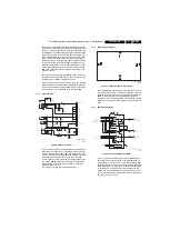
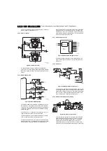
9.3.17 HOP Analogue Control
Figure 9-24 IC7800 HOP analogue control
IC 7800 develops the analogue control voltage for the HOP
panel. The I2C bus controls the IC. This IC is located on the
HOP panel.
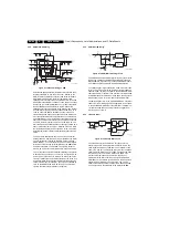
9.3.18 CRT Panel
Figure 9-25 RGB amplifiers on CRT panel
The Red, Green, and Blue signals from the HOP panel are fed
to their respective CRT panel. The signal is fed to the emitter of
7200 and then to 7202 on each panel. The output of 7202 is fed
to pin 2 of 7201, which drives the cathode of the CRT. AKB
drive is output on pin 7 and fed to the HOP panel.
9.3.19 HOP Sync Switching and Processing
Figure 9-26 HOP sync processing
Horizontal and Vertical Sync from the SSB is fed to the HOP
panel via the SSM panel, when NTSC is used as the signal
source. In sets with the D Shell RGB input, 7110 switches
between the Vertical and Horizontal Sync on the cinch
connectors or the Sync from Pins 13 and 14 of the D Shell
connector. IC 7210 selects between the output of 7110 and the
E_15000_090.eps
181004
E_15000_091.eps
181004
E_15000_092.eps
181004
E_15000_093.eps
181004
E_15000_094.eps
181004
Содержание DPTV565 AA
Страница 27: ...Circuit Diagrams and PWB Layouts 27 DPTV565 AA 7 Layout SSB Top Side E_15000_133 eps 191004 8204 000 6507 3 ...
Страница 29: ...Circuit Diagrams and PWB Layouts 29 DPTV565 AA 7 Layout SSB Bottom Side E_15000_134 eps 191004 8204 000 6507 3 ...
Страница 41: ...Circuit Diagrams and PWB Layouts 41 DPTV565 AA 7 Layout SSM Part 1 Bottom Side F_15020_011a eps 110305 Part 1 ...
Страница 42: ...42 DPTV565 AA 7 Circuit Diagrams and PWB Layouts Layout SSM Part 2 Bottom Side Part 2 F_15020_011b eps 110305 ...
Страница 43: ...Circuit Diagrams and PWB Layouts 43 DPTV565 AA 7 Layout SSM Part 3 Bottom Side F_15020_011c eps 110305 Part 3 ...
Страница 44: ...44 DPTV565 AA 7 Circuit Diagrams and PWB Layouts Layout SSM Part 4 Bottom Side F_15020_011d eps 110305 Part 4 ...
Страница 72: ...72 DPTV565 AA 7 Circuit Diagrams and PWB Layouts Personal Notes E_06532_013 eps 131004 ...
Страница 119: ...Revision List EN 119 DPTV565 AA 11 11 Revision List Manual xxxx xxx xxxx 0 First release ...

