Circuit Descriptions, List of Abbreviations, and IC Data Sheets
EN 84
DPTV565 AA
9.
9.3.4
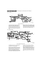
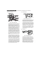
SSB Video Switching
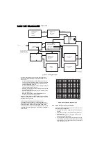
Figure 9-11 Video switching on SSB
Selected composite video from the SSM is fed to the HIP 7323,
located on the SSB. IF from the main Tuner, located on the
SSM, is fed to the SSB via connector 1020 to the switchable
SAW filters 1408 and 1410. Refer to Figure "SAW filter
switching circuit" for description of the SAW circuits. IF from the
SAW filters is then fed to Pins 2 and 3 of 7323. composite Video
is output on pin 10 and is buffered by 7411. Video is then fed to
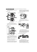
the switchable Sound traps. Refer to Figure "Sound trap
switching circuit" for a description of the Sound Traps. Output
from the Sound traps is buffered by 7322 and fed to pin 14 of
7323. IC 7323 then selects between the Tuner Video and
selected composite Video or Luminance from the SSM on pin
20. If the signal selected is composite video, it is output on pin
26 and buffered by 7320. It is then fed to the Three Line Comb
filter, 7307. Luminance is output on pin 14 and fed back to 7323
on pin 28. Chroma is output on pin 16 and fed to pin 29. The
internal Chroma switch selects between the output of the Comb
filter or external Chroma on pin 21. Selected Chroma is fed to
the internal Demodulator, which outputs UV to the YUV switch.
Selected Luminance is fed to the internal Delay and to the YUV
switch.
The YUV switch selects between the YUV from the internal
decoder and YUV from the YPbPr inputs located on the SSM.
The microprocessor, located on the SSB, via the I2C buss,
SDA-F and SCL-F, controls the HIP 7323. The YPbPr signals
for NTSC are fed through buffer amplifiers on the SSM before
being fed to the SSB. The selected YUV signal is output on
Pins 49, 50, and 51 to the PIP/DW circuit via connector 1682.
The Y or Luminance signal is fed to the internal Sync Separator
to develop Line and Frame sync. This sync is output on pin 60
and 61. pin 60 is the Line sync while pin 61 is the Frame sync.
Line sync is also output on pin 59 to synchronize the Three Line
Comb filter. When the Component input is selected by the YUV
switch (a DVD player for example), the Y signal is selected by
7017 on the SSM and fed to pin 20 of 7323. The selected Y
signal is then fed to the internal Sync Separator.
9.3.5
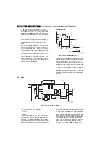
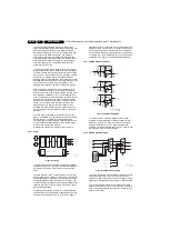
SAW Filter Switching
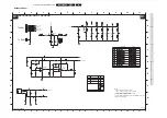
Figure 9-12 SAW filter switching circuit
The HDR2K3 AP set has a Multi-System tuning system. Since
NTSC uses a 6 MHz bandwidth and PAL/SECAM uses an 8
MHz bandwidth, it is necessary to have separate SAW filters.
The LMN line switches between PAL/SECAM and NTSC.
The LMN line goes "high" in the NTSC mode. Transistor 7405
turns "on" causing a short at the junction of resistor 3406 and
capacitor 2406, removing the signal to the PAL/SECAM SAW
filter (item 1408-A). Transistor 7401 is turned "off". Diode 6402
is forward biased via resistors 3410 and 3406, causing signal
to be applied to pin 2 of 1410-A, and the NTSC SAW filter.
The LMN line goes "low" in the PAL/SECAM mode. Transistor
7405 turns "off", allowing signal to be applied to pin 2 of 1408-
A, the PAL/SECAM SAW filter. Transistor 7401 is biased "on"
via resistors 3409 and 3407. This prevents the signal from
reaching pin 2 of 1410-A.
9.3.6
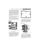
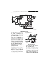
3D Comb Filter
Figure 9-13 3D Comb filter circuit
The 3D Comb Filter is used in NTSC only sets. This is a
separate PC board, which plugs into the System board. The
video signal is buffered by 7008 and 7009. Transistors 7010,
7015, 7016, and 7017 separate the Sync from the composite
video. The Sync is fed to pin 76 of 7023. The composite video
is buffered by 7011 and fed to a 6 MHz filter, 5006. This
prevents any high frequency signals from causing any
problems with the A/D conversion. The signal from 5006 is
buffered by 7012 and fed to pin 88 of 7023. A full frame 3D YC
separation is performed by the YCS circuit. The Y and C
signals are buffered and fed to 6 MHz filters, 5003 and 5004.
The YC signals are then fed back to the SSB via the SSM.
E_15000_076.eps
181004
E_15000_077.eps
181004
E_15000_078.eps
181004
Содержание DPTV565 AA
Страница 27: ...Circuit Diagrams and PWB Layouts 27 DPTV565 AA 7 Layout SSB Top Side E_15000_133 eps 191004 8204 000 6507 3 ...
Страница 29: ...Circuit Diagrams and PWB Layouts 29 DPTV565 AA 7 Layout SSB Bottom Side E_15000_134 eps 191004 8204 000 6507 3 ...
Страница 41: ...Circuit Diagrams and PWB Layouts 41 DPTV565 AA 7 Layout SSM Part 1 Bottom Side F_15020_011a eps 110305 Part 1 ...
Страница 42: ...42 DPTV565 AA 7 Circuit Diagrams and PWB Layouts Layout SSM Part 2 Bottom Side Part 2 F_15020_011b eps 110305 ...
Страница 43: ...Circuit Diagrams and PWB Layouts 43 DPTV565 AA 7 Layout SSM Part 3 Bottom Side F_15020_011c eps 110305 Part 3 ...
Страница 44: ...44 DPTV565 AA 7 Circuit Diagrams and PWB Layouts Layout SSM Part 4 Bottom Side F_15020_011d eps 110305 Part 4 ...
Страница 72: ...72 DPTV565 AA 7 Circuit Diagrams and PWB Layouts Personal Notes E_06532_013 eps 131004 ...
Страница 119: ...Revision List EN 119 DPTV565 AA 11 11 Revision List Manual xxxx xxx xxxx 0 First release ...

