Mechanical Instructions
EN 7
DPTV565 AA
4.
4.1.1
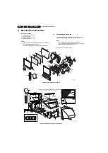
Lower Center Back Cover Removal (86)
1.
Remove all screws (B and C).
2.
Remove the Lower Center Back Cover.
4.1.2
Side Back Cover Removal
Remove all screws (F) from each of the Side Back Covers
(some prying may be necessary to dislodge covers).
Note: This allows access to the Side Jack Panel and to the Left
and the Right Speakers.
4.1.3
Large Signal Board Removal (LSB)
Note: See for the location of the panels figure "PWB location"
in Chapter 1 "Technical Specifications, Connection Facilities,
and Chassis Overview".
1.
Disconnect all cables.
2.
Remove three screws from the center of the PWB and pull
three tabs on the right of the bracket.
3.
Lift the right side of the LSB and slide the panel up and out.
4.1.4
AC Input Panel Removal
1.
Disconnect all cables.
2.
Remove four screws from the PWB.
3.
Lift the AC Input Panel up and out.
4.1.5
Small Signal Module Removal (SSM)
1.
Remove three screws along the rear of the chassis frame.
2.
Remove two screws, which hold the chassis frame and are
located between the LSB and SSB panels.
3.
Remove one screw, which holds the chassis frame and is
located between the Input Power and LSB panels
4.
Remove the rear Jack Panel cover (76).
5.
Slide the Chassis assembly rearward to allow access to the
Module Bracket.
6.
Remove the screws, which secure the Module Bracket,
and release the cables.
7.
Remove two screws from the centre of the SSM PWB.
8.
Pull three tabs on the right of the panel bracket.
9.
Lift the right side of the SSM, then move the SSM to the
right to remove it.
4.1.6
Side Jack Panel Removal
1.
Remove the Left Side Back Cover (see procedure above
excluding the Module Bracket removal).
2.
Remove two screws from the panel.
3.
Slide the Side Jack Panel PWB out of the bracket.
4.1.7
Small Signal Board Removal (SSB)
First, remove the Module Bracket (see the chapter “Small
Signal Module Removal”).
1.
Release the metal retainer clips, located at the front and
rear edges of the SIMM connector.
2.
Tilt the SSB to the right and then pull it up.
4.1.8
Convergence Panel Removal (ACS)
First, remove the Module Bracket (see the chapter “Small
Signal Module Removal”).
1.
Carefully pull the ACS panel upward to separate it from the
SSM connectors.
2.
Disconnect the cable assemblies.
4.1.9
Wide Band Video Panel Removal (HOP)
First, remove the Module Bracket (see the chapter “Small
Signal Module Removal”).
1.
Remove the rear Jack Panel cover (76).
2.
Disconnect the ribbon cable connectors.
3.
Carefully separate the HOP panel from the SSM
connectors.
4.1.10 Front Control Panel and Left or Right Speaker Removal (5)
1.
Remove the Left and Right Side Back Covers.
2.
Remove the two screws (on either side) of the speaker
location.
3.
Release two tabs on either side of the speaker baffle and
pull the baffle forwards.
4.
Loosen the ribbon cable and the grounding wire to allow
working space.
5.
Remove two screws to remove the Front Control Panel
(4527).
6.
Remove four screws each to remove the speakers (5208/
5206).
4.1.11 Upper Back Cover Removal (4)
1.
Remove all screws (A and B).
2.
Lift the cover up to dislodge from pegs (J) and remove the
cover.
4.1.12 Plastic Light Barrier Removal (Optical Assembly)
Remove two screws (E) (one each at either end of the plastic
light barrier).
4.1.13 Mirror Mounting Board Removal (57)
Remove all screws, located in the mirror mounting board
brackets, and remove the board.
Note: Take care not to place fingerprints or smudges on the
mirror.
4.1.14 Complete Optical Assembly or Individual CRT Assembly
Removal
1.
Remove the Plastic Light Barrier.
2.
Disconnect the CRT panels, 2nd anode leads (at HVT),
and the yoke connectors from assemblies to be removed.
3.
To remove the complete Optical Assembly, remove four
screws (G) and lift the assembly up and out.
4.
To remove individual CRT assemblies, remove four screws
(H) from the desired assembly and lift the assembly up and
out.
Caution: Do not disturb the focus assembly wing nuts, as this
will misadjust mechanical focus.
Содержание DPTV565 AA
Страница 27: ...Circuit Diagrams and PWB Layouts 27 DPTV565 AA 7 Layout SSB Top Side E_15000_133 eps 191004 8204 000 6507 3 ...
Страница 29: ...Circuit Diagrams and PWB Layouts 29 DPTV565 AA 7 Layout SSB Bottom Side E_15000_134 eps 191004 8204 000 6507 3 ...
Страница 41: ...Circuit Diagrams and PWB Layouts 41 DPTV565 AA 7 Layout SSM Part 1 Bottom Side F_15020_011a eps 110305 Part 1 ...
Страница 42: ...42 DPTV565 AA 7 Circuit Diagrams and PWB Layouts Layout SSM Part 2 Bottom Side Part 2 F_15020_011b eps 110305 ...
Страница 43: ...Circuit Diagrams and PWB Layouts 43 DPTV565 AA 7 Layout SSM Part 3 Bottom Side F_15020_011c eps 110305 Part 3 ...
Страница 44: ...44 DPTV565 AA 7 Circuit Diagrams and PWB Layouts Layout SSM Part 4 Bottom Side F_15020_011d eps 110305 Part 4 ...
Страница 72: ...72 DPTV565 AA 7 Circuit Diagrams and PWB Layouts Personal Notes E_06532_013 eps 131004 ...
Страница 119: ...Revision List EN 119 DPTV565 AA 11 11 Revision List Manual xxxx xxx xxxx 0 First release ...


