Circuit Descriptions, List of Abbreviations, and IC Data Sheets
EN 89
DPTV565 AA
9.
Sync from the SSB. For separate Horizontal and Vertical Sync,
the output of 7210 is fed to the multiplexer IC 7330, which is
used as a switch. In the case of Sync on Y or Sync on Green,
pin 19 of 7210 is fed to pin 18 of 7210 to a Sync Separator. If
separate Horizontal Sync is present, the internal detector in
7210 turns the Sync Separator "off". The Sync output on pin 17
is fed to a Low Pass Filter, which separates the Vertical Sync.
The Timer IC 7328 detects the Horizontal Sync and feeds it to
7330. The detected Horizontal Sync from 7328 is fed to pin 1 of
7330 to switch the IC to the pin 6 and 3 inputs.
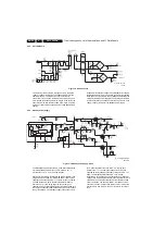
9.3.20 Line Output
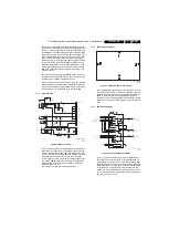
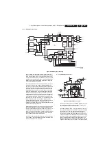
Figure 9-27 Line output circuit
Horizontal drive from the HOP panel is fed to 7807 on the Large
Signal panel. Transistor 7807 drives the Horizontal Output
Transistor 7801, which drives the Yokes and the Horizontal
Output Transformer 5801. Transformer 5801 produces plus
and minus 13-Volt supplies for the Vertical Output circuit. It also
produces a 200-Volt source and Filament voltage for the CRT
panels. The output of 7807 also drives 7803 and 7802, which
drives the Dynamic Focus circuit.
9.3.21 Frame Amplifier
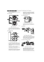
Figure 9-28 Frame circuit
The Vertical drive from the HOP panel drives the Vertical
Output IC 7811. This IC is located on the Large Signal panel.
Drive is fed to pin 7 and is output on pin 5 to drive the three
Vertical Yokes. This IC is powered by the plus and minus 13-
Volt supplies from the Horizontal Output circuit. A Vertical pulse
on pin 6 is fed to the sweep failure detection circuit. If there is
a failure in the Horizontal or Vertical sweep, the High Voltage
will be shut down.
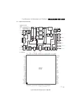
E_15000_095.eps
181004
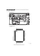
E_15000_096.eps
181004
Содержание DPTV565 AA
Страница 27: ...Circuit Diagrams and PWB Layouts 27 DPTV565 AA 7 Layout SSB Top Side E_15000_133 eps 191004 8204 000 6507 3 ...
Страница 29: ...Circuit Diagrams and PWB Layouts 29 DPTV565 AA 7 Layout SSB Bottom Side E_15000_134 eps 191004 8204 000 6507 3 ...
Страница 41: ...Circuit Diagrams and PWB Layouts 41 DPTV565 AA 7 Layout SSM Part 1 Bottom Side F_15020_011a eps 110305 Part 1 ...
Страница 42: ...42 DPTV565 AA 7 Circuit Diagrams and PWB Layouts Layout SSM Part 2 Bottom Side Part 2 F_15020_011b eps 110305 ...
Страница 43: ...Circuit Diagrams and PWB Layouts 43 DPTV565 AA 7 Layout SSM Part 3 Bottom Side F_15020_011c eps 110305 Part 3 ...
Страница 44: ...44 DPTV565 AA 7 Circuit Diagrams and PWB Layouts Layout SSM Part 4 Bottom Side F_15020_011d eps 110305 Part 4 ...
Страница 72: ...72 DPTV565 AA 7 Circuit Diagrams and PWB Layouts Personal Notes E_06532_013 eps 131004 ...
Страница 119: ...Revision List EN 119 DPTV565 AA 11 11 Revision List Manual xxxx xxx xxxx 0 First release ...


