


AN4536 Application Note Rev. 2.0 1/2014
Freescale Semiconductor
33
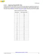
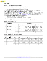
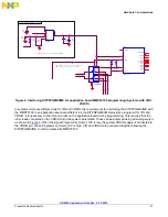
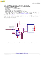
Hardware Considerations
3.4
Programming using a Generic Programmer
Following are the requirements if it is preferred to use a generic programmer board:
1.
VIN power supply: 3.3 V, 100 mA
2.
VDDIO power supply: 1.8 V to 3.3 V, 10 mA
3.
I
2
C Master
4.
GPO signal to control MMPF0100's PWRON pin
5.
GPO signal to control analog switch (Programmer_Select_O/P)
6.
9.5 V/9.25 V 100 mA power supply at VDDOTP bypassed by 2 x 10
μ
F capacitors. The voltage depends
on the silicon revision used. See section
OTP Programming Example
for details.
An example is shown in
Figure 6
.
Note: Using the analog switch may not be the most cost effective option to isolate the I
2
C bus. Similar functionality
can be achieved by using solder shorts or 0 Ohm resistors. However, minor rework of the board would be required
once OTP programming is completed.
Figure 6. Interfacing a Generic Programmer to the MMPF0100 in an Application Board
Optional isolation
diode to prevent
VDDIO supply from
being over loaded
Processor_SCL
Processor_SDA
Pro
g
ra
m
m
e
r_
SCL
Pro
g
ra
m
m
e
r_
SDA
Program
m
e
r_Selec
t_O/P
SYSTEM_VDDIO_SUPPLY
Pro
g
ra
m
m
e
r_
VDDIO
Pro
g
ra
m
m
e
r_
VIN
Pro
g
ra
m
m
e
r_
PW
RON
R95
4.7K
R96
4.7K
MMPF0100/Z
U15A
ICTEST
5
INTB
1
RESETBMCU
3
SCL
54
SDA
53
SDWNB
2
STANDBY
4
VCOREDIG
51
VCOREREF
52
VDDIO
55
VDDOTP
47
PWRON
56
VCORE
49
GNDREF
48
VIN
50
NLAS3158
1
2
3
5
4
12
11
9
6
8
7
10
DIODE
A
C