


AN4536 Application Note Rev. 2.0 1/2014
Freescale Semiconductor
31
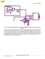
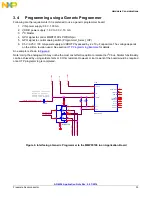
Hardware Considerations
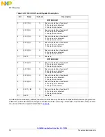
Figure 4. Interfacing KITPFPGMEVME for application board MMPF0100 programming (Systems with VIN =
VDDIO)
In systems which use different rails for VIN and VDDIO, the requirements for interfacing the KITPFPGMEVME with
the MMPF0100 in an application board are different. As the KITPGPGMEVME provides a single rail for VIN and
VDDIO, it is necessary to short the two rails on the application board during programming. This requires that the
other loads connected on the VDDIO rail in the system be isolated. These can be achieved using an analog switch
as shown in
Figure 5
. When the signal Programmer_Select_O/P is low, the system VDDIO supply is connected to
the VDDIO pin. When Programmer_Select_O/P is high, VIN and VDDIO are connected together allowing the
KITPFPGMEVME to communicate with MMPF0100.
3.3V Regulator from KITPFPGMEVME
LDO REGULATOR 3.3V
R1
R2
Optional isolation to prevent
LDO from being over loaded
Processor_SCL
Processor_SDA
Pro
g
ra
m
m
e
r_
SCL
Pro
g
ra
m
m
e
r_
SDA
Program
m
e
r_Selec
t_O/P
3V3
3V3EN
INPUT
3V3
0
0
0
0
R99
4.7K
C92
470PF
R102
12.0K
R103
0
C94
1.0UF
+
C95
2.2UF
R100
4.7K
C93
2.2uF
DNP
R101
20K
NLAS3158
1
2
3
5
4
12
11
9
6
8
7
10
U21
MIC5205
IN
1
GND
2
ADJ
4
EN
3
OUT
5
MMPF0100/Z
U19A
ICTEST
5
INTB
1
RESETBMCU
3
SCL
54
SDA
53
SDWNB
2
STANDBY
4
VCOREDIG
51
VCOREREF
52
VDDIO
55
VDDOTP
47
PWRON
56
VCORE
49
GNDREF
48
VIN
50