NXP Semiconductors
Quick start ADC1412D, ADC1212D, ADC1112D series
Quick start
QS_ADC1412D_7.doc
© NXP B.V. 2010. All rights reserved.
Rev. 7 — 6 August 2010
18 of 41
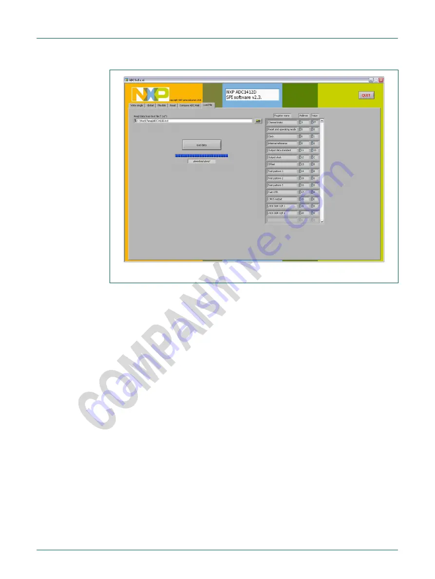
Fig 16. SPI main window: load file page, successful download performed
Страница 1: ...ev 7 6 August 2010 Quick start Document information Info Content Keywords PCB2004 1 Demonstration board ADC Converter ADC1412D ADC1212D and ADC1112D series Abstract This document describes how to use the demonstration board for the analog to digital converter ADC1412D ADC1212D and ADC1112D series Overview ...
Страница 2: ...evision history Rev Date Description 1 20081001 Initial version 2 20090518 Update to PCB2004 1 2 3 20090610 Add SPI software description 4 20100518 Update to latest release of SPI software Add HSDC extension module acquisition system description 5 20100601 Correction added 6 20100730 Update for LVDS acquisition mode 7 20100806 Update to latest acquisition software tool ...
Страница 3: ... GND POWER SUPPLY I 40 mA GND 1 8V LOGIC ANALYZER Output data ADC A top to bottom DA13 MSB to DA0 LSB CLOCK SIGNAL sinewave AC SYNTHESIZED SIGNAL GENERATOR USB SPI MODULE INPUT B SIGNAL 2Vpp sinewave AC SYNTHESIZED SIGNAL GENERATOR INPUT A SIGNAL 2Vpp sinewave AC SYNTHESIZED SIGNAL GENERATOR FILTER High order Band pass FILTER High order Band pass PRESENTED CONFIGURATION 2Vpp input full scale Singl...
Страница 4: ...D 1 8V LOGIC ANALYZER Output data ADC A top to bottom DA11 MSB to DA0 LSB CLOCK SIGNAL sinewave AC SYNTHESIZED SIGNAL GENERATOR USB SPI MODULE INPUT B SIGNAL 2Vpp sinewave AC SYNTHESIZED SIGNAL GENERATOR INPUT A SIGNAL 2Vpp sinewave AC SYNTHESIZED SIGNAL GENERATOR FILTER High order Band pass FILTER High order Band pass PRESENTED CONFIGURATION 2Vpp input full scale Single Sine wave clock signal Inp...
Страница 5: ...D 1 8V LOGIC ANALYZER Output data ADC A top to bottom DA10 MSB to DA0 LSB CLOCK SIGNAL sinewave AC SYNTHESIZED SIGNAL GENERATOR USB SPI MODULE INPUT B SIGNAL 2Vpp sinewave AC SYNTHESIZED SIGNAL GENERATOR INPUT A SIGNAL 2Vpp sinewave AC SYNTHESIZED SIGNAL GENERATOR FILTER High order Band pass FILTER High order Band pass PRESENTED CONFIGURATION 2Vpp input full scale Single Sine wave clock signal Inp...
Страница 6: ...t Analog ground 1 5 Input signals IN CLK The input clock signal can be either a sinewave or a LVCMOS signal To ensure a good evaluation of the device the input signal and the input clock must be synchronized together Moreover the input frequency Fi MHz and the clock frequency Fclk Msps should follow the formula known as coherency criteria for FFT processing see section 3 6 where M is an odd number...
Страница 7: ... clock DAV is provided by the device for the data acquisition Table 3 Output signals Name Function View J5 Array connector ADC A digital output DA0 to DA13 Out of range signal OTRA J6 Array connector ADC B digital output DB0 to DB13 and Data Valid DAV 1 7 SPI Mode The ADC1412D can be controlled either by a Serial Peripheral Interface SPI or by PIN Table 4 SPI Interface Name Function View J9 Array ...
Страница 8: ...e connected to your PC it will display the following screen It automatically detects the resolution Fig 5 SPI main window successfully detect ADC1412D series The main application will display the panel to drive the ADC1412D as described in the following section All devices ADC1412D ADC1212D or ADC1112D series can be controlled in same way The following shows only example for ADC1412D series howeve...
Страница 9: ...7 SPI main window write page This can be done by either Selecting the register with its name then enter the byte value by default in hexadecimal and then press the send button referred as above Or enter the address of the register as defined in the datasheet then enter the byte value Global and then press the send button referred as above 1 8 2 2 Page Global This page allows getting access to the ...
Страница 10: ...All rights reserved Quick start Rev 7 6 August 2010 10 of 41 Fig 8 SPI main window global page Perform any settings and then click on the send button to update the ADC1412D registers 1 8 2 3 Page Flexible This page allows getting access to the bit definition of remaining registers as defined in the datasheet ...
Страница 11: ...S_ADC1412D_7 doc NXP B V 2010 All rights reserved Quick start Rev 7 6 August 2010 11 of 41 Fig 9 SPI main window flexible page Perform any settings and then click on the send button to update the ADC1412D registers 1 8 2 4 Page Read This page allows reading the ADC1412D registers ...
Страница 12: ...e on field the value will be automatically displayed in field value in hexadecimal by default or all the bank of registers click on the read all button this will automatically update the table in field When all registers have been read it is possible to save the data to a text file The settings are saved in a table like format as shown below Table 5 Typical saving on text file Content of file is s...
Страница 13: ...DS DDR O P 1 21 0 LVDS DDR O P 2 22 0 Note that all data are saved in hexadecimal format Click on the save to file button this will display a window to select the file to store data to Fig 11 SPI main window read page select file to save data to dialog box Make sure that you store your file with txt extension this will allow you to re use the file on the Load file page 1 8 2 5 Page Compare ADC A B...
Страница 14: ...ev 7 6 August 2010 14 of 41 Fig 12 SPI main window compare ADC A B page To do the comparison follow the procedure below Select the first register and last register to be compared buttons and Click on compare button the table will show the values of all registers in the field of comparison for both ADC A and B A typical example is given below ...
Страница 15: ...Fig 13 SPI main window compare ADC A B page comparison result example Click on the save to file button to save the result of the comparison this will display a window to select the file to store data to Fig 14 SPI main window compare ADC A B page select file to save data to dialog box The format of the text file is equivalent to the previous section and is given below ...
Страница 16: ...e is shown as table format Column 1 Column 2 Column 3 Register Name ADC A ADC B Channel index 1 2 Reset and operating mode 0 0 Clock 1 1 Internal reference 0 0 Output data standard 10 10 Output clock C C Offset 0 0 Test pattern 1 0 0 Test pattern 2 0 0 Test pattern 3 0 0 Fast OTR 0 0 CMOS output E E LVDS DDR O P 1 0 0 LVDS DDR O P 2 0 0 1 8 2 6 Page Load file This page allows downloading configura...
Страница 17: ...e only restriction is regarding the formatting of the file as given in section 1 5 2 4 Note this page can not be used to download data saved during the comparison process To download settings onto ADC1412D registers follow the procedure below Browse to select your file button Click on load data button A message on field and a progress bar will inform about the status of the operation until message...
Страница 18: ...s Quick start ADC1412D ADC1212D ADC1112D series Quick start QS_ADC1412D_7 doc NXP B V 2010 All rights reserved Quick start Rev 7 6 August 2010 18 of 41 Fig 16 SPI main window load file page successful download performed ...
Страница 19: ...MOD01 DB acquisition board Fig 17 HSDC extension module acquisition board 5V POWER SUPPLY I 3 2A REFERENCE SIGNAL typical 10MHz SIGNAL GENERATOR USB SPI MODULE PRESENTED CONFIGURATION acquisition board external reference signal LVDS DDR 16 bit input stream CMOS 2 16 bit channels input LVDS DDR I O CONNECTOR up to 325MHz 16 bit LVDS DDR CMOS I O CONNECTOR 2 channels up to 200MHz 16 bit JUMPER FOR I...
Страница 20: ...r external reference for signal generation In this section the specific requirement for the use with ADC1412D demo board will be shown For more details on the HSDC EXTMOD01 DB please contact dataconverter support nxp com 2 1 HSDC extension module hardware initialization Before using the generation board make sure that you connect the USB cable prior to the supply 2 2 HSDC extension module software...
Страница 21: ... 41 Fig 19 USBConfigSetup window step 2 Click Next to continue Fig 20 USBConfigSetup window step 3 Click Next to finish the installation process The system is now ready to use the ADC1412D series board for evaluation purpose 2 3 HSDC extension module CMOS connector description The figure 21 shows a brief description of the hardware connection on the HE14 connector ...
Страница 22: ...t 2010 22 of 41 Fig 21 HSDC extension module HE14 CMOS hardware schematic overview The HSDC extension module can acquire data in CMOS level using either the on board clock generated by the internal PLL refer to as pDFS_CLK 0 nDFS_CLK 0 that will be used by the FPGA In this case the reference of the board should be delivered by the clock signal generator ...
Страница 23: ...C refer to as P1_CLK_IN This is the preferred situation since the user will not deal with any set up hold timing for the acquisition Refer to section 3 3 for software configuration 2 4 HSDC extension module LVDS DDR connector description The figure 22 shows a brief description of the hardware connection on the SAMTEC connector Fig 22 HSDC extension module SAMTEC LVDS DDR hardware schematic overvie...
Страница 24: ... Falling edge as shown below Fig 24 HSDC extension module LVDS DDR interleaved data bit falling edge acquired The HSDC extension module can acquire data in LVDS DDR using either the on board clock generated by the internal PLL refer to as pDFS_CLK 0 nDFS_CLK 0 that will be used by the FPGA In this case the reference of the board should be delivered by the clock signal generator or the clock provid...
Страница 25: ... with CMOS outputs configuration for which connection is straightforward together with a supply extension module release A for the ADC1412D demo board Fig 25 Evaluation set up measurement with ADC1412D CMOS and HSDC extension module USB SPI MODULE PRESENTED CONFIGURATION Single ended clock on CLKP 2 Vpp input full scale Binary CMOS outputs CLOCK SIGNAL e g 125 Msps CLOCK GENERATOR REFERENCE SIGNAL...
Страница 26: ...or the ADC1412D demo board Fig 26 Evaluation set up measurement with ADC1412D LVDS and HSDC extension module Note 1 make sure that supply extension release B is used it delivers the 3 V supply for LVDS output path for the ADC Note 2 make sure that LVDS connection is done as shown USB SPI MODULE PRESENTED CONFIGURATION Single ended clock on CLKP 2 Vpp input full scale Binary LVDS outputs CLOCK SIGN...
Страница 27: ...th the appropriate bin file provided on the CD located at 5 CGAP Software Install CGAP FPGA bin v03 Among the 8 files 2 are considered here cgap_v03_P1C_RE_3V3_GEN bin the FPGA will use the rising edge of the clock delivered by the P1 connector This is suitable when using CMOS use case cgap_v03_P2C_RE_3V3_ACQ bin the FPGA will use the rising edge of the clock delivered by the P1 connector This is ...
Страница 28: ...ash used Click Update this should display 6 green check boxes and the value of the corresponding frequency being actually generated by the board If one or several red cross appear check that the clock signal coming from P1 or P2 is correctly provided to the board The Data Phase Shift allows the user to shift the clock position wrt data by the amount of time indicated Note you can edit the LMK file...
Страница 29: ...th bit of the HSDC extension module Tune the fields Input is located on file B between xx MSB and xx LSB to describe this configuration see figure 29 Fig 29 USB Configurator window pattern acquisition for ADC1412D series 3 5 1 2 Use case ADC1212D series The hardware connection between the ADC1212D series and the HSDC extension module has to be described to get correct results This is done by using...
Страница 30: ...here ADC MSB is connected to the 14 th bit and ADC LSB is connected to the 4 th bit of the HSDC extension module Tune the fields Input is located on file A between xx MSB and xx LSB to describe this configuration see figure 31 The channel 1 receives the data from ADC channel A top ADC where ADC MSB is connected to the 1 st bit and ADC LSB is connected to the 11 th bit of the HSDC extension module ...
Страница 31: ... to schematics for more details A refers to ADCA B refers to ADCB Case 1 LVDS DDR data bit wise DAV inverted default mode Fig 32 HSDC extension module LVDS DDR data bit wise DAV inverted data path Case 2 LVDS DDR data byte wise DAV inverted Fig 33 HSDC extension module LVDS DDR data byte wise DAV inverted data path In order to do the acquisition the number of samples needs to be filled in the Patt...
Страница 32: ...112D series see figure 9 for proper settings LVDS is set DAV is inverted and tap 5 chosen 3 5 3 Pattern acquisition Browse on both channel path configuration to select the file to store the data that will be acquired Click on Acquire and Save buttons to end the capture process 3 6 FFT post processing Once acquisition is done the captured data can now be processed for FFT results using the NXP_ADC_...
Страница 33: ...nput and clock frequency Indicate whether it is CMOS or LVDS DDR bit wise or LVDS DDR byte wise mode 3 6 2 Acquisition software frequency indication The second step consists in indicating the relevant numbers for the FFT processing the resolution N 14 in this case the input frequency Fin 170 MHz in our example the sampling frequency Fs 125 Msps in our example whether Fin or Fs are coherent or not ...
Страница 34: ...FT results display Press the COMPUTE button to display the results from the FFT processing The results fields will be updated depending on the number of input files If 2 files have been processed it is possible to display both results on the same picture for all graphs using the Display button Display ADC1 or Display ADC2 or Display ADC1 ADC2 3 6 3 1 FFT spectrum The first graph to be displayed is...
Страница 35: ...e tables and give the relevant dynamic parameters Table first 6 harmonics frequencies and amplitude level Table dynamics parameters ENOB expressed in bit Level of the digital output signal relative to the full scale SINAD in dBc THD in dBc calculated over first 6 harmonics SNR in dBc and dBFS SFDR in dBc and dBFS 3 6 3 2 Reorganized signal The Reorganized signal displays the reconstructed sine wav...
Страница 36: ...ick start Rev 7 6 August 2010 36 of 41 Fig 38 NXP_ADC_Acquisition window reorganized signal Press the Autoscale button to display the whole content 3 6 3 3 Unreconstruted signal The unreconstructed signal displays the unreconstructed sine wave corresponding to the whole number of period being acquired following the coherency rule ...
Страница 37: ...Fig 39 NXP_ADC_Acquisition window unreconstruted signal Press the Autoscale button to display the whole content Use the zoom tool to observe in more details all the captured data 3 6 3 4 Histogram The histogram graph shows the distribution of output codes This graph allows to know which code is present and if there is any missing code in the conversion range Zoom tool ...
Страница 38: ... series Quick start QS_ADC1412D_7 doc NXP B V 2010 All rights reserved Quick start Rev 7 6 August 2010 38 of 41 Fig 40 NXP_ADC_Acquisition window code histogram Press the Autoscale button to display the whole content The table shows the range of output codes ...
Страница 39: ...e chosen such that it follows the equation above To do this iterative calculation one has to decide whether Fin or Fs is fixed To illustrate this process let s consider our current example with Fin 170 MHz Fs 125 Msps and N 16384 samples acquired if Fin is fixed this leads to M 36863 periods of input signal to be acquired and a real sampling frequency to be Fs 124 995737 MHz if Fs is fixed this le...
Страница 40: ...412D ADC1212D ADC1112D series Quick start QS_ADC1412D_7 doc NXP B V 2010 All rights reserved Quick start Rev 7 6 August 2010 40 of 41 5 Notes For any question feel free to contact us at the following e mail dataconverter support nxp com ...
Страница 41: ...e ADC A B 13 1 8 2 6 Page Load file 16 2 HSDC extension module acquisition board 19 2 1 HSDC extension module hardware initialization 20 2 2 HSDC extension module software initialization 20 2 3 HSDC extension module CMOS connector description 21 2 4 HSDC extension module LVDS DDR connector description 23 3 Combo ADC1412D and HSDC extension module 25 3 1 ADC1412D CMOS outputs 25 3 2 ADC1412D LVDS o...