


27
CHAPTER 4 CAUTIONS
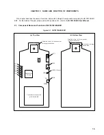
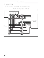
4.1
V
DD
and HV
DD
of Target System
(1) V
DD
and HV
DD
in the target system are used to operate the circuit in the emulator.
(2) When JP2 is set as 1-2 : open and 3-4 : short, the evaluation chip in the emulator operates on V
DD
and HV
DD
from the target system.
(3) When JP2 is set as 1-2 : open and 3-4 : open, the emulator recognizes the target system power is off and
operates with the 3.3 V power supply.
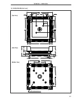
Figure 4-1. Schematic Diagram of Power Supply Flow
IE-703102-MC-EM1
I/O chip
Target system
CV
DD
V
DD
HV
DD
Relay
Power supply
circuit
Evaluation
chip
IE-703102-MC
1
2
3
4
JP2
1
2
3
4
JP2
4.2
X1 Signal
The input signal (X1 signal) from the target system is delayed (for t
pLH
= t
pHL
= 13.2 ns (MAX.)) because it passes
through VHC157 before it is input to the I/O chip of the emulator.
In addition, the DC characteristics change. The input voltage becomes V
IH
= 2.31 V (MIN.) and V
IL
= 0.99 V
(MAX.). The input current becomes I
IN
=
±
1.0
µ
A (MAX.).
Содержание IE-703102-MC-EM1
Страница 2: ...2 MEMO ...
Страница 10: ...10 MEMO ...
Страница 24: ...24 MEMO ...
Страница 26: ...26 MEMO ...
Страница 34: ...34 MEMO ...
Страница 36: ...APPENDIX A DIMENSIONS 36 2 SC 144SD Unit mm 109 144 72 37 108 1 73 36 43 13 13 40 130 43 213 46 ...
Страница 40: ...40 MEMO ...
Страница 46: ...46 MEMO ...
Страница 48: ...48 MEMO ...


