CHAPTER 4 CAUTIONS
28
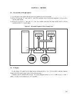
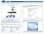
Figure 4-2. Diagram of X1 Signal Flow
I/O chip
IE-703102-MC-EM1
X1 signal
Target System
X1 pin
VHC157
4.3
Pin Termination
(1) MODE0 to MODE3 pins
When the emulator operates as a stand-alone unit, the operation mode of the emulator is single-chip mode 0.
The MODE0 to MODE3 pins are connected as follows.
•
MODE0: Connected to V
SS
via a resistor (33 k
Ω
). (Pull-down)
•
MODE1: Connected to V
DD
via a resistor (5.1 k
Ω
). (Pull-up)
•
MODE2: Unconnected
•
MODE3: Unconnected
(2) RESET pin
This pin is connected to V
DD
via a resistor (5.1 k
Ω
). (Pull-up)
(3) CKSEL pin
Pull-up/pull-down switching is possible with SW1.
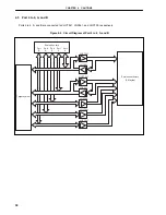
Figure 4-3. Circuit Diagram of CKSEL Pin
VHCT541
I/O chip
SW1
CKSEL
CKSEL pin
33 k
Ω
100
Ω
HV
DD
Содержание IE-703102-MC-EM1
Страница 2: ...2 MEMO ...
Страница 10: ...10 MEMO ...
Страница 24: ...24 MEMO ...
Страница 26: ...26 MEMO ...
Страница 34: ...34 MEMO ...
Страница 36: ...APPENDIX A DIMENSIONS 36 2 SC 144SD Unit mm 109 144 72 37 108 1 73 36 43 13 13 40 130 43 213 46 ...
Страница 40: ...40 MEMO ...
Страница 46: ...46 MEMO ...
Страница 48: ...48 MEMO ...


