


4- 8
M68000 8-/16-/32-BIT MICROPROCESSORS USER'S MANUAL
MOTOROLA
STATE 12
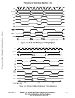
The write portion of the cycle starts in S12. The valid function codes on
FC2–FC0, the address bus lines,
AS
, and R/
W
remain unaltered.
STATE 13
During S13, no bus signals are altered.
STATE 14
On the rising edge of S14, the processor drives R/
W
low.
STATE 15
During S15, the data bus is driven out of the high-impedance state as the
data to be written are placed on the bus.
STATE 16
At the rising edge of S16, the processor asserts
L D S
or
DS
. The
processor waits for
DTACK
or
BERR
or
VPA
, an M6800 peripheral signal.
When
VPA
is asserted during S16, the cycle becomes a peripheral cycle
(refer to Appendix B M6800 Peripheral Interface). If neither termination
signal is asserted before the falling edge at the close of S16, the processor
inserts wait states (full clock cycles) until either
DTACK
or
BERR
is asserted.
STATE 17
During S17, no bus signals are altered.
STATE 18
During S18, no bus signals are altered.
STATE 19
On the falling edge of the clock entering S19, the processor negates
AS
,
L D S
, and
DS
. As the clock rises at the end of S19, the processor
places the address and data buses in the high-impedance state, and drives
R/
W
high. The device negates
DTACK
or
BERR
at this time.
4.2 OTHER BUS OPERATIONS
Refer to Section 5 16-Bit Bus Operations for information on the following items:
• CPU Space Cycle
• Bus Arbitration
— Bus Request
— Bus Grant
— Bus Acknowledgment
• Bus Control
• Bus Errors and Halt Operations
• Reset Operations
• Asynchronous Operations
• Synchronous Operations
F
re
e
sc
a
le
S
e
m
ic
o
n
d
u
c
to
r,
I
Freescale Semiconductor, Inc.
For More Information On This Product,
Go to: www.freescale.com
n
c
.
..


