


5- 34
M68000 8-/16-/32-BIT MICROPROCESSORS USER'S MANUAL
MOTOROLA
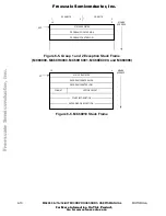
ADDR
AS
R/W
UDS/LDS
DATA
DTACK
11
17
31
28
29
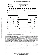
Figure 5-33. Pseudo-Asynchronous Read Cycle
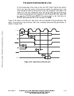
During a write cycle, after the processor asserts
AS
but before driving the data bus, the
processor drives R/
W
low. Parameter #55 specifies the minimum time between the
transition of R/
W
and the driving of the data bus, which is effectively the maximum turnoff
time for any device driving the data bus.
After the processor places valid data on the bus, it asserts the data strobe signal(s). A
data setup time, similar to the address setup time previously discussed, can be used to
improve performance. Parameter #29 is the minimum time a slave device can accept valid
data before recognizing a data strobe. The slave device asserts
DTACK
after it accepts
the data. Parameter #25 is the minimum time after negation of the strobes during which
the valid data remains on the address bus. Parameter #28 is the maximum time between
the negation of the strobes by the processor and the negation of
DTACK
by the slave
device. If
DTACK
remains asserted past the time specified by parameter #28, the
processor may recognize it as being asserted early in the next bus cycle and may
terminate that cycle prematurely. Figure 5-34 shows the important timing specifications for
a pseudo-asynchronous write cycle.
F
re
e
sc
a
le
S
e
m
ic
o
n
d
u
c
to
r,
I
Freescale Semiconductor, Inc.
For More Information On This Product,
Go to: www.freescale.com
n
c
.
..


