MOTOROLA
M68000 8-/16-/32-BIT MICROPROCESSORS USER'S MANUAL
10-27
6A
8
6
15
13
9
14
12
17
18
47
28
25
26
48
47
30
47
32
56
47
32
S0
S1
S2
S3
S4
S5
S6
CLK
FC2-FC0
A23-A0
AS
LDS / UDS
R/W
DTACK
DATA OUT
BERR / BR
(NOTE 2)
HALT / RESET
47
ASYNCHRONOUS
INPUTS
(NOTE 1)
S7
NOTES:
1. Timing measurements are referenced to and from a low voltage of 0.8 V and a high voltage of 2.0 V,
unless otherwise noted. The voltage swing through this range should start outside and pass through the
range such that the rise or fall is linear between 0.8 V and 2.0 V.
2. Because of loading variations, R/W may be valid after AS even though both are initiated by the rising edge
of S2 (specification #20A).
23
21A
7
11
11A
9
14A
53
7
55
21
22
20A
20
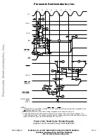
Figure 10-13. MC68EC000 Write Cycle Timing Diagram
F
re
e
sc
a
le
S
e
m
ic
o
n
d
u
c
to
r,
I
Freescale Semiconductor, Inc.
For More Information On This Product,
Go to: www.freescale.com
n
c
.
..

