background image

MOTOROLA

M68000 8-/16-/32-BIT MICROPROCESSORS USER'S MANUAL

5- 27

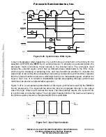
S0

S2

S4

S6

CLK

FC2–FC0

A23–A1

S0

S2

S4

S6

AS

R/W

DTACK

D0–D15

BERR

HALT

UDS

LDS

RETRY

HALT

READ

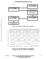
Figure 5-28. Delayed Retry Bus Cycle Timing Diagram

The processor terminates the bus cycle, then puts the address and data lines in the high-
impedance state. The processor remains in this state until 

HALT

 is negated. Then the

processor retries the preceding cycle using the same function codes, address, and data
(for a write operation). 

BERR

 should be negated at least one clock cycle before 

HALT

 is

negated.

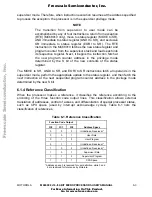
NOTE

To guarantee that the entire read-modify-write cycle runs
correctly and that the write portion of the operation is
performed without negating the address strobe, the processor
does not retry a read-modify-write cycle. When a bus error
occurs during a read-modify-write operation, a bus error
operation is performed whether or not 

HALT

 is asserted.

5.4.3 Halt Operation (

HALT)

HALT

 performs a halt/run/single-step operation similar to the halt operation of an

MC68000. When 

HALT

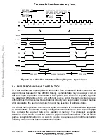
 is asserted by an external device, the processor halts and remains

halted as long as the signal remains asserted, as shown in Figure 5-29.


F

re

e

sc

a

le

 S

e

m

ic

o

n

d

u

c

to

r,

 I


Freescale Semiconductor, Inc.

For More Information On This Product,

   Go to: www.freescale.com

n

c

.

..

Содержание M68000

Страница 1: ...ponents in systems intended for surgical implant into the body or other applications intended to support or sustain life or for any other application in which the failure of the Motorola product could create a situation where personal injury or death may occur Should Buyer purchase or use Motorola products for any such unintended or unauthorized application Buyer shall indemnify and hold Motorola ...

Страница 2: ...odes 2 3 2 3 Data Organization In Registers 2 5 2 3 1 Data Registers 2 5 2 3 2 Address Registers 2 6 2 4 Data Organization In Memory 2 6 2 5 Instruction Set Summary 2 8 Section 3 Signal Description 3 1 Address Bus 3 3 3 2 Data Bus 3 4 3 3 Asynchronous Bus Control 3 4 3 4 Bus Arbitration Control 3 5 3 5 Interrupt Control 3 6 3 6 System Control 3 7 3 7 M6800 Peripheral Control 3 8 3 8 Processor Func...

Страница 3: ...ership 3 Wire Arbitration Only 5 15 5 3 Bus Arbitration Control 5 15 5 4 Bus Error and Halt Operation 5 23 5 4 1 Bus Error Operation 5 24 5 4 2 Retrying The Bus Cycle 5 26 5 4 3 Halt Operation 5 27 5 4 4 Double Bus Fault 5 28 5 5 Reset Operation 5 29 5 6 The Relationship of DTACK BERR and HALT 5 30 5 7 Asynchronous Operation 5 32 5 8 Synchronous Operation 5 35 Section 6 Exception Processing 6 1 Pr...

Страница 4: ...n From Exception MC68010 6 20 Section 7 8 Bit Instruction Timing 7 1 Operand Effective Address Calculation Times 7 1 7 2 Move Instruction Execution Times 7 2 7 3 Standard Instruction Execution Times 7 3 7 4 Immediate Instruction Execution Times 7 4 7 5 Single Operand Instruction Execution Times 7 5 7 6 Shift Rotate Instruction Execution Times 7 6 7 7 Bit Manipulation Instruction Execution Times 7 ...

Страница 5: ...nstruction Execution Times 9 2 9 3 Standard Instruction Execution Times 9 4 9 4 Immediate Instruction Execution Times 9 6 9 5 Single Operand Instruction Execution Times 9 6 9 6 Shift Rotate Instruction Execution Times 9 8 9 7 Bit Manipulation Instruction Execution Times 9 9 9 8 Conditional Instruction Execution Times 9 9 9 9 JMP JSR LEA PEA and MOVEM Instruction Execution Times 9 10 9 10 Multiprec...

Страница 6: ...s Arbitration 10 17 10 13 MC68EC000 DC Electrical Spec ifications 10 23 10 14 MC68EC000 AC Electrical Specifications Read and Write 10 24 10 15 MC68EC000 AC Electrical Specifications Bus Arbitration 10 28 Section 11 Ordering Information and Mechanical Data 11 1 Pin Assignments 11 1 11 2 Package Dimensions 11 7 Appendix A MC68010 Loop Mode Operation Appendix B M6800 Peripheral Interface B 1 Data Tr...

Страница 7: ...e Write Cycle Flowchart 4 4 4 4 Write Cycle Timing Diagram 4 4 4 5 Read Modify Write Cycle Flowchart 4 6 4 6 Read Modify Write Cycle Timing Diagram 4 7 5 1 Word Read Cycle Flowchart 5 2 5 2 Byte Read Cycle Flowchart 5 2 5 3 Read and Write Cycle Timing Diagram 5 3 5 4 Word and Byte Read Cycle Timing Diagram 5 3 5 5 Word Write Cycle Flowchart 5 5 5 6 Byte Write Cycle Flowchart 5 5 5 7 Word and Byte ...

Страница 8: ...Reset Operation Timing Diagram 5 29 5 31 Fully Asynchronous Read Cycle 5 32 5 32 Fully Asynchronous Write Cycle 5 33 5 33 Pseudo Asynchronous Read Cycle 5 34 5 34 Pseudo Asynchronous Write Cycle 5 35 5 35 Synchronous Read Cycle 5 37 5 36 Synchronous Write Cycle 5 38 5 37 Input Synchronizers 5 38 6 1 Exception Vector Format 6 4 6 2 Peripheral Vector Number Format 6 5 6 3 Address Translated from 8 B...

Страница 9: ... 4 52 Lead Quad Pack 11 5 11 5 48 Pin Dual In Line 11 6 11 6 64 Lead Quad Flat Pack 11 7 11 7 Case 740 03 L Suffix 11 8 11 8 Case 767 02 P Suffix 11 9 11 9 Case 746 01 LC Suffix 11 10 11 10 Case Suffix 11 11 11 Case 765A 05 RC Suffix 11 12 11 12 Case 778 02 FN Suffix 11 13 11 13 Case 779 02 FN Suffix 11 14 11 14 Case 847 01 FC Suffix 11 15 11 15 Case 840B 01 FU Suffix 11 16 A 1 DBcc Loop Mode Prog...

Страница 10: ...rd Instruction Execution Times 7 4 7 6 Immediate Instruction Execution Times 7 5 7 7 Single Operand Instruction Execution Times 7 6 7 8 Shift Rotate Instruction Execution Times 7 6 7 9 Bit Manipulation Instruction Execution Times 7 7 7 10 Conditional Instruction Execution Times 7 7 7 11 JMP JSR LEA PEA and MOVEM Instruction Execution Times 7 8 7 12 Multiprecision Instruction Execution Times 7 9 7 ...

Страница 11: ...truction Loop Mode Execution Times 9 4 9 6 Standard Instruction Execution Times 9 5 9 7 Standard Instruction Loop Mode Execution Times 9 5 9 8 Immediate Instruction Execution Times 9 6 9 9 Single Operand Instruction Execution Times 9 7 9 10 Clear Instruction Execution Times 9 7 9 11 Single Operand Instruction Loop Mode Execution Times 9 8 9 12 Shift Rotate Instruction Execution Times 9 8 9 13 Shif...

Страница 12: ...ter 6 Powerful Instruction Types Operations on Five Main Data Types Memory Mapped Input Output I O 14 Addressing Modes The following processors contain additional features MC68010 Virtual Memory Machine Support High Performance Looping Instructions MC68HC001 MC68EC000 Statically Selectable 8 or 16 Bit Data Bus MC68HC000 MC68EC000 MC68HC001 Low Power All the processors are basically the same with t...

Страница 13: ...itional signals A20 A21 BGACK and IPL2 The 48 pin version supports a 20 bit address that provides a 1 Mbyte address space the 52 pin version supports a 22 bit address that extends the address space to 4 Mbytes The 48 pin MC68008 contains a simple two wire arbitration circuit the 52 pin MC68008 contains a full three wire MC68000 bus arbitration control Both versions are designed to work with daisy ...

Страница 14: ...any member of the M68000 Family 1 6 MC68EC000 The MC68EC000 is an economical high performance embedded controller designed to suit the needs of the cost sensitive embedded controller market The HCMOS MC68EC000 has an internal 32 bit architecture that is supported by a statically selectable 8 or 16 bit data bus This architecture provides a fast and efficient processing device that can satisfy the r...

Страница 15: ...he microprocessors executes instructions in one of two modes user mode or supervisor mode The user mode provides the execution environment for the majority of application programs The supervisor mode which allows some additional instructions and privileges is used by the operating system and other system software 2 1 1 User Programmer s Model The user programmer s model see Figure 2 1 is common to...

Страница 16: ... resources which are shown in Figure 2 2 including the status register high order byte and the supervisor stack pointer SSP A7 SUPERVISOR STACK POINTER 31 16 15 0 15 8 7 0 STATUS REGISTER A7 SSP SR CCR Figure 2 2 Supervisor Programmer s Model Supplement The supervisor programmer s model supplement of the MC68010 is shown in Figure 2 3 In addition to the supervisor stack pointer and status register...

Страница 17: ...zero Z negative N carry C and extend X Additional status bits indicate that the processor is in the trace T mode and or in the supervisor S state see Figure 2 4 Bits 5 6 7 11 12 and 14 are undefined and reserved for future expansion T S I I I X N Z V C 2 1 0 15 13 10 8 4 0 TRACE MODE SUPERVISOR STATE INTERRUPT MASK EXTEND NEGATIVE ZERO OVERFLOW CARRY CONDITION CODES SYSTEM BYTE USER BYTE Figure 2 ...

Страница 18: ...Register Indirect 3 Absolute 4 Immediate 5 Program Counter Relative 6 Implied The register indirect addressing modes provide postincrementing predecrementing offsetting and indexing capabilities The program counter relative mode also supports indexing and offsetting For detail information on addressing modes refer to M68000PM AD M68000 Programmer Reference Manual Freescale Semiconductor I Freescal...

Страница 19: ...DFC apply to the MC68010 only EA Effective Address Dn Data Register An Address Register Contents of PC Program Counter d8 8 Bit Offset Displacement d16 16 Bit Offset Displacement N 1 for byte 2 for word and 4 for long word If An is the stack pointer and the operand size is byte N 2 to keep the stack pointer on a word boundary Replaces Xn Address or Data Register used as Index Register SR Status Re...

Страница 20: ...2 5 the high order byte of a word has the same address as the word The low order byte has an odd address one count higher Instructions and multibyte data are accessed only on word even byte boundaries If a long word operand is located at address n n even then the second word of that operand is located at address n 2 BYTE 000000 BYTE 000001 WORD 0 WORD 1 BYTE 000003 BYTE 000002 BYTE FFFFFE BYTE FFF...

Страница 21: ...13 12 11 10 9 8 7 6 5 4 3 2 1 0 7 6 5 4 3 2 1 0 7 6 5 4 3 2 1 0 ADDRESS 1 ADDRESS 2 LOW ORDER HIGH ORDER LSB MSB 15 14 13 12 11 10 9 8 7 6 5 4 3 2 1 0 ADDRESSES 1 ADDRESS 32 BITS MSB MOST SIGNIFICANT BIT LSB LEAST SIGNIFICANT BIT ADDRESS 0 DECIMAL DATA 2 BINARY CODED DECIMAL DIGITS 1 BYTE 15 14 13 12 11 10 9 8 7 6 5 4 3 2 1 0 MSD BCD 0 BCD 4 BCD 1 BCD 5 BCD 2 BCD 6 BCD 3 BCD 7 MSD MOST SIGNIFICANT...

Страница 22: ...YTE 2 BYTE 3 HIGH ORDER WORD LOW ORDER WORD LONG WORD 1 LONG WORD 0 HIGH ORDER WORD LOW ORDER WORD LOWER ADDRESSES HIGHER ADDRESSES Figure 2 7 Memory Data Organization of the MC68008 2 5 INSTRUCTION SET SUMMARY Table 2 2 provides an alphabetized listing of the M68000 instruction set listed by opcode operation and syntax In the syntax descriptions the left operand is the source operand and the righ...

Страница 23: ...d decimal operations are performed in decimal address register The register indirect operator address register Indicates that the operand register points to the memory address register Location of the instruction operand the optional mode qualifiers are d and d ix xxx or data Immediate data that follows the instruction word s Notations for operations that have two operands written operand op opera...

Страница 24: ... are set appropriately Notation for other operations TRAP Equivalent to Format Offset Word SSP SSP 2 SSP PC SSP SSP 4 SSP SR SSP SSP 2 SSP vector PC STOP Enter the stopped state waiting for interrupts If condition then The condition is tested If true the operations after then operations else are performed If the condition is false and the optional operations else clause is present the operations a...

Страница 25: ...ion ASd Dx Dy ASd data Dy ASd ea Bcc If condition true then PC d PC Bcc label BCHG number of Destination Z number of Destination bit number of Destination BCHG Dn ea BCHG data ea BCLR bit number of Destination Z 0 bit number of Destination BCLR Dn ea BCLR data ea BKPT Run breakpoint acknowledge cycle TRAP as illegal instruction BKPT data BRA PC d PC BRA label BSET bit number of Destination Z 1 bit...

Страница 26: ...nd word to long word ILLEGAL SSP 2 SSP Vector Offset SSP SSP 4 SSP PC SSP SSP 2 SSP SR SSP Illegal Instruction Vector Address PC ILLEGAL JMP Destination Address PC JMP ea JSR SP 4 SP PC SP Destination Address PC JSR ea LEA ea An LEA ea An LINK SP 4 SP An SP SP An SP d SP LINK An displacement LSL LSR Destination Shifted by count Destination LSd1 Dx Dy LSd1 data Dy LSd1 ea MOVE Source Destination MO...

Страница 27: ...e Destination Destination MULU W ea Dn 16 x 16 32 NBCD 0 Destination10 X Destination NBCD ea NEG 0 Destination Destination NEG ea NEGX 0 Destination X Destination NEGX ea NOP None NOP NOT Destination Destination NOT ea OR Source V Destination Destination OR ea Dn OR Dn ea ORI Immediate Data V Destination Destination ORI data ea ORI to CCR Source V CCR CCR ORI data CCR ORI to SR If supervisor state...

Страница 28: ...stination Source Destination SUB ea Dn SUB Dn ea SUBA Destination Source Destination SUBA ea An SUBI Destination Immediate Data Destination SUBI data ea SUBQ Destination Immediate Data Destination SUBQ data ea SUBX Destination Source X Destination SUBX Dx Dy SUBX Ax Ay SWAP Register 31 16 Register 15 0 SWAP Dn TAS Destination Tested Condition Codes 1 bit 7 of Destination TAS ea TRAP SSP 2 SSP Form...

Страница 29: ... assertion and negation are used extensively in this manual to avoid confusion when describing a mixture of active low and active high signals The term assert or assertion is used to indicate that a signal is active or true independently of whether that level is represented by a high or low voltage The term negate or negation is used to indicate that a signal is inactive or false VCC 2 GND 2 CLK A...

Страница 30: ...RAL CONTROL SYSTEM CONTROL IPL0 FC0 MODE Figure 3 2 Input and Output Signals MC68HC001 VCC 2 GND 2 CLK ADDRESS BUS A23 A0 DATA BUS D15 D0 AS R W UDS LDS DTACK ASYNCHRONOUS BUS CONTROL BR BG IPL1 IPL2 INTERRUPT CONTROL BUS ARBITRATION CONTROL FC1 FC2 BERR RESET HALT PROCESSOR STATUS SYSTEM CONTROL IPL0 FC0 MODE AVEC MC68EC000 Figure 3 3 Input and Output Signals MC68EC000 Freescale Semiconductor I F...

Страница 31: ...ION CONTROL MC6800 PERIPHERAL CONTROL VCC GND 2 CLK FC0 FC1 FC2 BERR RESET HALT PROCESSOR STATUS SYSTEM CONTROL MC68008 IPL0 Figure 3 5 Input and Output Signals MC68008 52 Pin Version 3 1 ADDRESS BUS A23 A1 This 23 bit unidirectional three state bus is capable of addressing 16 Mbytes of data This bus provides the address for bus operation during all cycles except interrupt acknowledge cycles and b...

Страница 32: ...th It is 16 bits wide in the all the processors except the MC68008 which is 8 bits wide The bus can transfer and accept data of either word or byte length During an interrupt acknowledge cycle the external device supplies the vector number on data lines D7 D0 The MC68EC000 and MC68HC001 use D7 D0 in 8 bit mode and D15 D8 are undefined 3 3 ASYNCHRONOUS BUS CONTROL Asynchronous data transfers are co...

Страница 33: ... from the data bus When the R W line is low the processor drives the data bus Table 3 2 Data Strobe Control of Data Bus MC68008 DS R W D0 D7 1 No Valid Data 0 1 Valid Data Bits 7 0 Read Cycle 0 0 Valid Data Bits 7 0 Write Cycle Data Transfer Acknowledge DTACK This input signal indicates the completion of the data transfer When the processor recognizes DTACK during a read cycle data is latched and ...

Страница 34: ...al and uses a two wire bus arbitration scheme instead If another device in a system supplies a bus grant acknowledge signal the bus request input signal to the processor should be asserted when either the bus request or the bus grant acknowledge from that device is asserted 3 5 INTERRUPT CONTROL IPL0 IPL1 IPL2 These input signals indicate the encoded priority level of the device requesting an inte...

Страница 35: ...ll external devices of a system without affecting the internal state of the processor To reset both the processor and the external devices the RESET and HALT input signals must be asserted at the same time Halt HALT An input to this bidirectional signal causes the processor to stop bus activity at the completion of the current bus cycle This operation places all control signals in the inactive sta...

Страница 36: ...y area assigned to M6800 Family devices and that data transfer should be synchronized with the E signal This input also indicates that the processor should use automatic vectoring for an interrupt Refer to Appendix B M6800 Peripheral Interface Valid Memory Address VMA This output signal indicates to M6800 peripheral devices that the address on the address bus is valid and that the processor is syn...

Страница 37: ... buffered for development of the internal clocks needed by the processor This clock signal is a constant frequency square wave that requires no stretching or shaping The clock input should not be gated off at any time and the clock signal must conform to minimum and maximum pulse width times listed in Section 10 Electrical Characteristics 3 10 POWER SUPPLY VCC and GND Power is supplied to the proc...

Страница 38: ...Low No Yes Data Transfer Acknowledge DTACK Input Low No No Bus Request BR Input Low No No Bus Grant BG Output Low No No Bus Grant Acknowledge BGACK Input Low No No Interrupt Priority Level IPL0 IPL1 IPL2 Input Low No No Bus Error BERR Input Low No No Mode MODE Input High Reset RESET Input Output Low No No Halt HALT Input Output Low No No Enable E Output High No No Valid Memory Address VMA Output L...

Страница 39: ... cycle In addition the bus master must deskew the acknowledge and data signals from the slave device For the MC68HC001 and MC68EC000 UDS is held negated and D15 D8 are undefined in 8 bit mode The following paragraphs describe the read write read modify write and CPU space cycles The indivisible read modify write cycle implements interlocked multiprocessor communications A CPU space cycle is a spec...

Страница 40: ...THE CYCLE INPUT THE DATA 1 DECODE ADDRESS 2 PLACE DATA ON D7 D0 3 ASSERT DATA TRANSFER ACKNOWLEDGE DTACK 1 REMOVE DATA FROM D7 D0 2 NEGATE DTACK SLAVE START NEXT CYCLE Figure 4 1 Byte Read Cycle Flowchart S0 S1 S2 S3 S4 S5 S6 S7 S0 S1 S2 S3 S4 S5 S6 S7 S0 S1 S2 S3 S4 w w w w S5 S6 S7 CLK FC2 FC0 A23 A0 AS LDS R W DTACK D7 D0 READ WRITE 2 WAIT STATE READ DS Figure 4 2 Read and Write Cycle Timing Di...

Страница 41: ... S5 no bus signals are altered STATE 6 During state 6 S6 data from the device is driven onto the data bus STATE 7 On the falling edge of the clock entering state 7 S7 the processor latches data from the addressed device and negates AS and LDS or DS At the rising edge of S7 the processor places the address bus in the high impedance state The device negates DTACK or BERR at this time NOTE During an ...

Страница 42: ...TERMINATE THE CYCLE INPUT THE DATA 1 DECODE ADDRESS 2 STORE DATA ON D7 D0 3 ASSERT DATA TRANSFER ACKNOWLEDGE DTACK SLAVE START NEXT CYCLE TERMINATE OUTPUT TRANSFER 1 NEGATE DTACK Figure 4 3 Byte Write Cycle Flowchart S0 S1 S2 S3 S4 S5 S6 S7 S0 S1 S2 S3 S4 S5 S6 S7 S0 S1 S2 S3 S4 S5 S6 S7 CLK FC2 FC0 A23 A0 AS LDS R W DTACK D7 D0 EVEN BYTE WRITE ODD BYTE WRITE ODD BYTE WRITE Figure 4 4 Write Cycle ...

Страница 43: ... cycles until either DTACK or BERR is asserted STATE 5 During S5 no bus signals are altered STATE 6 During S6 no bus signals are altered STATE 7 On the falling edge of the clock entering S7 the processor negates AS LDS and DS As the clock rises at the end of S7 the processor places the address and data buses in the high impedance state and drives R W high The device negates DTACK or BERR at this t...

Страница 44: ...DATA FROM D7 D0 2 NEGATE DTACK 1 LATCH DATA 1 NEGATE LDS OR DS 2 START DATA MODIFICATION ACQUIRE THE DATA START OUTPUT TRANSFER 1 SET R W TO WRITE 2 PLACE DATA ON D7 D0 3 ASSERT LOWER DATA STROBE LDS DS ON MC68008 TERMINATE OUTPUT TRANSFER 1 NEGATE DS OR LDS 2 NEGATE AS 3 REMOVE DATA FROM D7 D0 4 SET R W TO READ INPUT THE DATA 1 STORE DATA ON D7 D0 2 ASSERT DATA TRANSFER ACKNOWLEDGE DTACK TERMINAT...

Страница 45: ...le termination signal DTACK or BERR or VPA an M6800 peripheral signal When VPA is asserted during S4 the cycle becomes a peripheral cycle refer to Appendix B M6800 Peripheral Interface If neither termination signal is asserted before the falling edge at the end of S4 the processor inserts wait states full clock cycles until either DTACK or BERR is asserted STATE 5 During S5 no bus signals are alte...

Страница 46: ...ignal is asserted before the falling edge at the close of S16 the processor inserts wait states full clock cycles until either DTACK or BERR is asserted STATE 17 During S17 no bus signals are altered STATE 18 During S18 no bus signals are altered STATE 19 On the falling edge of the clock entering S19 the processor negates AS LDS and DS As the clock rises at the end of S19 the processor places the ...

Страница 47: ... read write read modify write and CPU space cycles The indivisible read modify write cycle implements interlocked multiprocessor communications A CPU space cycle is a special processor cycle 5 1 1 Read Cycle During a read cycle the processor receives either one or two bytes of data from the memory or from a peripheral device If the instruction specifies a word or long word operation the MC68000 MC...

Страница 48: ... CYCLE Figure 5 1 Word Read Cycle Flowchart BUS MASTER ADDRESS THE DEVICE 1 SET R W TO READ 2 PLACE FUNCTION CODE ON FC2 FC0 3 PLACE ADDRESS ON A23 A1 4 ASSERT ADDRESS STROBE AS 5 ASSERT UPPER DATA STROBE UDS OR LOWER DATA STROBE LDS BASED ON INTERNAL A0 ACQUIRE THE DATA 1 LATCH DATA 2 NEGATE UDS AND LDS 3 NEGATE AS TERMINATE THE CYCLE INPUT THE DATA 1 DECODE ADDRESS 2 PLACE DATA ON D7 D0 OR D15 D...

Страница 49: ...RITE 2 WAIT STATE READ Figure 5 3 Read and Write Cycle Timing Diagram S0 S1 S2 S3 S4 S5 S6 S7 S0 S1 S2 S3 S4 S5 S6 S7 S0 S1 S2 S3 S4 S5 S6 S7 Internal Signal Only CLK FC2 FC0 A23 A1 AS UDS LDS R W DTACK D15 D8 D7 D0 READ WRITE READ A0 Figure 5 4 Word and Byte Read Cycle Timing Diagram Freescale Semiconductor I Freescale Semiconductor Inc For More Information On This Product Go to www freescale com...

Страница 50: ...6 S6 data from the device is driven onto the data bus STATE 7 On the falling edge of the clock entering state 7 S7 the processor latches data from the addressed device and negates AS UDS and LDS At the rising edge of S7 the processor places the address bus in the high impedance state The device negates DTACK or BERR at this time NOTE During an active bus cycle VPA and BERR are sampled on every fal...

Страница 51: ... 1 NEGATE UDS AND LDS 2 NEGATE AS 3 REMOVE DATA FROM D15 D0 4 SET R W TO READ Figure 5 5 Word Write Cycle Flowchart BUS MASTER ADDRESS THE DEVICE 1 PLACE FUNCTION CODE ON FC2 FC0 2 PLACE ADDRESS ON A23 A1 3 ASSERT ADDRESS STROBE AS 4 SET R W TO WRITE 5 PLACE DATA ON D0 D7 OR D15 D8 ACCORDING TO INTERNAL A0 6 ASSERT UPPER DATA STROBE UDS OR LOWER DATA STROBE LDS BASED ON INTERNAL A0 1 NEGATE UDS AN...

Страница 52: ... of S2 the processor asserts AS and drives R W low STATE 3 During S3 the data bus is driven out of the high impedance state as the data to be written is placed on the bus STATE 4 At the rising edge of S4 the processor asserts UDS or LDS The processor waits for a cycle termination signal DTACK or BERR or VPA an M6800 peripheral signal When VPA is asserted during S4 the cycle becomes a peripheral cy...

Страница 53: ... Figure 5 8 and the timing diagram in Figure 5 9 applies to the MC68000 the MC68HC000 the MC68HC001 in 16 bit mode the MC68EC000 in 16 bit mode and the MC68010 BUS MASTER ADDRESS THE DEVICE 1 SET R W TO READ 2 PLACE FUNCTION CODE ON FC2 FC0 3 PLACE ADDRESS ON A23 A1 4 ASSERT ADDRESS STROBE AS 5 ASSERT UPPER DATA STROBE UDS OR LOWER DATA STROBE LDS TERMINATE THE CYCLE INPUT THE DATA 1 DECODE ADDRES...

Страница 54: ...cle termination signal DTACK or BERR or VPA an M6800 peripheral signal When VPA is asserted during S4 the cycle becomes a peripheral cycle refer to Appendix B M6800 Peripheral Interface If neither termination signal is asserted before the falling edge at the end of S4 the processor inserts wait states full clock cycles until either DTACK or BERR is asserted STATE 5 During S5 no bus signals are alt...

Страница 55: ...S UDS and LDS As the clock rises at the end of S19 the processor places the address and data buses in the high impedance state and drives R W high The device negates DTACK or BERR at this time 5 1 4 CPU Space Cycle A CPU space cycle indicated when the function codes are all high is a special processor cycle Bits A16 A19 of the address bus identify eight types of CPU space cycles Only the interrupt...

Страница 56: ...terrupt level This is generated internally by the microprocessor when VPA or AVEC is asserted on an interrupt acknowledge cycle DTACK and VPA AVEC should never be simultaneously asserted CLK FC2 FC0 A23 A4 AS UDS LDS R W DTACK D15 D8 D7 D0 IPL2 IPL0 STACK PCL SSP IACK CYCLE VECTOR NUMBER ACQUISITION STACK AND VECTOR FETCH A3 A1 Although a vector number is one byte both data strobes are asserted du...

Страница 57: ...wledge Cycle Timing Diagram 5 2 BUS ARBITRATION Bus arbitration is a technique used by bus master devices to request to be granted and to acknowledge bus mastership Bus arbitration consists of the following 1 Asserting a bus mastership request 2 Receiving a grant indicating that the bus is available at the end of the current cycle 3 Acknowledging that mastership has been assumed There are two ways...

Страница 58: ...ES BR TERMINATE ARBITRATION 1 NEGATE BGACK PROCESSOR 1 ASSERT BUS GRANT BG ACKNOWLEDGE BUS MASTERSHIP OPERATE AS BUS MASTER 1 PERFORM DATA TRANSFERS READ AND WRITE CYCLES ACCORDING TO THE SAME RULES THE PRO CESSOR USES REARBITRATE OR RESUME PROCESSOR OPERATION RELEASE BUS MASTERSHIP 1 NEGATE BG AND WAIT FOR BGACK TO BE NEGATED Figure 5 13 3 Wire Bus Arbitration Cycle Flowchart Not Applicable to 48...

Страница 59: ...F BUS MASTERSHIP 1 NEGATE BUS GRANT BG 1 EXTERNAL ARBITRATION DETER MINES NEXT BUS MASTER 2 NEXT BUS MASTER WAITS FOR CURRENT CYCLE TO COMPLETE Figure 5 14 2 Wire Bus Arbitration Cycle Flowchart CLK FC2 FC0 A23 A1 AS LDS UDS R W DTACK D15 D0 PROCESSOR DMA DEVICE PROCESSOR DMA DEVICE BR BG BGACK Figure 5 15 3 Wire Bus Arbitration Timing Diagram Not Applicable to 48 Pin MC68008 or MC68EC000 Freescal...

Страница 60: ...rtion of bus grant external arbitration circuitry selects the next bus master before the current bus master has completed the bus activity The timing diagram in Figure 5 15 also applies to a system consisting of a processor and one other device capable of becoming bus master Since the 48 pin version of the MC68008 and the MC68EC000 does not recognize a bus grant acknowledge signal this processor d...

Страница 61: ...master has released the bus The negation of DTACK indicates that the previous slave has terminated the connection to the previous master In some applications DTACK might not be included in this function general purpose devices would be connected using AS only When BGACK is asserted the asserting device is bus master until it negates BGACK BGACK should not be negated until after the bus cycle s is ...

Страница 62: ...as T If T is true the address data and control buses are placed in the high impedance state when AS is negated All signals are shown in positive logic active high regardless of their true active voltage level State changes valid outputs occur on the next rising edge of the clock after the internal signal is valid A timing diagram of the bus arbitration sequence during a processor bus cycle is show...

Страница 63: ... in the high impedance state if T is asserted and AS is negated R R R X R X R R a 3 Wire Bus Arbitration b 2 Wire Bus Arbitration GT GT GT GT RA RA RA RA XA RA GT RA GT GT GT GT GT GT GT STATE 1 STATE 0 STATE 4 STATE 2 STATE 3 Figure 5 18 Bus Arbitration Unit State Diagrams Figures 5 19 5 20 and 5 21 applies to all processors using 3 wire bus arbitration Figures 5 22 5 23 and 5 24 applies to all p...

Страница 64: ...S RELEASED FROM THREE STATE AND PROCESSOR STARTS NEXT BUS CYCLE BGACK NEGATED INTERNAL BGACK SAMPLED BGACK NEGATED BR BG BGACK FC2 FC0 A23 A1 AS UDS LDS R W DTACK D15 D0 PROCESSOR ALTERNATE BUS MASTER PROCESSOR Figure 5 19 3 Wire Bus Arbitration Timing Diagram Processor Active Freescale Semiconductor I Freescale Semiconductor Inc For More Information On This Product Go to www freescale com nc ...

Страница 65: ...SAMPLED BR ASSERTED BR BG BGACK FC2 FC0 A23 A1 AS UDS LDS R W DTACK D15 D0 PROCESSOR BUS RELEASED FROM THREE STATE AND PROCESSOR STARTS NEXT BUS CYCLE PROCESSOR BUS INACTIVE ALTERNATE BUS MASTER Figure 5 20 3 Wire Bus Arbitration Timing Diagram Bus Inactive Freescale Semiconductor I Freescale Semiconductor Inc For More Information On This Product Go to www freescale com nc ...

Страница 66: ...TARTS NEXT BUS CYCLE BGACK NEGATED INTERNAL BGACK SAMPLED BGACK NEGATED BR BG BGACK AS UDS LDS R W DTACK D15 D0 PROCESSOR ALTERNATE BUS MASTER PROCESSOR S0 S2 S4 S6 S0 S2 S4 S6 S0 CLK FC2 FC0 A23 A1 Figure 5 21 3 Wire Bus Arbitration Timing Diagram Special Case Freescale Semiconductor I Freescale Semiconductor Inc For More Information On This Product Go to www freescale com nc ...

Страница 67: ...D BUS RELEASED FROM THREE STATE AND PROCESSOR STARTS NEXT BUS CYCLE BR NEGATED INTERNAL BR SAMPLED BR NEGATED BR BG BGACK FC2 FC0 A23 A1 AS UDS LDS R W DTACK D15 D0 PROCESSOR ALTERNATE BUS MASTER PROCESSOR Figure 5 22 2 Wire Bus Arbitration Timing Diagram Processor Active Freescale Semiconductor I Freescale Semiconductor Inc For More Information On This Product Go to www freescale com nc ...

Страница 68: ...AMPLED BR ASSERTED BR BG BGACK FC2 FC0 A23 A1 AS UDS LDS R W DTACK D15 D0 BUS RELEASED FROM THREE STATE AND PROCESSOR STARTS NEXT BUS CYCLE PROCESSOR PROCESSOR BUS INACTIVE ALTERNATE BUS MASTER Figure 5 23 2 Wire Bus Arbitration Timing Diagram Bus Inactive Freescale Semiconductor I Freescale Semiconductor Inc For More Information On This Product Go to www freescale com nc ...

Страница 69: ...ror when the expected signal is not asserted Different systems and different devices within the same system require different maximum response times External circuitry can be provided to assert the bus error signal after the appropriate delay following the assertion of address strobe In a virtual memory system the bus error signal can be used to indicate either a page fault or a bus timeout An ext...

Страница 70: ...negated and DTACK and BERR are asserted within one clock cycle When the bus error condition is recognized the current bus cycle is terminated in S9 for a read cycle a write cycle or the read portion of a read modify write cycle For the write portion of a read modify write cycle the current bus cycle is terminated in S21 As long as BERR remains asserted the data and address buses are in the high im...

Страница 71: ... The error information differs for the MC68010 The MC68000 MC68HC000 MC68HC001 MC68EC000 and MC68008 stack bus error information to help determine and to correct the error The MC68010 stacks the frame format and the vector offset followed by 22 words of internal register information The return from exception RTE instruction restores the internal register information so that the MC68010 can continu...

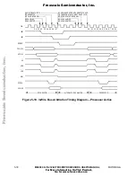
Страница 72: ... The assertion of the bus error signal during a bus cycle in which HALT is also asserted by an external device initiates a retry operation Figure 5 27 is a timing diagram of the retry operation The delayed BERR signal in the MC68010 also initiates a retry operation when HALT is asserted by an external device Figure 5 28 shows the timing of the delayed operation S0 S2 S4 S6 CLK FC2 FC0 A23 A1 S8 S0...

Страница 73: ...HALT is negated NOTE To guarantee that the entire read modify write cycle runs correctly and that the write portion of the operation is performed without negating the address strobe the processor does not retry a read modify write cycle When a bus error occurs during a read modify write operation a bus error operation is performed whether or not HALT is asserted 5 4 3 Halt Operation HALT HALT perf...

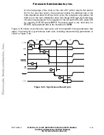
Страница 74: ...e halt operation and the hardware trace capability allow tracing of either bus cycles or instructions one at a time These capabilities and a software debugging package provide total debugging flexibility 5 4 4 Double Bus Fault When a bus error exception occurs the processor begins exception processing by stacking information on the supervisor stack If another bus error occurs during exception proc...

Страница 75: ...so clears the vector base register to 00000 No other register is affected by the reset sequence Figure 5 30 shows the timing of the reset operation T 4 CLOCKS 2 3 4 5 6 NOTES 1 Internal start up time 2 SSP high read in here 3 SSP low read in here 4 PC High read in here 5 PC Low read in here 6 First instruction fetched here Bus State Unknown All Control Signals Inactive Data Bus in Read Mode CLK 5 ...

Страница 76: ...sing edge of the processor clock The possible bus cycle termination can be summarized as follows case numbers refer to Table 5 5 Normal Termination DTACK is asserted BERR and HALT remain negated case 1 Halt Termination HALT is asserted coincident with or preceding DTACK and BERR remains negated case 2 Bus Error Termination BERR is asserted in lieu of coincident with or preceding DTACK case 3 In th...

Страница 77: ... etc A Signal asserted in this bus state NA Signal not asserted in this bus state X Don t care S Signal asserted in preceding bus state and remains asserted in this state NOTE All operations are subject to relevant setup and hold times The negation of BERR and HALT under several conditions is shown in Table 5 6 DTACK is assumed to be negated normally in all cases for reliable operation both DTACK ...

Страница 78: ...asynchronous manner Asynchronous bus operation uses the bus handshake signals to control the transfer of data The handshake signals are AS UDS LDS DS MC68008 only DTACK BERR HALT AVEC MC68EC000 only and VPA only for M6800 peripheral cycles AS indicates the start of the bus cycle and UDS LDS and DS signal valid data for a write cycle After placing the requested data on the data bus read cycle or la...

Страница 79: ...n by the processor clock is a common example of a pseudo asynchronous device The designer of a fully asynchronous system can make no assumptions about address setup time which could be used to improve performance With the system clock frequency known the slave device can be designed to decode the address bus before recognizing an address strobe Parameter 11 refer to Section 10 Electrical Character...

Страница 80: ...improve performance Parameter 29 is the minimum time a slave device can accept valid data before recognizing a data strobe The slave device asserts DTACK after it accepts the data Parameter 25 is the minimum time after negation of the strobes during which the valid data remains on the address bus Parameter 28 is the maximum time between the negation of the strobes by the processor and the negation...

Страница 81: ...e state of all bus signals relative to a specific state of the processor clock The standard M68000 bus cycle consists of four clock periods eight bus cycle states and optionally an integral number of clock cycles inserted as wait states Wait states are inserted as required to allow sufficient response time for the external device The following state by state description of the bus cycle differs fr...

Страница 82: ... by the processor If either DTACK or BERR is asserted before the falling edge of S4 and satisfies the input setup time defined by parameter 47 the processor enters S5 and the bus cycle continues If either DTACK or BERR is asserted but without meeting the setup time defined by parameter 47 the processor may recognize the signal and continue the bus cycle the result is unpredictable If neither DTACK...

Страница 83: ...o the negation of the AS and UDS LDS and or DS by negating DTACK and or BERR Parameter 28 is the hold time for DTACK and parameter 30 is the hold time for BERR Figure 5 35 shows a synchronous read cycle and the important timing parameters that apply The timing for a synchronous read cycle including relevant timing parameters is shown in Figure 5 36 ADDR UDS LDS R W AS CLOCK DTACK 6 9 S0 S1 S2 S3 S...

Страница 84: ...l synchronization requires that the internal machine receives a valid logic level not a metastable signal whether the input is high low or in transition Metastable signals propagating through synchronous machines can produce unpredictable operation Figure 5 37 is a conceptual representation of the input synchronizers used by the M68000 Family processors The input latches allow the input to propaga...

Страница 85: ...s the setup time required parameter 27 When parameter 27 has been met parameter 31 may be ignored If DTACK is asserted with the required setup time before the falling edge of S4 no wait states are incurred and the bus cycle runs at its maximum speed of four clock periods The late BERR in an MC68010 that is operating in a synchronous mode must meet setup time parameter 27A That is when BERR is asse...

Страница 86: ...ode Operation The exception processing state is associated with interrupts trap instructions tracing and other exceptional conditions The exception may be internally generated by an instruction or by an unusual condition arising during the execution of an instruction Externally exception processing can be forced by an interrupt by a bus error or by a reset Exception processing provides an efficien...

Страница 87: ...ome instructions having important system effects are designated privileged For example user programs are not permitted to execute the STOP instruction or the RESET instruction To ensure that a user program cannot enter the supervisor mode except in a controlled manner the instructions that modify the entire status register are privileged To aid in debugging systems software the move to user stack ...

Страница 88: ...ands in the supervisor mode perform the appropriate update to the status register and then fetch the next instruction at the next sequential program counter address in the privilege mode determined by the new S bit 6 1 4 Reference Classification When the processor makes a reference it classifies the reference according to the encoding of the three function code output lines This classification all...

Страница 89: ...ed internally or externally depending on the cause of the exception For interrupts during the interrupt acknowledge bus cycle a peripheral provides an 8 bit vector number see Figure 6 2 to the processor on data bus lines D7 D0 The processor forms the vector offset by left shifting the vector number two bit positions and zero filling the upper order bits to obtain a 32 bit long word vector offset I...

Страница 90: ...rocessors except the MC68008 this is 24 address bits A0 is implicitly encoded in the data strobes In the MC68008 the address is 20 or 22 bits in length The memory map for exception vectors is shown in Table 6 2 The vector table Table 6 2 is 512 words long 1024 bytes starting at address 0 decimal and proceeding through address 1023 decimal The vector table provides 255 unique vectors some of which ...

Страница 91: ...trap TRAP trap on overflow TRAPV check register against bounds CHK and divide DIV instructions can generate exceptions as part of their instruction execution In addition illegal instructions word fetches from odd addresses and privilege violations cause exceptions Tracing is similar to a very high priority internally generated interrupt following each instruction Freescale Semiconductor I Freescal...

Страница 92: ... Interrupt Autovector 1C 28 112 070 SD Level 4 Interrupt Autovector 1D 29 116 074 SD Level 5 Interrupt Autovector 1E 30 120 078 SD Level 6 Interrupt Autovector 1F 31 124 07C SD Level 7 Interrupt Autovector 20 2F 32 47 128 080 SD TRAP Instruction Vectors4 188 0BC 30 3F 48 631 192 0C0 SD Unassigned Reserved 255 0FF 40 FF 64 255 256 100 SD User Interrupt Vectors 1020 3FC NOTES 1 Vector numbers 12 13 ...

Страница 93: ...iolation Since only one instruction can be executed at a time no priority relationship applies within group 2 The priority relationship between two exceptions determines which is taken or taken first if the conditions for both arise simultaneously Therefore if a bus error occurs during a TRAP instruction the bus error takes precedence and the TRAP instruction processing is aborted In another examp...

Страница 94: ...ation The information stacked by a bus error or address error exception in the MC68000 MC68HC000 MC68HC001 MC68EC000 or MC68008 is described in 6 3 9 1 Bus Error and shown in Figure 6 7 The MC68000 MC68HC000 MC68HC001 MC68EC000 and MC68008 group 1 and 2 exception stack frame is shown in Figure 6 5 Only the program counter and status register are saved The program counter points to the next instruc...

Страница 95: ...6 5 Group 1 and 2 Exception Stack Frame MC68000 MC68HC000 MC68HC001 MC68EC000 and MC68008 PROGRAM COUNTER LOW PROGRAM COUNTER HIGH SP 0 15 STATUS REGISTER HIGHER ADDRESS VECTOR OFFSET FORMAT OTHER INFORMATION DEPENDING ON EXCEPTION Figure 6 6 MC68010 Stack Frame Freescale Semiconductor I Freescale Semiconductor Inc For More Information On This Product Go to www freescale com nc ...

Страница 96: ...ounter value usually points to the next unexecuted instruction However for bus error and address error the value stacked for the program counter is unpredictable and may be incremented from the address of the instruction that caused the error Group 1 and 2 exceptions use a short format exception stack frame format 0000 on the MC68010 Additional information defining the current context is stacked f...

Страница 97: ...ss than or equal to the current priority An interrupt request is made to the processor by encoding the interrupt request levels 1 7 on the three interrupt request lines all lines negated indicates no interrupt request Interrupt requests arriving at the processor do not force immediate exception processing but the requests are made pending Pending interrupts are detected between instruction executi...

Страница 98: ...onds by asserting DTACK or AVEC VPA BERR should be asserted to terminate the vector acquisition The processor separates the processing of this error from bus error by forming a short format exception stack and fetching the spurious interrupt vector instead of the bus error vector The processor then proceeds with the usual exception processing 6 3 5 Instruction Traps Traps are exceptions caused by ...

Страница 99: ...e bus cycle in which the function code lines FC2 FC0 are high and the address lines are all low is also executed before the stacking operations are performed The processor does not accept or send any data during this cycle Whether the breakpoint acknowledge cycle is terminated with a DTACK BERR or VPA signal the processor continues with the illegal instruction processing The purpose of this cycle ...

Страница 100: ...acing following each instruction When tracing is enabled an exception is forced after each instruction is executed Thus a debugging program can monitor the execution of the program under test The trace facility is controlled by the T bit in the supervisor portion of the status register If the T bit is cleared off tracing is disabled and instruction execution proceeds from instruction to instructio...

Страница 101: ...e copy of the status register are saved The value saved for the program counter is advanced 2 10 bytes beyond the address of the first word of the instruction that made the reference causing the bus error If the bus error occurred during the fetch of the next instruction the saved program counter has a value in the vicinity of the current instruction even if the current instruction is a branch a j...

Страница 102: ...eption 6 3 9 2 BUS ERROR MC68010 Exception processing for a bus error follows a slightly different sequence than the sequence for group 1 and 2 exceptions In addition to the four steps executed during exception processing for all other exceptions 22 words of additional information are placed on the stack This additional information describes the internal state of the processor at the time of the b...

Страница 103: ...ver enough information is placed on the stack for the bus error exception handler to determine why the bus fault occurred This additional information includes the address being accessed the function codes for the access whether it was a read or a write access and the internal register included in the transfer The fault address can be used by an operating system to determine what virtual memory loc...

Страница 104: ...be zero when written by the MC68010 Figure 6 9 Special Status Word Format 6 3 10 Address Error An address error exception occurs when the processor attempts to access a word or long word operand or an instruction at an odd address An address error is similar to an internally generated bus error The bus cycle is aborted and the processor ceases current processing and begins exception processing The...

Страница 105: ... read the remaining stack data checking for validity of the data The only word checked for validity is the first of the 16 internal information words SP 26 shown in Figure 5 8 This word contains a processor version number in bits 10 13 and proprietary internal information that must match the version number of the MC68010 attempting to read the data This validity check is used to ensure that the da...

Страница 106: ...ute the instruction Of the 18 clock periods 12 are used for the three read cycles four periods per cycle Four additional clock periods are used for the single write cycle for a total of 16 clock periods The bus is idle for two clock periods during which the processor completes the internal operations required for the instruction NOTE The total number of clock periods n includes instruction fetch a...

Страница 107: ...perand writes The total number of clock periods the number of read cycles and the number of write cycles are shown in the previously described format Table 7 2 Move Byte Instruction Execution Times Destination Source Dn An An An An d16 An d8 An Xn xxx W xxx L Dn An An 8 2 0 8 2 0 12 3 0 8 2 0 8 2 0 12 3 0 12 2 1 12 2 1 16 3 1 12 2 1 12 2 1 16 3 1 12 2 1 12 2 1 16 3 1 20 4 1 20 4 1 24 5 1 22 4 1 22...

Страница 108: ...4 24 2 4 24 2 4 40 6 4 32 4 4 32 4 4 48 8 4 34 4 4 34 4 4 50 8 4 32 4 4 32 4 4 48 8 4 40 6 4 40 6 4 56 10 4 An An d16 An 24 6 0 26 6 0 32 8 0 24 6 0 26 6 0 32 8 0 40 6 4 42 6 4 48 8 4 40 6 4 42 6 4 48 8 4 40 6 4 42 6 4 48 8 4 48 8 4 50 8 4 56 10 4 50 8 4 52 8 4 58 10 4 48 8 4 50 8 4 56 10 4 56 10 4 58 10 4 64 12 4 d8 An Xn xxx W xxx L 34 8 0 32 8 0 40 10 0 34 8 0 32 8 0 40 10 0 50 8 4 48 8 4 56 10...

Страница 109: ...fective address time The base time of 10 clock periods is increased to 12 if the effective address mode is register direct or immediate effective address time should also be added Only available effective address mode is data register direct DIVS DIVU The divide algorithm used by the MC68008 provides less than 10 difference between the best and worst case timings MULS MULU The multiply algorithm r...

Страница 110: ... Long 16 4 0 16 4 0 26 6 0 16 4 0 16 4 0 24 6 0 EORI Byte Word Long 16 4 0 16 4 0 28 6 0 20 4 1 24 4 2 40 6 4 MOVEQ Long 8 2 0 ORI Byte Word Long 16 4 0 16 4 0 28 6 0 20 4 1 24 4 2 40 6 4 SUBI Byte Word Long 16 4 0 16 4 0 28 6 0 12 2 1 16 2 2 24 2 4 SUBQ Byte Word Long 8 2 0 8 2 0 12 2 0 12 2 0 12 2 0 20 4 1 24 4 2 40 6 4 Add effective address calculation time 7 5 SINGLE OPERAND INSTRUCTION EXECUT...

Страница 111: ...and rotate instructions The total number of clock periods the number of read cycles and the number of write cycles are shown in the previously described format The number of clock periods the number of read cycles and the number of write cycles respectively must be added to those of the effective address calculation where indicated by a plus sign Table 7 8 Shift Rotate Instruction Execution Times ...

Страница 112: ... calculation time Indicates maximum value data addressing mode only 7 8 CONDITIONAL INSTRUCTION EXECUTION TIMES Table 7 10 lists the timing data for the conditional instructions The total number of clock periods the number of read cycles and the number of write cycles are shown in the previously described format The number of clock periods the number of read cycles and the number of write cycles r...

Страница 113: ... 0 32 8n 10 n 0 40 8n 10 2n 0 32 8n 8 2n 0 34 8n 8 2n 0 Long 24 16n 6 4n 0 24 16n 6 4n 0 32 16n 8 4n 0 34 16n 8 4n 0 32 16n 8 4n 0 40 16n 8 4n 0 32 16n 8 4n 0 34 16n 8 4n 0 MOVEM R M Word 16 8n 4 2n 16 8n 4 2n 24 8n 6 2n 26 8n 6 2n 24 8n 6 2n 32 8n 8 2n Long 16 16n 4 4n 16 16n 4 4n 24 16n 6 4n 26 16n 24 16n 8 4n 32 16n 6 4n n is the number of registers to move The size of the index register Xn doe...

Страница 114: ...7 11 MISCELLANEOUS INSTRUCTION EXECUTION TIMES Tables 7 13 and 7 14 list the timing data for miscellaneous instructions The total number of clock periods the number of read cycles and the number of write cycles are shown in the previously described format The number of clock periods the number of read cycles and the number of write cycles respectively must be added to those of the effective addres...

Страница 115: ... calculation time for word operand Table 7 14 Move Peripheral Instruction Execution Times Instruction Size Register Memory Memory Register MOVEP Word 24 4 2 24 6 0 Long 32 4 4 32 8 0 Add effective address calculation time 7 12 EXCEPTION PROCESSING EXECUTION TIMES Table 7 15 lists the timing data for exception processing The numbers of clock periods include the times for all stacking the vector fet...

Страница 116: ...Address Error 94 8 14 Bus Error 94 8 14 CHK Instruction 68 8 6 Divide by Zero 66 8 6 Interrupt 72 9 6 Illegal Instruction 62 8 6 Privilege Violation 62 8 6 RESET 64 12 0 Trace 62 8 6 TRAP Instruction 62 8 6 TRAPV Instruction 66 10 6 Add effective address calculation time Indicates the time from when RESET and HALT are first sampled as negated to when instruction execution starts Freescale Semicond...

Страница 117: ...ock periods is 18 Of the 18 clock periods 12 are used for the three read cycles four periods per cycle Four additional clock periods are used for the single write cycle for a total of 16 clock periods The bus is idle for two clock periods during which the processor completes the internal operations required for the instruction NOTE The total number of clock periods n includes instruction fetch and...

Страница 118: ...iods the number of read cycles and the number of write cycles are shown in the previously described format Table 8 2 Move Byte and Word Instruction Execution Times Destination Source Dn An An An An d16 An d8 An Xn xxx W xxx L Dn An An 4 1 0 4 1 0 8 2 0 4 1 0 4 1 0 8 2 0 8 1 1 8 1 1 12 2 1 8 1 1 8 1 1 12 2 1 8 1 1 8 1 1 12 2 1 12 2 1 12 2 1 16 3 1 14 2 1 14 2 1 18 3 1 12 2 1 12 2 1 16 3 1 16 3 1 16...

Страница 119: ...2 3 0 24 4 2 26 4 2 20 3 2 24 4 2 26 4 2 20 3 2 24 4 2 26 4 2 20 3 2 28 5 2 30 5 2 24 4 2 30 5 2 32 5 2 26 4 2 28 5 2 30 5 2 24 4 2 32 5 2 34 6 2 28 5 2 The size of the index register Xn does not affect execution time 8 3 STANDARD INSTRUCTION EXECUTION TIMES The numbers of clock periods shown in Table 8 4 indicate the times required to perform the operations store the results and read the next ins...

Страница 120: ...an 10 difference between the best and worst case timings MULS MULU The multiply algorithm requires 38 2n clocks where n is defined as MULU n the number of ones in the ea MULS n concatenate the ea with a zero as the LSB n is the resultant number of 10 or 01 patterns in the 17 bit source i e worst case happens when the source is 5555 8 4 IMMEDIATE INSTRUCTION EXECUTION TIMES The numbers of clock per...

Страница 121: ...yte Word 8 2 0 12 2 1 Long 16 3 0 20 3 2 SUBQ Byte Word 4 1 0 8 1 0 8 1 1 Long 8 1 0 8 1 0 12 1 2 8 5 SINGLE OPERAND INSTRUCTION EXECUTION TIMES Table 8 6 lists the timing data for the single operand instructions The total number of clock periods the number of read cycles and the number of write cycles are shown in the previously described format The number of clock periods the number of read cycl...

Страница 122: ...tructions The total number of clock periods the number of read cycles and the number of write cycles are shown in the previously described format The number of clock periods the number of read cycles and the number of write cycles respectively must be added to those of the effective address calculation where indicated by a plus sign Table 8 7 Shift Rotate Instruction Execution Times Instruction Si...

Страница 123: ... BCLR Byte 8 1 1 12 2 1 Long 10 1 0 14 2 0 BSET Byte 8 1 1 12 2 1 Long 8 1 0 12 2 0 BTST Byte 4 1 0 8 2 0 Long 6 1 0 10 2 0 Add effective address calculation time Indicates maximum value data addressing mode only 8 8 CONDITIONAL INSTRUCTION EXECUTION TIMES Table 8 9 lists the timing data for the conditional instructions The total number of clock periods the number of read cycles and the number of ...

Страница 124: ...18 4n 4 n 0 16 4n 4 n 0 20 4n 5 n 0 16 4n 4n 0 18 4n 4 n 0 Long 12 8n 3 2n 0 12 8n 3 n 0 16 8n 4 2n 0 18 8n 4 2n 0 16 8n 4 2n 0 20 8n 5 2n 0 16 8n 4 2n 0 18 8n 4 2n 0 MOVEM R M Word 8 4n 2 n 8 4n 2 n 12 4n 3 n 14 4n 3 n 12 4n 3 n 16 4n 4 n Long 8 8n 2 2n 8 8n 2 2n 12 8n 3 2n 14 8n 3 2n 12 8n 3 2n 16 8n 4 2n n is the number of registers to move The size of the index register Xn does not affect the ...

Страница 125: ...STRUCTION EXECUTION TIMES Tables 8 12 and 8 13 list the timing data for miscellaneous instructions The total number of clock periods the number of read cycles and the number of write cycles are shown in the previously described format The number of clock periods the number of read cycles and the number of write cycles respectively must be added to those of the effective address calculation where i...

Страница 126: ... MOVE to USP 4 1 0 NOP 4 1 0 RESET 132 1 0 RTE 20 5 0 RTR 20 2 0 RTS 16 4 0 STOP 4 0 0 SWAP 4 1 0 TRAPV 4 1 0 UNLK 12 3 0 Add effective address calculation time Table 8 13 Move Peripheral Instruction Execution Times Instruction Size Register Memory Memory Register MOVEP Word 16 2 2 16 4 0 Long 24 2 4 24 6 0 8 12 EXCEPTION PROCESSING EXECUTION TIMES Table 8 14 lists the timing data for exception pr...

Страница 127: ...xception Processing Execution Times Exception Periods Address Error 50 4 7 Bus Error 50 4 7 CHK Instruction 40 4 3 Divide by Zero 38 4 3 Illegal Instruction 34 4 3 Interrupt 44 5 3 Privilege Violation 34 4 3 RESET 40 6 0 Trace 34 4 3 TRAP Instruction 34 4 3 TRAPV Instruction 34 5 3 Add effective address calculation time The interrupt acknowledge cycle is assumed to take four clock periods Indicate...

Страница 128: ...where n is the total number of clock periods r is the number of read cycles w is the number of write cycles For example a timing number shown as 18 3 1 means that 18 clock cycles are required to execute the instruction Of the 18 clock periods 12 are used for the three read cycles four periods per cycle Four additional clock periods are used for the single write cycle for a total of 16 clock period...

Страница 129: ... 8 2 0 8 2 0 2 0 0 4 0 0 An d16 An Address Register Indirect with Predecrement Address Register Indirect with Displacement 6 1 0 8 2 0 4 0 0 4 0 0 10 2 0 12 3 0 4 0 0 4 1 0 d8 An Xn xxx W Address Register Indirect with Index Absolute Short 10 2 0 8 2 0 8 1 0 4 1 0 14 3 0 12 3 0 8 1 0 4 1 0 xxx L d16 PC Absolute Long Program Counter Indirect with Displacement 12 3 0 8 2 0 8 2 0 16 4 0 12 3 0 8 2 0 ...

Страница 130: ...5 1 22 4 1 20 4 1 24 5 1 26 5 1 24 5 1 28 6 1 d16 PC d8 PC Xn data 12 3 0 14 3 0 8 2 0 12 3 0 14 3 0 8 2 0 16 3 1 18 3 1 12 2 1 16 3 1 18 3 1 12 2 1 16 3 1 18 3 1 12 2 1 20 4 1 22 4 1 16 3 1 22 4 1 24 4 1 18 3 1 20 4 1 22 4 1 16 3 1 24 5 1 26 5 1 20 4 1 The size of the index register Xn does not affect execution time Table 9 3 Move Byte and Word Instruction Loop Mode Execution Times Loop Continued...

Страница 131: ...tion Loop Mode Execution Times Loop Continued Loop Terminated Valid Count cc False Valid count cc True Expired Count Destination Source An An An An An An An An An Dn An An 14 0 2 14 0 2 22 2 2 14 0 2 14 0 2 22 2 2 24 2 2 20 2 2 20 2 2 28 4 2 20 2 2 20 2 2 28 4 2 30 4 2 18 2 2 18 2 2 24 4 2 18 2 2 18 2 2 24 4 2 26 4 2 An An 22 2 2 24 2 2 22 2 2 24 2 2 24 2 2 26 2 2 28 4 2 30 4 2 28 4 2 30 4 2 30 4 ...

Страница 132: ...unt Instruction Size op ea An op ea Dn op Dn ea op ea An op ea Dn op Dn ea op ea An op ea Dn op Dn ea ADD Byte Word 18 1 0 16 1 0 16 1 1 24 3 0 22 3 0 22 3 1 22 3 0 20 3 0 20 3 1 Long 22 2 0 22 2 0 24 2 2 28 4 0 28 4 0 30 4 2 26 4 0 26 4 0 28 4 2 AND Byte Word 16 1 0 16 1 1 22 3 0 22 3 1 20 3 0 20 3 1 Long 22 2 0 24 2 2 28 4 0 30 4 2 26 4 0 28 4 2 CMP Byte Word 12 1 0 12 1 0 18 3 0 18 3 0 16 3 0 1...

Страница 133: ...ord 8 2 0 12 2 1 Long 14 3 0 20 3 2 ADDQ Byte Word 4 1 0 4 1 0 8 1 2 Long 8 1 0 8 1 1 12 1 2 ANDI Byte Word 8 2 0 12 2 1 Long 14 3 0 20 3 1 CMPI Byte Word 8 2 0 8 2 0 Long 12 3 0 12 3 0 EORI Byte Word 8 2 0 12 2 1 Long 14 3 0 20 3 2 MOVEQ Long 4 1 0 ORI Byte Word 8 2 0 12 2 1 Long 14 3 0 20 3 2 SUBI Byte Word 8 2 0 12 2 1 Long 14 3 0 20 3 2 SUBQ Byte Word 4 1 0 4 1 0 8 1 1 Long 8 1 0 8 1 0 12 1 2 ...

Страница 134: ...S Byte 4 1 0 14 2 1 TST Byte Word 4 1 0 4 1 0 Long 4 1 0 4 1 0 Add effective address calculation time Use nonfetching effective address calculation time Table 9 10 Clear Instruction Execution Times Size Dn An An An An d16 An d8 An Xn xxx W xxx L CLR Byte Word 4 1 0 8 1 1 8 1 1 10 1 1 12 2 1 16 2 1 12 2 1 16 3 1 Long 6 1 0 12 1 2 12 1 2 14 1 2 16 2 2 20 2 2 16 2 2 20 3 2 The size of the index regis...

Страница 135: ... 28 4 2 28 4 2 30 4 2 TST Byte Word 12 1 0 12 1 0 14 1 0 18 3 0 18 3 0 20 3 0 16 3 0 16 3 0 18 3 0 Long 18 2 0 18 2 0 20 2 0 24 4 0 24 4 0 26 4 0 20 4 0 20 4 0 22 4 0 9 6 SHIFT ROTATE INSTRUCTION EXECUTION TIMES Tables 9 12 and 9 13 list the timing data for the shift and rotate instructions The total number of clock periods the number of read cycles and the number of write cycles are shown in the ...

Страница 136: ... are shown in the previously described format The number of clock periods the number of read cycles and the number of write cycles respectively must be added to those of the effective address calculation where indicated by a plus sign Table 9 14 Bit Manipulation Instruction Execution Times Dynamic Static Instruction Size Register Memory Register Memory BCHG Byte 8 1 1 12 2 1 Long 8 1 0 12 2 0 BCLR...

Страница 137: ... 0 12 3 0 8 2 0 12 2 0 PEA 12 1 2 16 2 2 20 2 2 16 2 2 20 3 2 16 2 2 20 2 2 MOVEM M R Word 12 4n 3 n 0 12 4n 3 n 0 16 4n 4 n 0 18 4n 4 n 0 16 4n 4 n 0 20 4n 5 n 0 16 4n 4 n 0 18 4n 4 n 0 Long 24 8n 3 2n 0 12 8n 3 2n 0 16 8n 4 2n 0 18 8n 4 2n 0 16 8n 4 2n 0 20 8n 5 2n 0 16 8n 4 2n 0 18 8n 4 2n 0 MOVEM R M Word 8 4n 2 n 8 4n 2 n 12 4n 3 n 14 4n 3 n 12 4n 3 n 16 4n 4 n Long 8 8n 2 2n 8 8n 2 2n 12 8n ...

Страница 138: ...4 0 Long 20 5 0 24 4 0 30 6 0 26 6 0 SUBX Byte Word 4 1 18 3 1 22 2 1 28 4 1 26 4 1 Long 6 1 0 30 5 2 32 4 2 38 6 2 36 6 2 ABCD Byte 6 1 0 18 3 1 24 2 1 30 4 1 28 4 1 SBCD Byte 6 1 0 18 3 1 24 2 1 30 4 1 28 4 1 Source and destination ea are An for CMPM and An for all others 9 11 MISCELLANEOUS INSTRUCTION EXECUTION TIMES Table 9 18 lists the timing data for miscellaneous instructions The total numb...

Страница 139: ...0 MOVE to USP 6 1 0 MOVEC 10 2 0 12 2 0 MOVEP Word 16 2 2 16 4 0 Long 24 2 4 24 6 0 NOP 4 1 0 ORI to CCR 16 2 0 ORI to SR 16 2 0 RESET 130 1 0 RTD 16 4 0 RTE Short 24 6 0 Long Retry Read 112 27 10 Long Retry Write 112 26 1 Long No Retry 110 26 0 RTR 20 5 0 RTS 16 4 0 STOP 4 0 0 SWAP 4 1 0 TRAPV 4 1 0 UNLK 12 3 0 Add effective address calculation time Use nonfetching effective address calculation t...

Страница 140: ...cated by a plus sign Table 9 19 Exception Processing Execution Times Exception Address Error 126 4 26 Breakpoint Instruction 45 5 4 Bus Error 126 4 26 CHK Instruction 44 5 4 Divide By Zero 42 5 4 Illegal Instruction 38 5 4 Interrupt 46 5 4 MOVEC Illegal Control Register 46 5 4 Privilege Violation 38 5 4 Reset 40 6 0 RTE Illegal Format 50 7 4 RTE Illegal Revision 70 12 4 Trace 38 4 4 TRAP Instructi...

Страница 141: ...rmation on the maximum rating and thermal characteristics for the MC68000 MC68HC000 MC68HC001 MC68EC000 MC68008 and MC68010 10 1 MAXIMUM RATINGS Rating Symbol Value Unit Supply Voltage VCC 0 3 to 7 0 V Input Voltage Vin 0 3 to 7 0 V Maximum Operating Temperature Range Commerical Extended C Grade Commerical Extended I Grade TA TL to TH 0 to 70 40 to 85 0 to 85 C Storage Temperature Tstg 55 to 150 C...

Страница 142: ...wer dissipation of 1 5 W over the ambient temperature range of 55 C to 125 C using a maximum θ JA of 45 C W Ambient temperature is that of the still air surrounding the device Lower values of θJA cause the curve to shift downward slightly for instance for θJA of 40 W the curve is just below 1 4 W at 25 C The total thermal resistance of a package θJA can be separated into two components θJC and θCA...

Страница 143: ...the power dissipation curve shown in Figure 10 1 is negatively sloped power dissipation declines as ambient temperature increases Therefore maximum power dissipation occurs at the lowest rated ambient temperature but the highest average junction temperature occurs at the maximum ambient temperature where power dissipation is lowest POWER P WATTS D AMBIENT TEMPERATURE T C A 2 2 2 0 1 8 1 6 1 4 1 2 ...

Страница 144: ...0 C 40 1 5 38 1 2 101 NOTE Table does not include values for the MC68000 12F Does not apply to the MC68HC000 MC68HC001 and MC68EC000 Values for thermal resistance presented in this manual unless estimated were derived using the procedure described in Motorola Reliability Report 7843 Thermal Resistance Measurement Method for MC68XXX Microcomponent Devices and are provided for design purposes only T...

Страница 145: ...input output drive requirements of CMOS logic devices 2 The HCMOS MC68HC000 and MC68EC000 provides an order of magnitude reduction in power dissipation when compared to the HMOS MC68000 However the MC68HC000 does not offer a power down mode 10 5 AC ELECTRICAL SPECIFICATION DEFINITIONS The AC specifications presented consist of output delays input setup and hold times and signal skew times All sign...

Страница 146: ...ll parameters specified relative to the rising edge of the clock 3 This timing is applicable to all parameters specified relative to the negation of the RESET signal LEGEND A Maximum output delay specification B Minimum output hold time C Minimum input setup time specification D Minimum input hold time specification E Mode select setup time to RESET negated F Mode select hold time from RESET negat...

Страница 147: ... µA E IOH 400 µA AS A1 A23 BG D0 D15 FC0 FC2 LDS R W UDS VMA VOH VCC 0 75 2 4 2 4 V Output Low Voltage IOL 1 6 mA HALT IOL 3 2 mA A1 A23 BG FC0 FC2 IOL 5 0 mA RESET IOL 5 3 mA E AS D0 D15 LDS R W UDS VMA VOL 0 5 0 5 0 5 0 5 V Power Dissipation see POWER CONSIDERATIONS PD W Capacitance Vin 0 V TA 25 C Frequency 1 MHz Cin 20 0 pF Load Capacitance HALT All Others CL 70 130 pF With external pullup res...

Страница 148: ... Frequency 1 MHz Cin 20 0 pF Load Capacitance HALT All Others CL 70 130 pF Current listed are with no loading Capacitance is periodically sampled rather than 100 tested 10 8 AC ELECTRICAL SPECIFICATIONS CLOCK TIMING See Figure 10 3 Applies To All Processors Except The MC68EC000 Num Characteristic 8 MHz 10 MHz 12 5 MHz 16 67 MHz 12F 16 MHz 20 MHZ Unit Min Max Min Max Min Max Min Max Min Max Min Max...

Страница 149: ...er previously published specifications for the 8 and 10 MHz MC68008 and are valid only for product bearing date codes of 8827 and later 0 8 V 2 0 V Timing measurements are referenced to and from a low voltage of 0 8 V and a high voltage of 2 0 V unless otherwise noted The voltage swing through this range should start outside and pass through the range such that the rise or fall will be linear betw...

Страница 150: ... 30 45 40 ns 121 Clock Low to AS DS Negated 62 50 40 40 3 30 3 25 ns 132 AS DS Negated to Address FC Invalid 40 30 20 10 15 10 ns 142 ASand DS Read Width Asserted 270 195 160 120 120 100 ns 14A DS Width Asserted Write 140 95 80 60 60 50 ns 152 AS DS Width Negated 150 105 65 60 60 50 ns 16 Clock High to Control Bus High Impedance 80 70 60 50 50 42 ns 172 AS DS Negated to R W Invalid 40 30 20 10 15 ...

Страница 151: ...sserted 62 50 40 40 0 30 0 25 ns 34 Clock High to BG Negated 62 50 40 40 0 30 0 25 ns 35 BR Asserted to BG Asserted 1 5 3 5 1 5 3 5 1 5 3 5 1 5 3 5 1 5 3 5 1 5 3 5 Clks 367 BR Negated toBG Negated 1 5 3 5 1 5 3 5 1 5 3 5 1 5 3 5 1 5 3 5 1 5 3 5 Clks 37 BGACK Asserted to BG Negated 1 5 3 5 1 5 3 5 1 5 3 5 1 5 3 5 1 5 3 5 1 5 3 5 Clks 37A8 BGACK Asserted to BR Negated 20 1 5 Clks 20 1 5 Clks 20 1 5 ...

Страница 152: ...columns 2 Actual value depends on clock period 3 If 47 is satisfied for both DTACK and BERR 48 may be ignored In the absence of DTACK BERR is an asynchronous input using the asynchronous input setup time 47 4 For power up the MC68000 must be held in the reset state for 100 ms to allow stabilization of on chip circuitry After the system is powered up 56 refers to the minimum pulse width required to...

Страница 153: ...ge of the clock 2 BR need fall at this time only to insure being recognized at the end of the bus cycle 3 Timing measurements are referenced to and from a low voltage of 0 8 V and a high voltage of 2 0 V unless otherwise noted The voltage swing through this range should start outside and pass through the range such that the rise or fall is linear between 0 8 V and 2 0 V 9 15 29A Figure 10 4 Read C...

Страница 154: ...f 2 0 V unless otherwise noted The voltage swing through this range should start outside and pass through the range such that the rise or fall is linear between 0 8 V and 2 0 V 2 Because of loading variations R W may be valid after AS even though both are initiated by the rising edge of S2 specification 20A 23 21A 7 11 11A 9 14A 53 7 55 21 22 20A 20 Figure 10 5 Write Cycle Timing Diagram Applies T...

Страница 155: ...20 0 90 0 70 0 50 0 50 0 42 ns 45 E Low to Control Address Bus Invalid Address Hold Time 30 10 10 10 10 10 ns 47 Asynchronous Input Setup Time 10 10 10 10 10 5 ns 492 AS DS Negated to E Low 70 70 55 55 45 45 35 35 35 35 30 30 ns 50 E Width High 450 350 280 220 220 190 ns 51 E Width Low 700 550 440 340 340 290 ns 54 E Low to Data Out Invalid 30 20 15 10 10 5 ns These specifications represent improv...

Страница 156: ...or those who wish to design their own circuit to generate VMA It shows the best case possible attainable 23 18 41 20 42 51 47 40 43 50 42 41 12 49 18 44 45 41 54 29 27 45 Figure 10 6 MC68000 to M6800 Peripheral Timing Diagram Best Case Applies To All Processors Except The MC68EC000 Freescale Semiconductor I Freescale Semiconductor Inc For More Information On This Product Go to www freescale com nc...

Страница 157: ...etup Time 10 10 10 5 5 5 ns 57 BGACK Negated to AS DS R W Driven 1 5 1 5 1 5 1 5 1 5 1 5 Clks 57A BGACK Negated to FC VMA Driven 1 1 1 1 1 1 Clks 581 BR Negated to AS DS R W Driven 1 5 1 5 1 5 1 5 1 5 1 5 Clks 58A1 BR Negated to FC VMA Driven 1 1 1 1 1 1 Clks These specifications represent improvement over previously published specifications for the 8 10 and 12 5 MHz MC68000 and are valid only for...

Страница 158: ...onous inputs BERR BGACK BR DTACK IPL2 IPL0 and VPA guarantees their recognition at the next falling edge of the clock BR BGACK BG AND R W STROBES Figure 10 7 Bus Arbitration Timing Applies To All Processors Except The MC68EC000 Freescale Semiconductor I Freescale Semiconductor Inc For More Information On This Product Go to www freescale com nc ...

Страница 159: ...A0 D7 D0 NOTES Waveform measurements for all inputs and outputs are specified at logic high 2 0 V logic low 0 8 V 1 MC68008 52 Pin Version only 1 Figure 10 8 Bus Arbitration Timing Applies To All Processors Except The MC68EC000 Freescale Semiconductor I Freescale Semiconductor Inc For More Information On This Product Go to www freescale com nc ...

Страница 160: ...0 NOTES Waveform measurements for all inputs and outputs are specified at logic high 2 0 V logic low 0 8 V 1 MC68008 52 Pin Version only 1 Figure 10 9 Bus Arbitration Timing Idle Bus Case Applies To All Processors Except The MC68EC000 Freescale Semiconductor I Freescale Semiconductor Inc For More Information On This Product Go to www freescale com nc ...

Страница 161: ...NOTE Waveform measurements for all inputs and outputs are specified at logic high 2 0 V logic low 0 8 V 1 MC68008 52 Pin Version Only 7 1 Figure 10 10 Bus Arbitration Timing Active Bus Case Applies To All Processors Except The MC68EC000 Freescale Semiconductor I Freescale Semiconductor Inc For More Information On This Product Go to www freescale com nc ...

Страница 162: ...OTES Waveform measurements for all inputs and outputs are specified at logic high 2 0 V logic low 0 8 V 1 MC68008 52 Pin Version only 1 Figure 10 11 Bus Arbitration Timing Multiple Bus Request Applies To All Processors Except The MC68EC000 Freescale Semiconductor I Freescale Semiconductor Inc For More Information On This Product Go to www freescale com nc ...

Страница 163: ...OH 400 µA FC2 FC0 LDS R W UDS VOH VCC 0 75 V Output Low Voltage IOL 1 6 mA HALT IOL 3 2 mA A23 A0 BG FC2 FC0 IOL 5 0 mA RESET IOL 5 3 mA AS D15 D0 LDS R W UDS VOL 0 5 0 5 0 5 0 5 V Current Dissipation f 8 MHz f 10 MHz f 12 5 MHz f 16 67 MHz f 20 MHz ID 25 30 35 50 70 mA Power Dissipation f 8 MHz f 10 MHz f 12 5 MHz f 16 67 MHz f 20 MHz PD 0 13 0 16 0 19 0 26 0 38 W Capacitance Vin 0 V TA 25 C Freq...

Страница 164: ... Width Asserted 270 195 160 120 100 ns 14A2 DS Width Asserted Write 140 95 80 60 50 ns 152 AS DS Width Negated 150 105 65 60 50 ns 16 Clock High to Control Bus High Impedance 55 55 55 50 42 ns 172 AS DS Negated to R W Invalid 15 15 15 15 10 ns 181 Clock High to R W High Read 0 35 0 35 0 35 0 30 0 25 ns 201 Clock High to R W Low Write 0 35 0 35 0 35 0 30 0 25 ns 20A2 6 AS Asserted to R W Low Write ...

Страница 165: ... 0 ns 564 HALT RESET Pulse Width 10 10 10 10 10 Clks 587 BR Negated to AS DS R W Driven 1 5 1 5 1 5 1 5 1 5 Clks 58A7 BR Negated to FC VMA Driven 1 1 1 1 1 Clks NOTES 1 For a loading capacitance of less than or equal to 50 pF subtract 5 ns from the value given in the maximum columns 2 Actual value depends on clock period 3 I f 47 is satisfied for both DTACK and BERR 48 may be ignored In the absenc...

Страница 166: ... the next falling edge of the clock 2 BR need fall at this time only to insure being recognized at the end of the bus cycle 3 Timing measurements are referenced to and from a low voltage of 0 8 V and a high voltage of 2 0 V unless otherwise noted The voltage swing through this range should start outside and pass through the range such that the rise or fall is linear between 0 8 V and 2 0 V 9 15 Fi...

Страница 167: ...d a high voltage of 2 0 V unless otherwise noted The voltage swing through this range should start outside and pass through the range such that the rise or fall is linear between 0 8 V and 2 0 V 2 Because of loading variations R W may be valid after AS even though both are initiated by the rising edge of S2 specification 20A 23 21A 7 11 11A 9 14A 53 7 55 21 22 20A 20 Figure 10 13 MC68EC000 Write C...

Страница 168: ... Asserted to BG Asserted 1 5 3 5 1 5 3 5 1 5 3 5 1 5 3 5 1 5 3 5 Clks 367 BR Negated to BG Negated 1 5 3 5 1 5 3 5 1 5 3 5 1 5 3 5 1 5 3 5 Clks 38 BG Asserted to Control Address Data Bus High Impedance AS Negated 55 55 55 50 42 ns 39 BG Width Negated 1 5 1 5 1 5 1 5 1 5 Clks 47 Asynchronous Input Setup Time 5 5 5 5 5 ns 581 BR Negated to AS DS R W Driven 1 5 1 5 1 5 1 5 1 5 Clks 58A1 BR Negated to...

Страница 169: ...W FC2 FC0 A19 A0 D7 D0 NOTES Waveform measurements for all inputs and outputs are specified at logic high 2 0 V logic low 0 8 V 38 39 Figure 10 14 MC68EC000 Bus Arbitration Timing Diagram Freescale Semiconductor I Freescale Semiconductor Inc For More Information On This Product Go to www freescale com nc ...

Страница 170: ...ge dimensions for the devices described in this manual 11 1 PIN ASSIGNMENTS Package 68000 68008 68010 68HC000 68HC001 68EC000 64 Pin Dual In Line 68 Terminal Pin Grid Array 64 Lead Quad Pack 68 Lead Quad Flat Pack 52 Lead Quad 48 Pin Dual In Line Freescale Semiconductor I Freescale Semiconductor Inc For More Information On This Product Go to www freescale com nc ...

Страница 171: ...R VCC GND HALT RESET VMA E VPA BERR IPL2 IPL0 IPL1 FC2 FC1 FC0 A1 A2 A3 A4 1 2 3 4 5 6 7 8 9 10 11 12 13 14 15 16 17 18 19 20 21 22 23 24 25 26 27 28 29 30 31 32 64 63 62 61 60 59 58 57 56 55 54 53 52 51 50 49 48 46 47 45 44 43 42 41 40 39 38 37 36 35 34 33 MC68000 MC68010 MC68HC000 Figure 11 1 64 Pin Dual In Line Freescale Semiconductor I Freescale Semiconductor Inc For More Information On This P...

Страница 172: ...5 6 7 8 9 10 A B C D E F G H J K LDS MC68000 MC68010 MC68HC000 MODE E VMA HALT CLK BR BGACK DTACK NC FC2 RESET GND VCC BG AS FC0 FC1 R W UDS D1 A1 NC D0 D2 A3 A2 A4 A5 A6 A8 A7 A10 A13 D3 D4 D6 D5 D9 D7 D11 D8 D13 A9 A11 A12 A15 A18 VCC GND A23 D14 D10 NC A14 A16 A17 A19 A20 A21 A22 D15 D12 BERR IPL0 IPL2 IPL1 VPA BOTTOM VIEW 1 2 3 4 5 6 7 8 9 10 A B C D E F G H J K LDS MC68HC001 Figure 11 2 68 Le...

Страница 173: ...10 18 26 27 44 43 35 9 68 60 52 61 MC68000 MC68HC000 MC68010 GND A18 A17 A16 A15 A14 A13 A12 VCC D13 D14 D15 A19 A21 A23 A22 D5 D6 D7 D4 D3 D2 D1 D0 AS R W LDS UDS D8 D9 D10 D11 D12 A0 A11 A10 A9 A8 A7 A6 A5 FC2 FC1 FC0 A1 A2 A3 A4 IPL0 CLK NC DTACK BG BR HALT RESET AVEC BERR IPL1 VCC GND GND IPL2 BGACK MODE 1 10 18 26 27 44 43 35 9 68 60 52 61 MC68EC000 GND A20 GND Figure 11 3 68 Lead Quad Pack 1...

Страница 174: ...C GND GND IPL2 VMA BGACK MODE 1 10 18 26 27 44 43 35 9 68 60 52 61 MC68HC001 Figure 11 3 68 Lead Quad Pack 2 of 2 CLK E GND FC0 FC1 FC2 A0 A1 A2 A3 A4 A5 A8 A7 A6 IPL0 A18 A9 A10 A12 GND A16 A13 CC V A14 A17 A11 A15 1 8 20 21 34 33 7 52 46 47 D0 D1 D2 D3 D4 D5 D6 A19 A20 D7 R W DS AS BGACK BG DTACK BR HALT RESET VPA BERR IPL1 IPL2 MC68008 21 A Figure 11 4 52 Lead Quad Pack Freescale Semiconductor ...

Страница 175: ... D6 D5 D4 D3 1 2 3 4 5 6 7 8 9 10 11 12 13 14 15 16 17 18 19 20 21 22 23 24 48 47 46 45 44 43 42 41 40 39 38 37 36 35 34 33 32 30 31 29 28 27 26 25 A2 A15 RESET HALT AS DS R W DTACK BG BR VPA BERR IPL1 IPL2 IPL0 MC68008 Figure 11 5 48 Pin Dual In Line Freescale Semiconductor I Freescale Semiconductor Inc For More Information On This Product Go to www freescale com nc ...

Страница 176: ...CC MODE GND IPL2 AVEC 1 16 17 33 32 64 48 49 IPL0 FC2 GND MC68EC000 Figure 11 6 64 Lead Quad Flat Pack 11 2 PACKAGE DIMENSIONS Case Package 68000 68008 68010 68HC000 68HC001 68EC000 740 03 L Suffix 767 02 P Suffix 746 01 LC Suffix 754 01 R and P Suffix 765A 05 RC Suffix 778 02 FN Suffix 779 02 FN Suffix 779 01 FN Suffix 847 01 FC Suffix 840B 01 FU Suffix Freescale Semiconductor I Freescale Semicon...

Страница 177: ... Y14 5m 1982 DIM MILLIMETERS INCHES MIN MAX MIN MAX A B C D F G J K L M N 60 36 61 56 2 376 2 424 14 64 15 34 0 576 0 604 3 05 4 32 0 120 0 160 3 81 0 533 0 015 0 021 762 1 397 0 030 0 055 2 54 BSC 0 100 BSC 0 204 0 330 0 008 0 013 2 54 4 19 0 100 0 165 0 10 0 10 1 016 1 524 0 040 0 060 33 A T M 0 25 0 010 T A M 15 24 BSC 0 600 BSC Figure 11 7 Case 740 03 L Suffix Freescale Semiconductor I Freesca...

Страница 178: ...NG PER ANSI Y14 5 1982 6 CONTROLLING DIMENSION INCH DIM MILLIMETERS INCHES MIN MAX MIN MAX A B C D F G H J K L M N 61 34 62 10 2 415 2 445 13 72 14 22 0 540 0 560 3 94 5 08 0 155 0 200 0 36 0 55 0 014 0 022 1 02 1 52 0 040 0 060 2 54 BSC 0 100 BSC 0 20 0 38 0 008 0 015 2 92 3 81 0 115 0 135 15 24 BSC 0 600 BSC 0 15 0 15 0 51 1 02 0 020 0 040 1 79 BSC 0 070 BSC 25 R T M 0 51 0 020 T B R POSITIONAL ...

Страница 179: ...SI Y14 5 1973 DIM MILLIMETERS INCHES MIN MAX MIN MAX A B C D F G J K L M N 80 52 82 04 3 170 3 230 22 25 22 96 0 876 0 904 3 05 4 32 0 120 0 160 0 38 0 53 0 015 0 021 76 1 40 0 030 0 055 2 54 BSC 0 100 BSC 0 20 0 33 0 008 0 013 2 54 4 19 0 100 0 165 22 61 0 890 0 10 0 10 1 02 1 52 0 040 0 060 33 A T 23 11 0 910 M 0 25 0 010 T A M Figure 11 9 Case 746 01 LC Suffix Freescale Semiconductor I Freescal...

Страница 180: ...NG PER ANSI Y14 5 1982 DIM MILLIMETERS INCHES MIN MAX MIN MAX A B C D F G J K L M N 81 16 81 91 3 195 3 225 20 17 20 57 0 790 0 810 4 83 5 84 0 190 0 230 0 33 0 53 0 013 0 021 1 27 1 77 0 050 0 070 2 54 BSC 0 100 BSC 0 20 0 38 0 008 0 015 3 05 3 55 0 120 0 140 22 86 BSC 0 9 00 BSC 0 15 0 15 0 51 1 02 0 020 0 040 33 T 2 T IS SEATING PLANE M 0 25 0 010 T A M M B Figure 11 10 Case 754 01 R and P Suff...

Страница 181: ...8000 8 16 32 BIT MICROPROCESSORS USER S MANUAL MOTOROLA Figure 11 11 Case 765A 05 RC Suffix Freescale Semiconductor I Freescale Semiconductor Inc For More Information On This Product Go to www freescale com nc ...

Страница 182: ... added to the value in the program counter and the instruction at the resulting address is executed Figure A 1 shows the source code of a program fragment containing a loop that executes in the loop mode in the MC68010 The program moves a block of data at address SOURCE to a block starting at address DEST The number of words in the block is labeled LENGTH If any word in the block at address SOURCE...

Страница 183: ...r fetches the looped instruction the second time and determines that the looped instruction is a loop mode instruction the processor automatically enters the loop mode and no more instruction fetches occur until the count is exhausted or the loop condition is true In addition to the normal termination conditions for the loop several abnormal conditions cause the MC68010 to exit the loop mode These...

Страница 184: ... Ay to Dx ADDA WL CMPA WL SUBA WL Ay to Ax Ay to Ax Ay to Ax ADD BWL AND BWL EOR BWL OR BWL SUB BWL Dx to Ay Dx to Ay Dx to Ay ABCD B ADDX BWL SBCD B SUBX BWL Ay to Ax CMP BWL Ay to Ax CLR BWL NEG BWL NEGX BWL NOT BWL TST BWL NBCD B Ay Ay Ay ASL W ASR W LSL W LSR W ROL W ROR W ROXL W ROXR Ay by 1 Ay by 1 Ay by 1 NOTE B W or L indicate an operand size of byte word or long word Freescale Semiconduct...

Страница 185: ......

Страница 186: ......

Страница 187: ......

Страница 188: ......

Страница 189: ......

Отзывы: