MOTOROLA
DSP96002 USER’S MANUAL
7 - 9
machine is responsible for ensuring that
—
R
—
A
–
S or
—
C
—
A
–
S timeouts do not occur. Since typical
—
R
—
A
–
S and
—
C
—
A
–
S timeouts are 10-100
µ
sec, one of the simplest solutions is to perform a hardware refresh
which deasserts both
—
R
—
A
–
S and
—
C
—
A
–
S. If refresh is performed often enough,
—
R
—
A
–
S and
—
C
—
A
–
S timeout will never happen.
The serial port of VRAM devices is clocked by a serial clock SC. Since the serial shift register is dynamic,
there is a minimum frequency at which the shift register must be clocked to refresh its contents. This fre-
quency is typically about 20 kHz (50
µ
sec refresh period). The DSP96002 does not provide any internal sup-
port for SC timeouts. The external state machine is responsible for ensuring that SC timeouts do not occur.
If an SC timeout does occur, the external state machine cancels (ignores) the effect of the
—
T
–
T signal in
the next external bus cycle to force a reload of the serial shift register. Fortunately, future 1Mbit VRAMs are
being specified with static shift registers so the SC timeout problem should go away.
7.2.2.4
DMA Accesses
External DMA accesses to P, X or Y memory spaces are normal bus cycles and cannot be distinguished
from CPU read/write cycles. Therefore DMA accesses can use the
—
T
–
T pin and do not need any special
treatment by external hardware.
7.2.2.5
Multiple Memory Banks
Multiple memory banks exist when there are more external memories than needed just to cover the 32-bit
data bus size. In this case, the external memory controller typically selects between banks by enabling one
of several row address strobe (
—
R
—
A
–
S) signals or column address strobe (
—
C
—
A
–
S) signals based on
several address lines. Since changes from one memory bank to another will cause a page fault, multiple
memory banks are allowed and no special treatment is required.
7.2.2.6
Multiple Memory Controllers
Multiple memory controllers may exist to support fast access modes with multiple external physical memo-
ries. Since the page circuit can monitor multiple memory spaces and detect or ignore changes in memory
spaces, multiple memory controllers are allowed and no special treatment is required.
7.3
EXPANSION PORTS SELECTION
Every memory space (X, Y and P) is divided into 8 equal portions. The division is fixed, that is, the sizes of
the portions are fixed at 0.5 gigawords per portion and the address boundaries are fixed. Each portion of
each memory space may be individually assigned to one of the external expansion ports (Port A or B). The
mapping is controlled by the Port Select Register (PSR).
7.3.1 Port Select Register (PSR)
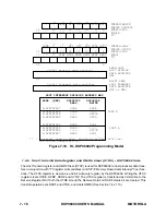
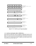
The Port Select Register is a 32-bit wide read/write register situated in the X I/O memory space. For each
portion of each memory space there is a bit in the Port Select Register (PSR): if the bit is cleared, the re-
spective portion goes thorough Port A, and if the bit is set, then it goes thorough Port B. Any memory seg-
Содержание DSP96002
Страница 3: ...1 2 DSP96002 USER S MANUAL MOTOROLA ...
Страница 38: ...MOTOROLA DSP96002 USER S MANUAL 3 15 Figure 3 4 Modulo Arithmetic Unit Block Diagram ...
Страница 39: ...3 16 DSP96002 USER S MANUAL MOTOROLA ...
Страница 53: ...4 14 DSP96002 USER S MANUAL MOTOROLA ...
Страница 76: ...MOTOROLA DSP96002 USER S MANUAL 5 23 Figure 5 8 Address Modifier Summary ...
Страница 86: ...6 10 DSP96002 USER S MANUAL MOTOROLA ...
Страница 101: ...MOTOROLA DSP96002 USER S MANUAL 7 15 Figure 7 9 HI Block Diagram One Port ...
Страница 140: ...7 54 DSP96002 USER S MANUAL MOTOROLA ...
Страница 166: ...9 10 DSP96002 USER S MANUAL MOTOROLA ...
Страница 181: ...MOTOROLA DSP96002 USER S MANUAL 10 15 Figure 10 8 Program Address Bus FIFO ...
Страница 336: ...A 148 DSP96002 USER S MANUAL MOTOROLA FMPY S2 S1 D1 FSUB S S3 D2 move syntax see the MOVE instruction de scription ...
Страница 337: ...MOTOROLA DSP96002 USER S MANUAL A 149 ...
Страница 404: ...A 216 DSP96002 USER S MANUAL MOTOROLA PC xxxx D ...
Страница 460: ...A 272 DSP96002 USER S MANUAL MOTOROLA SIOP Not affected ...
Страница 484: ...A 296 DSP96002 USER S MANUAL MOTOROLA SSH PC SSL SR SP 1 SP ...
Страница 519: ...MOTOROLA DSP96002 USER S MANUAL A 331 ...
Страница 580: ...MOTOROLA DSP96002 USER S MANUAL B 61 X Memory Y Memory n0 3 r0 x0 Xmin r4 y0 Xmax z0 Ymin x1 Ymax y1 Zmin z1 Zmax ...
Страница 718: ...MOTOROLA DSP96002 USER S MANUAL B 199 ...
Страница 871: ... MOTOROLA INC 1994 MOTOROLA TECHNICAL DATA SEMICONDUCTOR M Addendum ...
Страница 888: ...MOTOROLA INDEX 1 INDEX ...
Страница 889: ......

