


7 - 34
DSP96002 USER’S MANUAL
MOTOROLA
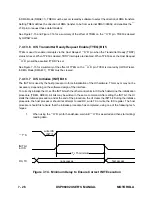
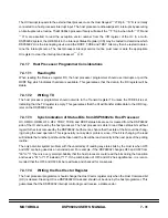
where this pin is defined as a DMA service request input. When
—
H
–
R is asserted, the master DMA Con-
troller transfers the data word from the external address that selects the RX register in the slave’s HI to a
master memory location. After RX is read (negating
—
H
–
R), the HI may transfer the next data word from
the HI HTX register, setting HTDE and RXDF. Setting RXDF causes
—
H
–
R to be asserted if RREQ is set.
In the slave’s DMA Controller, HTDE is defined as a DMA service request signal. When HTDE is asserted,
the slave’s DMA Controller initiates a data transfer from the slave memory to the HTX register, keeping the
register full for further data transfers.
7.4.20
External DMA Controller to DSP96002 Data Transfers - Examples
This section presents examples showing the use of the HI and the on-chip DMA Controller for data transfers
between a DSP96002 and an external DMA Controller. The external DMA Controller is the bus master and
the DSP96002 is the bus slave. The external DMA Controller accesses the DSP96002 HI without supplying
an address to select a HI register. Note that the HI is programmed to work in the DMA Mode (DMAE=1).
7.4.20.1
Data Write Using the DSP96002 On-Chip DMA Controller
This example outlines the steps that an external DMA Controller, the bus master, takes to transfer data to
a DSP96002 bus slave, thorough the slave’s HI. The on-chip DMA Controller of the DSP96002 is used to
locally transfer data between the HI and the DSP96002 memory without interfering with core processing.
The TREQ and RREQ bits in the ICS register must be programmed to define the direction of data transfer
as being from the external DMA Controller to the HI (TREQ=1, RREQ=0). The TYEQ bit in the ICS register
DSP96002 Bus Master
DMA Destination
DSP96002 Bus Slave
DMA Source
DMA Request
Bus Master
Read Bus Cycle
into Memory
—
I
—
R
–
Q
S1, S0
A0–A31
—
T
–
A
—
T
–
S
R/
—
W
space
address
data
V
cc
full
slave
select
decode
—
H
–
R
—
H
–
S
—
H
–
A
A2–A5
—
T
–
S
R/
—
W
D0–D31
DMA Request
Memory
→
Host
DMA Transfer
Host Data Empty
Figure 7-18. DSP96002 to DSP96002 Data Read
Receive Data Full
(RXDF=1)
(HTDE=1)
Содержание DSP96002
Страница 3: ...1 2 DSP96002 USER S MANUAL MOTOROLA ...
Страница 38: ...MOTOROLA DSP96002 USER S MANUAL 3 15 Figure 3 4 Modulo Arithmetic Unit Block Diagram ...
Страница 39: ...3 16 DSP96002 USER S MANUAL MOTOROLA ...
Страница 53: ...4 14 DSP96002 USER S MANUAL MOTOROLA ...
Страница 76: ...MOTOROLA DSP96002 USER S MANUAL 5 23 Figure 5 8 Address Modifier Summary ...
Страница 86: ...6 10 DSP96002 USER S MANUAL MOTOROLA ...
Страница 101: ...MOTOROLA DSP96002 USER S MANUAL 7 15 Figure 7 9 HI Block Diagram One Port ...
Страница 140: ...7 54 DSP96002 USER S MANUAL MOTOROLA ...
Страница 166: ...9 10 DSP96002 USER S MANUAL MOTOROLA ...
Страница 181: ...MOTOROLA DSP96002 USER S MANUAL 10 15 Figure 10 8 Program Address Bus FIFO ...
Страница 336: ...A 148 DSP96002 USER S MANUAL MOTOROLA FMPY S2 S1 D1 FSUB S S3 D2 move syntax see the MOVE instruction de scription ...
Страница 337: ...MOTOROLA DSP96002 USER S MANUAL A 149 ...
Страница 404: ...A 216 DSP96002 USER S MANUAL MOTOROLA PC xxxx D ...
Страница 460: ...A 272 DSP96002 USER S MANUAL MOTOROLA SIOP Not affected ...
Страница 484: ...A 296 DSP96002 USER S MANUAL MOTOROLA SSH PC SSL SR SP 1 SP ...
Страница 519: ...MOTOROLA DSP96002 USER S MANUAL A 331 ...
Страница 580: ...MOTOROLA DSP96002 USER S MANUAL B 61 X Memory Y Memory n0 3 r0 x0 Xmin r4 y0 Xmax z0 Ymin x1 Ymax y1 Zmin z1 Zmax ...
Страница 718: ...MOTOROLA DSP96002 USER S MANUAL B 199 ...
Страница 871: ... MOTOROLA INC 1994 MOTOROLA TECHNICAL DATA SEMICONDUCTOR M Addendum ...
Страница 888: ...MOTOROLA INDEX 1 INDEX ...
Страница 889: ......


