background image


10 - 4

DSP96002 USER’S MANUAL

MOTOROLA

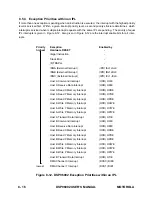
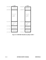
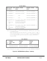
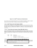
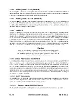
Figure 10-2.  OnCE


 Controller and Serial Interface 


been received), and two signals indicating that the core was halted and the DMA was halted. The ODEC

generates all the strobes required for reading and writing the selected OnCE


 registers. 


 10.3.4

OnCE


 Status and Control Register (OSCR) 


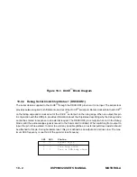
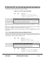
The Status and Control Register is a 32-bit register used to select the events that will put the chip in Debug

Mode (see Figure 10-3). Breakpoints may be disabled or enabled on one or more memory spaces. The

Trace Mode of operation is also selected from OSCR. The control bits are read/write while the status bits

are read only.


 10.3.4.1 Program Memory Breakpoint Enable (PBE0-PBE1) Bits 0-1 


These control bits unmask program memory breakpoints allowing break-point interrupts to occur when a

program memory address is within the low and high program memory address registers and will select

whether the breakpoint will be recognized for read or write accesses. These bits are cleared on hardware

reset. 


 PBE1    PBE0    Selection


     0       0      Breakpoint disabled
     0       1      Breakpoint on write accesses
     1       0      Breakpoint on read  accesses
     1       1      Breakpoint on both read and write accesses


 10.3.4.2 Program Memory Breakpoint Selection (PBS0-PBS1) Bits 2-3 


These control bits select whether the program memory breakpoints will be recognized on core program

memory fetches, core program memory accesses (MOVEM or MOVEP) or DMA program memory access-

es. These bits are cleared on hardware reset. 

Содержание DSP96002

Страница 1: ...DSP96002 32 BIT DIGITAL SIGNAL PROCESSOR USER S MANUAL Motorola Inc Semiconductor Products Sector DSP Division 6501 William Cannon Drive West Austin Texas 78735 8598 ...

Страница 2: ...int and 32 bit signed and unsigned fixed point arithmetic coupled with two identical external memory expansion ports Its features are listed below DSP96002 Features IEEE 745 Standard SP 32 bit and SEP 44 bit Arithmetic 16 5 Million Instructions per Second Mips with a 33 Mhz clock 49 5 Million Floating Point Instructions per Second MFLOPS peak with a 33 Mhz clock Single Cycle 32 x 32 Bit Parallel M...

Страница 3: ...1 2 DSP96002 USER S MANUAL MOTOROLA ...

Страница 4: ...ging to reliably reset the chip If R E S E T is deas serted synchronous to the input clock CLK exact startup timing is guaranteed allow ing multiple processors to startup synchronously and operate together in lock step When the R E S E T pin is deasserted the initial chip operating mode is latched from the MODA MODB and MODC pins MODA I R Q A Mode Select A External Interrupt Request A active low i...

Страница 5: ... Data and Address 152 Bus Control 44 TOTALS 223 Figure 2 1 DSP96002 Functional Group Pin Allocation MODB I R Q B Mode Select B External Interrupt Request B active low input internally synchronized to the input clock CLK MODB I R Q B selects the initial chip operating mode dur ing hardware reset and becomes a level sensitive or negative edge triggered maskable interrupt request input during normal ...

Страница 6: ... S a B L b B L a T T b T T a T S b T S a T A b T A a A E b A E a D E b D E a H S b H S a H A b H A a H R b H R a B R b B R a B G b B G a B B b B B a B A b B A aNC 2 2 bNC V cc 1 1 V cc V ss 2 2 V ss INTERRUPT AND OnCE ON CHIP MODE CONTROL EMULATION PORT MODA I R Q A DSO MODB I R Q B DSI OS0 MODC I R Q C DSCK OS1 R E S E T D R CLOCK INPUT NOISY POWER PLANE CLK 2 V cc NC 5 V ss QUIET POWER QUIET POW...

Страница 7: ...ed by pairing a t2 and tw phase CLK should be continuous with a 46 54 duty cycle Quiet VCC 4 Power isolated power for the CPU logic Must be tied to all other chip power pins ex ternally User must provide adequate external decoupling capacitors Quiet VSS 4 Ground isolated ground for the CPU logic Must be tied to all other chip ground pins externally User must provide adequate external decoupling ca...

Страница 8: ...nly when the DSP 96002 has entered the debug mode of operation When configured as an output not in Debug Mode this pin in conjunction with the OS1 pin provides information about the chip status DSO Debug Serial Output The debug serial output provides the data contained in one of the OnCE controller registers as specified by the last command received from the external command controller When a trac...

Страница 9: ...stated during hardware reset These signals can be viewed in different ways depending on how the external memo ries are mapped They support the trend toward splitting memory spaces among ports and mapping multiple memory spaces into the same physical memory locations Sev eral examples are given in Figure 2 3 The encoding S1 S0 11 may be used to place external memories in their low power standby mod...

Страница 10: ...uring an instruction cycle or a fault is detected by the page circuit during an external access T T remains deasserted The parameters of the page circuit fault detection are user programmable T T is three stated during hardware reset T S Transfer Strobe three state active low output when a bus master active low input when not a bus master When a bus master T S is asserted to indicate that the ad d...

Страница 11: ...input clock CLK Any number of wait states 0 1 2 infinity may be inserted by keeping T A deasserted In typical operation T A is deasserted at the start of a bus cycle is asserted to enable completion of the bus cycle and is deasserted before the next bus cycle The current bus cycle completes one clock period after T A is asserted synchronous to CLK The number of wait states is determined by the T A...

Страница 12: ...utput drivers are three stated regardless of whether D E is asserted or deasserted Read only bus cycles may be performed even though D E is deasserted The function of D E is to allow multiplexed bus systems to be implemented Examples are a multi plexed address data bus such as the NuBus used in the Macintosh II or a multi plexed data1 data2 bus used for long word transfers with one 32 bit wide mem...

Страница 13: ...ng bus mastership B R is deasserted when the CPU or DMA no longer needs the bus B R may be asserted or deasserted independent of whether the DSP96002 is a bus master or a bus slave Bus parking allows B R to be deasserted even though the DSP96002 is the bus master See the description of bus parking in the B A pin description The RH bit in the Bus Control Register see Section seven allows B R to be ...

Страница 14: ... gardless of whether B R is asserted or deasserted This is called bus parking and allows the current bus master to use the bus repeatedly without re arbitration until some other device wants the bus The current bus master keeps B A asserted during indivisible read modify write bus cycles regardless of whether B G has been deasserted by the external bus arbitra tion unit This form of bus locking al...

Страница 15: ...ernal ports are designed to interface with a wide variety of memory and peripheral devices high speed static RAMs dynamic RAMs and video RAMs as well as slower memory devices External bus timing is controlled by the T A control signal and by the Bus Con trol Registers BCR which are described in Section seven The BCR and T A control the timing of the bus interface signals Insertion of wait states i...

Страница 16: ...the data is latched in the destination device At the end of a read cycle the DSP96002 latches the data inter nally At the end of a write cycle the external memory latches the data The Address signals remain stable until the first phase of the next external bus cycle to minimize power dissipa tion The Memory Reference signals S1 and S0 are deasserted during periods of no bus ac tivity and the data ...

Страница 17: ...e disadvantage of this technique is that the write data hold will be shortened because the W E signal is delayed by the OR gate 3 6 2 Dynamic RAM and Video RAM Support Modern dynamic memory DRAM and video memory VRAM are becoming the preferred choice for a wide variety of computing systems based on 4 7 Cost per bit due to dynamic storage cell density 4 8 Packaging density due to multiplexed addres...

Страница 18: ...rbitration signal The local arbitration signals run between a potential bus master and the arbitration logic The local signals are B R B G and B A B B is a system arbitration signal These signals are described below B R Bus Request Asserted by the requesting device to indicate that it wants to use the bus and is held asserted until it no longer needs the bus This includes time when it is the bus m...

Страница 19: ... DSP96002 bus master releases its ownership deasserts B A after completing the current external bus access If an instruction is executing a Read Modify Write external access a DSP96002 master asserts the B L signal and will only relinquish the bus and deassert B L after completing the entire Read Modify Write sequence When the current bus master deasserts B A the B B signal must also be deasserted...

Страница 20: ... 2 Bus Handshake Unit The bus handshake unit in the DSP96002 is implemented within a finite state machine It consists of two external outputs B R B A two external inputs B G B B and three internal inputs ext_acc_req end_of_sequence RH see Figure 2 8 The ext_acc_req signal is asserted when one or more requests for external bus access are pending and remains asserted as long as the transfers are bei...

Страница 21: ...nd destination states The equa tions of the transition arcs are described as follows XX ext_acc_req B G B B XY ext_acc_req B G B B XZ ext_acc_req B G B B XW ext_acc_req B G B B YX ext_acc_req B G B B note 1 YY ext_acc_req B G B B YZ ext_acc_req B G B B YW ext_acc_req B G B B note 1 ZX ext_acc_req B G ZY ext_acc_req D B G end_of_sequence note 3 ACTIVE_ MASTER Z B R 0 B A 0 Figure 2 9 Bus Handshake ...

Страница 22: ...al If the device requesting mastership asserts B R the arbiter asserts the requesting devices B G and B B is deasserted indicating the bus is not busy The requesting device will assert B A 5 16 3 2 Case 2 Bus Busy If the device requesting mastership asserts B R the arbiter responds by asserting the requesting devic es B G however the bus is busy because B B is asserted The requesting device will n...

Страница 23: ...master at a time That is referring to Figure 2 10 B L can be input from DSP 1to the memory controller which prevents T A from being asserted by the controller thereby suspending the memory access by DSP 2 until DSP 1 completes its RMW access 5 16 3 6 Case 6 Bus Park The device requesting mastership asserts B R the arbiter asserts the requesting devices B G and B B is deasserted indicating the bus ...

Страница 24: ...ogram Memory Port A and Port B External Bus Interfaces Internal Bus Switch and Bit Manipulation Unit I O Interfaces An overall block diagram of the DSP96002 architecture is shown in Figure 3 1 3 2 1 Data Buses Data movement on the chip occurs over five bidirectional 32 bit buses X Data Bus XDB Y Data Bus YDB Global Data Bus GDB the DMA Data Bus DDB and the Program Data Bus PDB The X and Y data bus...

Страница 25: ...ia a single 32 bit unidirectional address bus driven by a three input multiplexer that can select the X Address Bus XAB the Y Address Bus YAB or the Program Address Bus PAB On chip peripherals and the DMA Controller are memory mapped in the internal X memory space When zero wait state external memory is used one instruction cycle is needed for each external memory access The XAB YAB and PAB are du...

Страница 26: ...Flush to Zero mode is also provided which forces all floating point result underflows to zero all denormalized input operands are considered as being zero The Flush to Zero mode never requires any additional instruction cycles Refer to Section 3 3 for a detailed description of the Data ALU architecture 3 2 4 AGU The AGU performs all of the address storage and effective address calculations necessa...

Страница 27: ...on entering this state the current instruction in decode will execute normally unless it is the first word of a two word instruction in which case it will be aborted and re fetched at the completion of exception processing The next two fetch addresses are supplied by the interrupt controller During these fetches the PC is not updated If one of the words fetched by the interrupt controller is a jum...

Страница 28: ...aces Each bus interface has a 32 bit wide address bus and a 32 bit wide data bus and may be used to access external Data Memory Program Memory or I O devices Separate select lines control access to the memory spaces A Port Select control register permits assigning sections of each memory space to each external bus interface port Refer to Section 2 and Sec tion 9 for a detailed description of the e...

Страница 29: ...sing modes are linear bit reversed and modulo For more details see Section 7 5 3 3 DATA ALU BLOCK DIAGRAM The major components of the Data ALU are Data ALU Register File Multiply Unit Adder Unit Logic Unit Format Converter Divide and Square Root Unit Controller and Arbitrator A block diagram of the Data ALU architecture is shown in Figure 3 2 D0 D1 D2 D3 D4 D5 D6 D7 D8 and D9 are 96 bit registers ...

Страница 30: ...ers Dn L is used as source and or destination for most integer operations In this case the integer registers supply an operand for the Multiplier and the Adder Subtracter while receiving an input from the Multiplier and the Adder subtracter Note that in the case of integer multiplication the result will be 64 bits wide and will be stored in both middle and low portions of the destination register ...

Страница 31: ...rounding to IEEE single precision is specified explicitly by the instruction or implicitly by the MR register the result is rounded to 24 bit mantissa accord ing to IEEE Standard 754 for single precision The four IEEE rounding modes are supported the rounding mode is specified by the rounding mode bits R1 R0 in the IER register 3 3 1 2 Multiplier Control Recoder The multiplier control decoder dire...

Страница 32: ...The Subtract Unit performs automatic rounding to 32 bit result mantissa for the floating point add subtract according to the IEEE Stan dard for single extended precision arithmetic If rounding to IEEE single precision is specified the result is rounded to 24 bit mantissa according to the IEEE Standard for single precision arithmetic The type of rounding is specified by the rounding mode bits in th...

Страница 33: ...red by the processing units of the Data ALU and register file and is responsible for the full implementation of the IEEE standard For the latter task the actions taken by the controller and arbitrator are determined by the FZ bit in the SR register In the Flush to Zero mode all denormalized input operands are considered as being zero and all denormalized results are flushed to zero Denormalized nu...

Страница 34: ...ning if an address register R is the destination of a MOVE instruction the new contents will not be available for use as a pointer until the second following instruction 3 4 2 Offset Register Files Each of two Offset Register Files consists of four 32 bit registers The two files contain the offset registers N0 N3 and N4 N7 respectively and usually hold offset values used to update address pointers...

Страница 35: ...a modifier register M is the destination of a MOVE instruction the new contents will not be available for use in address calculations until the second following instruction 3 4 4 Temporary Address Registers There are two kinds of temporary registers in the AGU TempR high and low and TempN high and low The temporary address registers TempR Low and TempR High are 32 bit registers which provide tempo...

Страница 36: ...address register file or temporary register Each modulo arithmetic unit can update one address register Rn from its respective address register file during one instruction cycle It is capable of performing linear reverse carry and modulo arithmetic The contents of the selected modifier register specifies the type of arithmetic to be used in an address register update calculation The modifier value...

Страница 37: ...OROLA address output multiplexers are shared by the DMA and the AGU The output multiplexers are time multi plexed the first half instruction cycle is assigned to DMA transfers while the second half cycle is assigned to core transfers ...

Страница 38: ...MOTOROLA DSP96002 USER S MANUAL 3 15 Figure 3 4 Modulo Arithmetic Unit Block Diagram ...

Страница 39: ...3 16 DSP96002 USER S MANUAL MOTOROLA ...

Страница 40: ... flexible control of these parallel processing re sources Many instructions allow the programmer to keep each unit busy thus enhancing program execu tion speed The programming model is shown in Figure 4 1 and Figure 4 2 and is described in the following sections Program Controller Reserved bits always read as zero should be written with zero for future compatibil ity Figure 4 1 DSP96002 Programmin...

Страница 41: ...2 bit registers or as ten 96 bit floating point registers Each 96 bit register is divided into three sub registers high middle and low Each sub registers may be addressed individually by specifying the register number and the name of the sub registers e g D0 H D0 M D0 L The low sub register is used as source and destination for the integer operations When writing to or reading from a sub register ...

Страница 42: ... register is used in the calculation of the effective address of an operand This address may point to data directly or may be modified by a register offset Most addressing modes modify the selected address register in a read modify write fashion Typically the address register is accessed used as input to its associated modulo arithmetic unit modified by the arithmetic unit and writ ten back into t...

Страница 43: ... the user writing the IER register The purpose of making bits sticky is to prevent them from accidentally being cleared before being processed or used later by other instructions The standard definition of the IER bits and the complete IER exception flag computa tion rules are given in Section A 5 It is strongly recommended that users of the DSP96002 obtain and com prehend the ANSI IEEE Standard 7...

Страница 44: ...IEEE Inexact IEEE Divide by Zero IEEE Underflow IEEE Overflow IEEE Invalid Operation Rounding Mode Reserved IER Figure 4 3 SR Format UN S OP CC NAN NAN ERR OVF UNF DZ INX 15 14 13 12 11 10 9 8 Inexact Divide by Zero Underflow Overflow Operand error Signaling NaN Not A Number Unordered Condition ER A R LR I N Z V C 7 6 5 4 3 2 1 0 Carry Overflow Zero Negative Infinity Local Reject Reject Accept CCR...

Страница 45: ...finity bit is set if the result of a floating point operation is infinity The I bit is not affected by fixed point operations The I bit is cleared during processor reset 4 7 6 CCR Local Reject LR Bit 5 The local reject bit is used for trivial reject testing of floating point or fixed point operands in graphics appli cations The LR bit is cleared during processor reset 4 7 7 CCR Reject R Bit 6 The ...

Страница 46: ...umber with round to minus infinity also re turns 7F7FFFFF but sets OVF see Section C 1 5 1 General for additional information on the rounding modes The OVF bit is not affected by fixed point operations The OVF bit is cleared during processor re set 4 7 13 ER Operand Error OPERR Bit 12 The operand error bit is set if an operation has no mathematical interpretation for the given operands Examples of...

Страница 47: ...ocessor reset 4 7 19 IER IEEE Underflow Flag SUNF Bit 18 The IEEE underflow flag is the IEEE flag for trap disabled operations and is set when both tininess UNF is set and loss of accuracy INX is set have been detected i e the INX bit and the UNF bit were set simul taneously in the current or a previous instruction The SUNF flag is cleared during processor reset 4 7 20 IER IEEE Overflow Flag SOVF ...

Страница 48: ...d for future expansion and will read as zero during read operations They should be written with zero for future compatibility 4 7 24 MR Multiply Precision Control MP Bit 26 The multiply precision control bit specifies the output precision of the multiply operation in the FMPY FADD FMPY FADDSUB and FMPY FSUB instructions If MP is cleared then the output precision of the multiply operation is determ...

Страница 49: ...hich detects the end of a program loop The loop flag is the only SR bit which is restored when terminating a program loop Stack ing and restoring the loop flag when initiating and exiting a program loop respectively allow the nesting of program loops The loop flag is cleared during a processor reset 4 8 LOOP COUNTER LC The loop counter is a special 32 bit counter used to specify the number of time...

Страница 50: ... as well as the SR LA and LC register contents just prior to the start of the loop This allows nesting of DO loops Up to 15 long interrupts 7 DO loops or 15 JSRs or combinations of these can be accommodated by the Stack Care must be taken when approaching the stack limit When the Stack limit is exceeded the data to be stacked will be lost and a non maskable Stack Error interrupt will occur 4 11 ST...

Страница 51: ...the second move should be to from the SSH to automatically trigger a SP increment decrement 4 11 2 Stack Error flag SE Bit 4 The Stack Error flag SE indicates that a stack error has occurred The transition of SE from 0 to 1 causes the priority level 3 Stack Error exception see Section 8 When the stack is completely full the Stack Pointer reads 001111 and any operation that pushes data to the stack...

Страница 52: ...structions which directly reference the OMR The operating mode register format is shown in Figure 4 6 and is described below 4 12 1 Chip Operating Mode Bits 0 1 2 The operating mode bits MA MB and MC determine if the internal program RAM is enabled and the startup procedure when the chip leaves the RESET state These bits are loaded from the external Mode Select pins MODC MODB and MODA respectively...

Страница 53: ...4 14 DSP96002 USER S MANUAL MOTOROLA ...

Страница 54: ...eger 32 bits wide with two s complement representation Signed Long Word Integer 64 bits wide with two s complement representation Unsigned Word Integer 32 bits wide with unsigned magnitude representation Unsigned Long Word Integer 64 bits wide with unsigned magnitude representation The bit weighting for signed integers is presented in Figure 5 1 The bit weighting for unsigned integers is presented...

Страница 55: ... LONG WORD INTEGER 2 0 21 262 263 SIGNED WORD INTEGER 2 0 21 230 231 31 30 1 0 SIGNED LONG WORD INTEGER 2 0 21 262 263 63 62 1 0 Figure 5 1 Bit Weighting and Alignment of Signed Integer Operands 31 30 1 0 63 62 1 0 Figure 5 2 Bit Weighting and Alignment of Unsigned Integer Operands ...

Страница 56: ... 5 2 2 1 IEEE Single Precision Real Memory Format Summary 23 Bit Fraction 11 Bit Exponent S 52 Bit Fraction 8 Bit Exponent S SINGLE REAL DOUBLE REAL Sign of Significand Sign of Significand Figure 5 3 Memory Format for floating point Operands 31 30 23 22 0 63 62 52 51 0 Field Size in bits s Sign 1 e Biased Exponent 8 f Fraction 23 Interpretation of Sign Positive Mantissa s 0 Negative Mantissa s 1 N...

Страница 57: ...s Represents real infinities in the form 1 s x 2 Emax 1 127 x 1 0 Bias of e 127 7F e 255 FF f Zero Mantissa 1 f 1 00 00 NaNs Not a Number Represents NaNs as 2 Emax 1 127 x 1 f s Don t care Bias of e n a e 255 FF f Non Zero 11 11 Internal legal QNaN 1x xx recognized QNaN 0x xx SNaN 5 2 2 2 Double Precision Real Memory Format Summary Fraction S Biased Exponent 63 62 52 51 0 63 0 Field Size in bits s...

Страница 58: ...0 00 Signed Infinities Represents infinities in the form 1 s x 2 Emax 1 1023 x 1 0 Bias of e n a e 2047 7FF f Zero Mantissa 1 f 1 00 00 NaNs Not a Number Represents NaNs as 2 Emax 1 1023 x 1 f s Don t care Bias of e n a e 2047 7FF f Non Zero 11 11 Internal legal QNaN 1x xx Recognized QNaN 0x xx SNaN 5 3 DATA ORGANIZATION IN REGISTERS 5 3 1 Data ALU Registers The thirty Data ALU registers are 32 bi...

Страница 59: ... Zero Zero I U V 95 94 93 92 75 74 64 11 10 Figure 5 4 Data Format in the Floating Point Registers When a result of an internal operations which is a single extended precision number in the DSP96002 is written into a Data ALU register or when writing single or double precision numbers represented in one of the memory data formats to a Data ALU register as a result of a MOVE operation automatic for...

Страница 60: ...gative Mantissa s 1 Normalized Numbers Represents real numbers in the form 1 s x 2 e 1023 x 1 f Bias of e 1023 3FF e 0 e 2047 7FF i 1 f Zero or Non Zero Mantissa i f 1 f Denormalized Numbers Represents real numbers in the form 1 s x 2 1022 x 0 f Bias of e 1022 3FE e 0 000 i 0 f Non Zero Mantissa i f 0 f Signed Zeros Bias of e n a e 0 000 i 0 f Zero Mantissa i f 0 00 00 Signed Infinities Bias of e ...

Страница 61: ...code register CCR occupying the low order 8 bits The SR register may be accessed as a word operand The MR IER ER and CCR registers may be accessed as byte operands The loop counter register LC loop address register LA system stack pointer SP system stack high SSH and system stack low SSL are 32 bits wide and may be accessed as word operands The program counter register PC is a special 32 bit wide ...

Страница 62: ...rnal floating point operands are converted to double precision values before writing them into a Data ALU floating point register The conversion is actually a bit rearranging operation using the procedure shown in Figure 5 5 When converting a single precision number to the internal register data format the implicit bit is revealed and stored as an explicit bit in the register If the number to be c...

Страница 63: ...ARED IF ZERO INV BIT 30 OTHERWISE 71 SET IF NAN OR INFINITY CLEARED IF ZERO INV BIT 30 OTHERWISE 29 70 23 64 63 I CLEARED IF DENORM OR ZERO SET OTHERWISE 22 62 0 40 39 CLEARED 0 CLEARED Double Precision Double Precision Memory Format Internal Format 63 95 S 94 U CLEARED 93 V SET IF DENORMALIZED CLEARED OTHERWISE 92 CLEARED 75 CLEARED 62 74 52 64 63 I CLEARED IF DENORM OR ZERO SET OTHERWISE 51 62 0...

Страница 64: ... Zero mode the result will be stored as zero in the register In the IEEE mode the operand will be first corrected by adding to the execution cycle extra cycles for denormalization However the data stored in the register will be in the internal double precision format and the U tag will be set The U tag indicates that if another Data ALU operation will use this result as an operand extra cycles sho...

Страница 65: ... Double Precision Internal Format Memory Format 95 63 94 75 74 62 64 52 63 62 51 11 0 10 0 Figure 5 6 Conversion from Internal Format to Memory Formats 5 6 3 R Register References Register references called R references are references to the Data ALU Address Generation Unit and Program Controller registers Data may be read from one register and written into another register ...

Страница 66: ...and one word operand is in Y memory space 5 6 4 4 1 Two independent addresses Two independent addresses are used to access two word operands Two effective addresses in the in struction are used to derive two independent operand addresses one operand address may reference X memory space or Y memory space and the other operand address must reference the other memory space One of the two effective ad...

Страница 67: ...gister Rn having the same register number n Thus the assigned registers are M0 N0 R0 M1 N1 R1 M2 N2 R2 M3 N3 R3 M4 N4 R4 M5 N5 R5 M6 N6 R6 and M7 N7 R7 The address register Rn is used as the address register the offset register Nn is used to specify an optional offset and the modifier register Mn is used to specify an addressing mode modifier The addressing modes are grouped into three categories ...

Страница 68: ...d address is used it is decre mented by 1 and stored in the same address register The type of arithmetic used to increment Rn is de termined by Mn The Nn register is ignored This reference is classified as a memory reference 5 7 2 4 Postincrement by Offset Nn Rn Nn The address of the operand is in the address register Rn After the operand address is used it is incre mented added by the contents of...

Страница 69: ...elative addressing modes the address of the operand is obtained by adding a displacement represented in two s complement format to the value of the program counter PC The PC always point to the address of the next instruction so PC relative addressing with zero displacement will produce the address of the following instruction 5 7 3 1 Long Displacement PC Relative This addressing mode requires one...

Страница 70: ...4 5 Short Jump Address The operand occupies 15 bits in the instruction operation word The address is sign extended to 32 bits to use the same format for jumps and relative branches This reference is classified as a program reference 5 7 4 6 I O Short Address For the I O short addressing mode the address of the operand occupies 7 bits in the instruction operation word and it is one extended I O sho...

Страница 71: ...0 to 4 294 967 295 This allows bit reversed addressing for FFTs up to 8 589 934 592 points As an example consider a 1024 point FFT with real data stored in X memory and imaginary data stored in Y memory Then Nn would contain the value 512 and postincrementing by N would generate the address sequence 0 512 256 768 128 640 This is the scrambled FFT data order for sequential frequency points from 0 t...

Страница 72: ...ffset Nn Yes x x x x Predecrement by 1 Yes x x x x Long Displacement Yes x x x PC Relative Long Displacement No x Short Displacement No x Address Register No x Special Immediate Data No x Absolute Address No x x x x Absolute Short Address No x x x Immediate Short Data No x Short Jump Address No x I O Short Address No x x Implicit No x x x where MMM address modifier P program reference S stack refe...

Страница 73: ...5 8 4 Multiple Wrap Around Modulo Modifier The address modification is performed modulo M where M may be any power of 2 in the range from 21 to 223 Modulo M arithmetic causes the address register value to remain within an address range of size M defined by a lower and upper address boundary The value M 1 is stored in the modifier register Mn least significant 24 bits while the 8 most significant b...

Страница 74: ...MOTOROLA DSP96002 USER S MANUAL 5 21 5 8 5 Address Modifier Type Encoding Summary Figure 5 8 contains a summary of the address modifier types discussed in the previous paragraphs ...

Страница 75: ...777 216 2 24 0 1 x x x x x x reserved 0 2 x x x x x x reserved F D x x x x x x reserved F E x x x x x x reserved F F 0 0 0 0 0 0 reserved F F 0 0 0 0 0 1 Multiple Wrap Around Modulo 2 F F 0 0 0 0 0 3 Multiple Wrap Around Modulo 4 F F 0 0 0 0 0 7 Multiple Wrap Around Modulo 8 F F 3 F F F F F Multiple Wrap Around Modulo 2 22 F F 7 F F F F F Multiple Wrap Around Modulo 2 23 F F F F F F F F Linear Mod...

Страница 76: ...MOTOROLA DSP96002 USER S MANUAL 5 23 Figure 5 8 Address Modifier Summary ...

Страница 77: ...put and minimum use of program memory 6 2 INSTRUCTION GROUPS The instruction set is divided into the following groups Floating Point Arithmetic 38 Fixed Point Arithmetic 30 Logical 13 Bit Manipulation 4 Loop 4 Move 9 Program Control 35 Each instruction group is described in the following sections Detailed information on each of the 133 in structions is given in Appendix A 6 2 1 Floating Point Arit...

Страница 78: ...nversion FLOATU S Unsigned Integer to SP Floating Point Conversion FLOATU X Unsigned Integer to SEPFloating Point Conversion FLOOR Convert to Floating Point Integer Round to Infinity FMPY FADD S Multiply and Add Single Precision FMPY FADD X Multiply and Add Single Extended Precision FMPY FADDSUB S Multiply Add and Subtract Single Precision FMPY FADDSUB X Multiply Add and Subtract Single Extended P...

Страница 79: ...xed point arithmetic instructions Figure 6 2 Fixed Point Arithmetic Instructions ABS Absolute Value ADD Add ADDC Add with Carry ASL Arithmetic Shift Left ASR Arithmetic Shift Right CLR Clear an Operand CMP Compare CMPG Graphics Compare with Trivial Accept Reject Flags DEC Decrement by one EXT Sign Extend 16 Bit To 32 Bit EXTB Sign Extend 8 Bit To 32 Bit GETEXP Get Exponent INC Increment by One INT...

Страница 80: ...lation Instructions The bit manipulation instructions test the state of any single bit in a data memory location or register and then optionally sets clears or inverts the bit The Carry bit in the CCR register will contain the result of the bit test Parallel moves are not allowed with any of these instructions See Figure 6 4 for a list of the four bit manipulation instructions Figure 6 4 Bit Manip...

Страница 81: ...ess Generation Unit instructions are also included among the follow ing move instructions See Figure 6 6 for a list of the nine move instructions Figure 6 6 Move Instructions 6 2 7 Program Control Instructions The program control instructions include jumps conditional jumps branches conditional branches and oth er instructions which affect the PC and system stack Branch instructions allow PC relat...

Страница 82: ...c Jump Conditionally JCLR Jump if Bit Clear JMP Jump JScc Jump to Subroutine Conditionally JSCLR Jump to Subroutine if Bit Clear JSET Jump if Bit Set JSR Jump to Subroutine JSSET Jump to Subroutine if Bit Set NOP No Operation RESET Reset Peripheral Devices RTI Return from Interrupt RTR Return from Subroutine and Restore Status Register RTS Return from Subroutine STOP Stop Processing low power stan...

Страница 83: ...d for certain addressing modes An effective address extension word following the oper ation word is used to provide immediate data an absolute address or a displacement if required The opcode field of the operation word specifies the Data ALU operation or the Program Controller opera tion to be performed and any additional operands required by the instruction Only those Data ALU and Program Contro...

Страница 84: ...ources during its execution 6 4 INSTRUCTION EXECUTION Instruction execution is pipelined to allow most instructions to execute at a rate of one instruction every instruction cycle However certain instructions will require additional time to execute These include in structions which are longer than one word instructions which use an addressing mode that requires more than one cycle instructions whi...

Страница 85: ...xtensions of the internal address and data buses for external memory accesses If all memory sources are internal to the DSP96002 one or more of the three memory sources may be accessed in one instruction cycle i e pro gram memory access or program memory access plus an X Y XY or L memory reference refer to Section 5 6 for a description of operand references However when one or more of the memories...

Страница 86: ...6 10 DSP96002 USER S MANUAL MOTOROLA ...

Страница 87: ... interrupt vector addresses and control bits to enable dis able interrupts This minimizes the overhead associated with servicing the device since each interrupt source has its own service routine Three on chip peripherals are provided in the DSP96002 a 32 bit parallel Host MPU DMA Interface connected to Port A a 32 bit parallel Host MPU DMA Interface connected to Port B a two channel DMA Controlle...

Страница 88: ...ine the page size for page fault operation P3 P0 are set to 1010 by hardware reset See Section 7 2 2 on Page Circuit Operation 31 16 15 12 11 8 7 4 3 0 RH LH BS XE YE PE SF1 SF0 MF NS P3 P2 P1 P0 Port A Bus Control Register BCRA X FFFFFFFE External X Memory Wait Control External Y Memory Wait Control External Prog Memory Wait Control External I O Memory Wait Control 15 12 11 8 7 4 3 0 31 16 RH LH ...

Страница 89: ...page circuit See Section 7 2 2 on Page Circuit Operation SF1 and SF0 are cleared by hardware reset 7 2 1 7 BCRx Program Memory Fault Enable PE Bit 26 If the Program Memory Fault Enable bit PE is set the page fault circuit will monitor program memory bus cycles If PE is set and a fault is detected during a program memory bus cycle T T will be deasserted If PE is set and no fault is detected during ...

Страница 90: ... 7 2 1 12 BCRx Bus Request Hold Control RH Bit 31 If the Bus Request Hold control bit RH is set the B R pin is asserted even though the CPU or DMA does not need the bus If RH is cleared the B R pin will only be asserted if an external access is being attempt ed or pending Cleared by hardware reset 7 2 2 Page Circuit Operation The goal of the page circuit is to allow designers to achieve static RAM...

Страница 91: ...e page circuit the T T pin will provide information about the current external bus cycle based on information latched in the page circuit about a previous ex ternal bus cycle The page circuit is capable of detecting the following faults Page Fault T T is deasserted if the current address A is not in the same memory page as the latched address A The page size for the random access port of a DRAM or...

Страница 92: ... SF1 and SF0 control bits respectively If SF1 SF0 is set changes in S1 S0 will cause a memory space fault and deas sert T T If SF1 SF0 is cleared changes in S1 S0 are ignored The user memory mapping and memory space change detection for each SF1 and SF0 combination are given in Figure 7 4a Note that both the current bus cycle C and the previously latched bus cycle C represent accesses to one of th...

Страница 93: ...ot accessed in an interleaved manner one page circuit can serve multiple external physical memories by being enabled for more than one memory space Non interleaved accesses with multiple external physical memories are typical of systems where the main external bus ac tivity is block oriented DMA transfers If all three memory space enable bits are cleared the page circuit is in the Personal Reset s...

Страница 94: ... bus cycle the external memory controller should determine if it should begin a refresh cycle If yes it will disable the trans fer acknowledge T A signal to ensure that the DSP96002 waits if it begins an external access Once the refresh is completed the external memory controller must remember to ignore the T T signal for the next memory cycle so that a fast access mode is not used The external st...

Страница 95: ...y Banks Multiple memory banks exist when there are more external memories than needed just to cover the 32 bit data bus size In this case the external memory controller typically selects between banks by enabling one of several row address strobe R A S signals or column address strobe C A S signals based on several address lines Since changes from one memory bank to another will cause a page fault...

Страница 96: ...elect P0 P7 Bits 0 7 The Program Memory Port Select control bits P0 P7 determine the assignment of the 8 Program Memory segments to Port A or B If the segment bit is cleared the Program Memory segment is assigned to Port A If the segment bit is set the memory segment is assigned to Port B The memory segment to control bit correlation is shown in Figure 7 6 For example if the P4 bit is set then all...

Страница 97: ...esses and control bits to enable disable interrupts This minimizes the overhead associated with ser vicing the interface since each interrupt source has its own service routine The HI supports operation in a multiprocessor environment with a set of host functions The external de vice invoking these features is called the host processor and may be another DSP96002 processor or a 32 bit microprocess...

Страница 98: ...o these tasks The DSP96002 views the HI as a memory mapped peripheral occupying four 32 bit words in X data memory space The DSP96002 may use the HI as a normal memory mapped peripheral using standard polled or interrupt programming techniques 7 4 2 HI Reset The HI is affected by the following types of reset HW SW Reset Hardware HW reset generated by asserting the R E S E T pin or Software SW rese...

Страница 99: ...ote 2 1 INIT 0 0 0 0 TYEQ 0 TREQ 0 1 0 1 RREQ 0 0 1 1 TRDY 1 1 1 1 TXDE 1 1 1 1 RXDF 0 0 0 0 CVR HC 0 HV7 HV0 0E port A 0F port B IVR IV7 IV0 0F SEM SEM 15 0 0000 Notes 1 HREQ TYEQ TREQ 2 HREQ TYEQ TRDY TREQ TXDE Symbols HW Hardware Reset caused by asserting the external pin R E S E T SW Software Reset caused by executing the RESET instruction HOST Host Personal Reset caused when HRES 1 INIT Host ...

Страница 100: ... DSP96002 Side The Host Transmit register HTX is used for DSP96002 to host processor data transfers The HTX register is viewed as a 32 bit write only register by the DSP96002 Writing the HTX register clears HTDE The DSP96002 may program the HTIE bit to cause a Host Transmit Data interrupt when HTDE is set The HTX register is transferred as 32 bit data to the Receive Register RX if both the HTDE bi...

Страница 101: ...MOTOROLA DSP96002 USER S MANUAL 7 15 Figure 7 9 HI Block Diagram One Port ...

Страница 102: ...and HTDE and clears HMRC See Section 7 4 21 10 7 6 5 4 3 2 1 0 HRES HF3 HF2 HCIE HTIE HRIE READ WRITE HOST CONTROL 31 14 13 12 11 10 9 8 REGISTER HYWE HYRE HXWE HXRE HPWE HPRE HCR 7 6 5 4 3 2 1 0 HDMA HF1 HF0 HCP HTDE HRDF READ ONLY HOST STATUS 31 14 13 12 11 10 9 8 REGISTER HYWP HYRP HXWP HXRP HPWP HPRP HSR 31 0 READ ONLY 32 bit receive data register HOST RECEIVE DATA REGISTER HRX 31 0 WRITE ONLY...

Страница 103: ...when the HRDF bit is set Reading HRX clears HRDF The DSP96002 may program the HRIE bit to cause a Host Receive Data interrupt when HRDF is set 7 6 5 4 3 2 1 0 HREQ INIT TYEQ TREQ RREQ TRDY TXDE RXDF READ WRITE 15 14 13 12 11 10 9 8 INTERRUPT CONTROL STATUS HMRC HRST DMAE HF3 HF2 HF1 HF0 REGISTER ICS 31 16 31 16 15 0 SEM15 SEM0 READ WRITE SEMAPHORE REGISTER SEM 31 16 15 14 8 7 0 HC HV READ WRITE CO...

Страница 104: ... register write x 1 0 1 1001 SEM register read x 1 0 0 1001 SEM register write x 1 0 1 1010 RX register read x 1 0 0 1010 TX register write x 1 0 x 1011 Reserved x 1 0 1 1100 IVR register read x 1 0 0 1100 IVR register write x 1 0 1 1101 CVR register read x 1 0 0 1101 CVR register write x 1 0 x 1110 Reserved x 1 0 x 1111 Reserved x 1 0 0 0000 TX register write and Y Memory Write interrupt x 1 0 0 ...

Страница 105: ...2 bit is used as a general purpose flag for DSP96002 to host processor communica tion HF2 may be set or cleared by the DSP96002 HF2 Status can be read in the ICS register by the host processor HF2 is cleared by HW SW reset 7 4 8 5 HCR Host Flag 3 HF3 Bit 4 The Host Flag 3 HF3 bit is used as a general purpose flag for DSP96002 to host processor communica tion HF3 may be set or cleared by the DSP960...

Страница 106: ...ts are disabled When HPWE is set the Host P Memory Write in terrupt request will occur if HPWP is set The starting address of this interrupt is shown in Figure 7 13 HPWE is cleared by HW SW reset 7 4 8 10 HCR Host X Memory Read Interrupt Enable HXRE Bit 10 The Host X Memory Read Interrupt Enable HXRE bit is used to enable the X Memory Read interrupt when the Host X Memory Read Command Pending HXRP...

Страница 107: ... register to the HRX register HRDF is cleared when the Re ceive Data register HRX is read by the DSP96002 HRDF is cleared by INIT TREQ 1 HOST reset and HW SW reset 7 4 9 2 HSR Host Transmit Data Empty HTDE Bit 1 The Host Transmit Data Empty HTDE bit indicates that the Host Transmit Data register HTX is empty and can be written by the DSP96002 HTDE is set when the HTX register is transferred to the...

Страница 108: ... second time consecutively using this host function HPWP is cleared when the HRX register is read twice consecutively once for ad dress and once for data by the DSP96002 HPWP is cleared by INIT TREQ 1 HOST reset and HW SW reset 7 4 9 10 HSR Host X Memory Read Command Pending HXRP Bit 10 The Host X Memory Read Command Pending HXRP bit indicates that the HRX register contains data from the host proc...

Страница 109: ...ler no A2 A5 address required when the HI is in DMA mode DMAE 1 7 4 11 Transmit Register TX Host Processor Side This 32 bit register sends data to the Host Receive Data register HRX The TX register contains valid data when the TXDE bit is cleared The TXDE bit is cleared by writing the TX register The host processor may program the Transmit Request Enable bit TREQ to assert the Host Request H R pin...

Страница 110: ...st processor 7 4 13 Interrupt Control Status Register ICS Host Processor Side The Interrupt Control Status Register ICS is a 32 bit read write control and status register used by the host processor to control the HI and verify the current status of the HI ICS is a read write register which can be accessed using bit manipulation instructions The control and status bits are described in the followin...

Страница 111: ...d HW SW reset 7 4 13 4 ICS Receive Request Enable RREQ Bit 3 RREQ is used to enable host processor interrupts requests via the external Host Request H R pin when the Receive Data Register Full RXDF status bit is set When RREQ is cleared RXDF interrupts are dis abled When RREQ is set the Host Request H R pin will be asserted if RXDF is set In DMA Mode DMAE 1 RREQ must be set or cleared by software ...

Страница 112: ...ust be cleared 7 4 13 7 ICS Initialize INIT Bit 6 The INIT bit is used by the host processor to force initialization of the HI hardware This may or may not be necessary depending on the software design of the interface To correctly initialize the HI set the INIT bit with the other control bits in ICS which determine the initialization procedure TREQ RREQ All bits may be written in the same command...

Страница 113: ...cessor in terrupts are not being requested When the HREQ status bit is set it indicates that the H R pin is asserted indicating that the DSP96002 is interrupting the host processor The HREQ interrupt request may originate from one or more of 3 sources selected by their enable bits RREQ TREQ and TYEQ See Figure 7 15 the RX register or HTX register is full the TX register or HRX register is empty bo...

Страница 114: ... of Host Flag 3 HF3 in the Host Control Register HCR HF3 can only be changed by the DSP96002 HF3 is cleared by HW SW reset 7 4 13 13 ICS DMA Mode Enable DMAE Bit 12 The DMA Mode Enable bit DMAE selects the mode of operation of the HI When DMAE is set the HI op erates in the DMA Mode When DMAE is cleared the DMA Mode is disabled Cleared by HW SW reset When DMAE is cleared the HI registers are selec...

Страница 115: ...ed by the host processor to ver ify when data written to the HTXC register 96002 side is transferred to the RX register host processor side HMRC is set when the host processor writes into the TX register using the host function TX register write and X Y P Memory Read Interrupt HMRC is cleared when the HTX register contents which were written in the DSP96002 side thorough the HTXC address are trans...

Страница 116: ...ntains the exception vector num ber for use with MC680x0 processor family vectored interrupts 7 4 15 1 IVR Interrupt Vector IVR0 IVR7 Bits 0 7 When not in DMA Mode DMAE 0 the contents of the IVR register may be read to the data bus by assert ing T S when both H R and H A are asserted The contents of the IVR register are initialized to 0F during HW SW reset This corresponds to the un initialized ex...

Страница 117: ... transfer stable data to the HRX reg ister on the DSP96002 side 7 4 17 3 Synchronization of Status Bits from DSP96002 to Host Processor HC HMRC HREQ HF3 HF2 TRDY TXDE and RXDF status bits are set or cleared from the DSP96002 side of the HI and read by the host processor The host processor is able to read these status bits without regard to the clock rate used by the DSP96002 but there is a chance ...

Страница 118: ...nsition The solution to this potential problem is to read the bits twice for consensus 7 4 19 DSP96002 to DSP96002 Data Transfers Examples This section presents examples showing the use of the HI and the on chip DMA Controller for data transfers between two DSP96002 processors The bus master accesses the slave s HI using regular memory refer ences The slave s HI registers are memory mapped into th...

Страница 119: ...is asserted the slave s DMA Controller initiates a data transfer from HRX to the slave memory completing the data transfer 7 4 19 2 Data Read Using The On Chip DMA Controllers This example outlines the steps that a DSP96002 bus master behaving as host processor transfers data from a DSP96002 bus slave thorough the slave s HI The on chip DMA Controllers of both DSP96002 pro cessors are used to tran...

Страница 120: ...the bus master and the DSP96002 is the bus slave The external DMA Controller accesses the DSP96002 HI without supplying an address to select a HI register Note that the HI is programmed to work in the DMA Mode DMAE 1 7 4 20 1 Data Write Using the DSP96002 On Chip DMA Controller This example outlines the steps that an external DMA Controller the bus master takes to transfer data to a DSP96002 bus s...

Страница 121: ...n chip DMA Controller initiates a data transfer from HRX to the slave memory completing the data transfer 7 4 20 2 Data Read Using the DSP96002 On Chip DMA Controller This example outlines the steps that an external DMA Controller the bus master takes to transfer data from a DSP96002 bus slave thorough the slave s HI The on chip DMA Controller of the DSP96002 is used to locally transfer data betwe...

Страница 122: ...ted the slave s on chip DMA Controller initiates a data transfer from the slave memory to the HTX register keeping the register full for further data transfers 7 4 21 HI Performance Analysis and Programming Examples The following host programming examples show the software needed to support Master Slave transfers be tween two DSP96002s Master processor load the minimal transfer cycle and the overh...

Страница 123: ...an continue to access the slave Setting the bit with the BSET instruction signals other masters that the slave is now unavailable After completing the host activity the current master clears the semaphore bit to allow other masters to access this slave The minimal overhead for one host transfer is 3 program words and 12 clock cycles This procedure is not necessary when there can be only one bus ma...

Страница 124: ... determine the starting location of the in terrupt service routine The 68K supports the acquisition of this information with the interrupt acknowledge cycle 2 The 68K interrupt controller generates in response the IACK signal to the interrupting device 96K in this case which is connected to the 96K H A pin 3 The interrupting device places the vector number on the bus in response to IACK signal fro...

Страница 125: ...e Interrupt If HRX is empty the HI then transfers A to HRX automatically 3 Verify that TX is empty TXDE 1 4 Write D into the TX register using the host function TX register write and X Y P Memory Write Interrupt This second write initiates the X Y P Memory Write interrupt MC680x0 PROCESSOR INTERRUPTING DEVICE DSP96002 Acknowledge Interrupt Request Interrupt 1 Compare Interrupt Request Level with I...

Страница 126: ...ns the data to be written to the target X memory address The master executes the following instructions DSP96002 MASTER PROCESSOR DSP96002 SLAVE PROCESSOR Semaphore Control Semaphore Register SEM 1 Set Semaphore in slave s Semaphore Register using BSET Instruction 2 If Semaphore was set before repeat step 1 else continue X Memory Write Interrupt Status Register 1 Check if the slave s TX register i...

Страница 127: ... time between two consecutive TX writes if both master and slave processors are being fed the same clock frequency and duty cycle otherwise a second NOP instruction should be added to the above code 7 4 21 10 X Y P Memory Read Procedure The X Y P Memory Read procedure enables the host processor to read a data word D from an arbitrary address A located in the DSP96002 memory space The host processo...

Страница 128: ...ons clock words cycles _LOOP1 JCLR TXDE X R4 _LOOP1 2 6 MOVE R1 X R3 1 2 _LOOP2 JCLR HMRC X R4 _LOOP2 2 6 MOVE X R2 D0 S 1 2 6 16 96K MASTER PROCESSOR 96K SLAVE PROCESSOR Semaphore Control Semaphore Register SEM 1 Set Semaphore in slave s Semaphore Register using BSET Instruction 2 If Semaphore was set before repeat step 1 else continue X Memory Read Interrupt Status Register 1 Check if the slave ...

Страница 129: ...mand routine will contain just two instructions enable DMA channel and load the DMA Counter register 3 The master initializes its own DMA channel 4 The master initializes the slave HI The entire initialization process may take from less than 12 cycles up to more than a hundred cycles For example in block DMA transfers in a linear array of 96Ks transferring data only in one direction to fixed prede...

Страница 130: ...ce 1 Int mem Int mem same memory space 2 Ext mem Int mem different memory space 1 Ext mem Int mem same memory space 2 Ext mem Ext mem 3 Int mem Int I O different memory space 1 Int mem Int I O same memory space 2 Ext mem Int I O different memory space 1 Ext mem Int I O same memory space 2 Int I O Int I O 2 Figure 7 24 Direction of DMA Data Transfers Notes 1 Two clock cycles for every word 2 Four c...

Страница 131: ...SN0 addr X FFFFFFDD DMA Destination Modifier Register DDM0 addr X FFFFFFDB DMA Destination Address Register DDR0 addr X FFFFFFDA DMA Destination Offset Register DDN0 addr X FFFFFFD9 DMA Counter DCO0 addr X FFFFFFDC 31 30 29 28 27 26 25 24 DMA Control Status Register DCS0 DE DIE DTD DTM1 DTM0 DMAP addr X FFFFFFD8 23 22 21 20 19 18 17 16 DCP 15 14 13 12 11 10 9 8 M6 M5 M4 M3 M2 M1 M0 7 6 5 4 3 2 1 0...

Страница 132: ...FD6 DMA Source Offset Register DSN1 addr X FFFFFFD5 DMA Destination Modifier Register DDM1 addr X FFFFFFD3 DMA Destination Address Register DDR1 addr X FFFFFFD2 DMA Destination Offset Register DDN1 addr X FFFFFFD1 DMA Counter DCO1 addr X FFFFFFD4 31 30 29 28 27 26 25 24 DMA Control Status Register DCS1 DE DIE DTD DTM1 DTM0 DMAP addr X FFFFFFD0 23 22 21 20 19 18 17 16 DCP 15 14 13 12 11 10 9 8 M6 M...

Страница 133: ... DMA request sources may be the internal peripherals or external devices requesting service through the I R Q A I R Q B and I R Q C pins The external inputs behave as edge triggered synchronous inputs The mask bits are cleared by Hardware and Software Reset The internal DMA request sources are produced by ANDing the internal peripheral status bits with DE Each requesting device input is first indi...

Страница 134: ... priorities are different the channel with highest priority will start executing DMA transfers and will remain doing so as long as there are DMA transfers pending In the event that the lower priority channel is executing DMA transfers when the higher priority channel receives a transfer request the lower priority channel will finish the transfer of the current data word and arbitration will again ...

Страница 135: ...ring a Single Block transfer is stored in the destination stopping DMA operation At the same time DE will be cleared The last transfer is defined as the one where the DMA Counter reaches zero or the transfer being done when the DE bit is cleared by the core If DIE is set DMA Interrupt enabled then DTD 1 will cause a DMA interrupt request When the DMA Interrupt is disabled DIE 0 the core may verify...

Страница 136: ... Source Offset register DSN and the DMA Destination Offset register DDN are two 32 bit reg isters that specify the offset values used to update the respective DMA address registers Each offset reg ister is read when the associated address register is read and used as input to its modulo arithmetic unit The DMA Offset registers are functionally identical to the Address Generation Unit offset regist...

Страница 137: ...y the core may be accessed as external memory locations by the DMA 2 WAIT and STOP will halt DMA transfers STOP and WAIT may disable the internal clock in the middle of a DMA transfer The user should stop DMA transfers before executing the STOP or WAIT instructions To stop DMA transfers DE must be cleared Before executing the STOP or WAIT instruction the user should poll the DTD bit or receive a D...

Страница 138: ...ort and the access is delayed due to bus arbitration or memory wait the second DMA channel will also stop since the DMA mechanism does not distinguish between the two channels 5 If the Data ALU is executing a floating point instruction that requires normalization cycles IEEE mode with denormalized numbers the Data ALU may freeze the clock for the other chip sections including the DMA In this case ...

Страница 139: ...FFDF DSM0 DMA CH0 Source Modifier Register FFFFFFDE DSR0 DMA CH0 Source Address Register FFFFFFDD DSN0 DMA CH0 Source Offset Register FFFFFFDC DCO0 DMA CH0 Counter Register FFFFFFDB DDM0 DMA CH0 Destination Modifier Register FFFFFFDA DDR0 DMA CH0 Destination Address Register FFFFFFD9 DDN0 DMA CH0 Destination Offset Register FFFFFFD8 DCS0 DMA CH0 Control Status Register FFFFFFD7 DSM1 DMA CH1 Source...

Страница 140: ...7 54 DSP96002 USER S MANUAL MOTOROLA ...

Страница 141: ... an on chip peripheral hardware interrupt or by an error con dition Externally exception processing can be generated by an interrupt Exception processing provides an efficient context switch for servicing I O devices 8 2 2 Reset Processing State The reset processing state is entered in response to the external R E S E T pin being asserted Upon entering the reset state the following actions occur I...

Страница 142: ... exit from stop state was caused by a low level on the I R Q A pin then the processor will service the highest priority pending interrupt If no interrupt is pending i e I R Q A was deasserted before interrupts were arbitrated then the processor resumes execution at the instruction following the STOP in struction that caused the entry into the stop state If the exit from stop state was caused by a ...

Страница 143: ...xtra delay 1 If a long interrupt routine is used to service a F TRAPcc interrupt then the processor priority level is set to 3 Thus all interrupts except for illegal instruction and stack error are disabled until the F TRAPcc service routine terminates with an RTI unless the F TRAPcc service routine software lowers the processor priority level 2 While servicing an interrupt the next interrupt serv...

Страница 144: ...if neither of the instructions of the interrupt service routine cause a change of flow A jump to subroutine within a fast interrupt routine forms a long interrupt A long interrupt routine is terminated with an RTI instruction to restore the PC and SR from the stack and return to normal program execution Hardware Reset is a special exception which will normally contain only a JMP instruction at the...

Страница 145: ... Of Four Instructions Between Consecutive Vectors 8 3 2 2 Long Interrupt Instruction Execution A jump to subroutine instruction within a fast interrupt routine forms a long interrupt routine One word or two word jump to subroutine instructions may be used to form a long interrupt routine The one word jump to subroutine may be located in either the first or second interrupt vector location If a con...

Страница 146: ...tions following the decoding of the first instruction of the previous interrupt 3 The long interrupt routine should be terminated by an RTI which pulls the PC and SR from the stack Figure 8 4 Long Interrupt Pipeline Action Figure 8 4 illustrates the effect of a long interrupt routine on the instruction pipeline A fast JSR that is a one word JSR instruction is used to form the long interrupt routin...

Страница 147: ...These locations occupy the lowest 512 words of program memory space except for Hardware Reset which may also occupy a location in the upper range of the program memory address If some of this space is not used it may be used for program storage 8 4 1 Internal Peripheral Interrupt Sources The internal peripheral interrupt sources include all of the on chip peripheral devices Host and DMA Each inter...

Страница 148: ...ive Data 00000022 Host A Transmit Data 00000024 Host A Read X Memory 00000026 Host A Read Y Memory 00000028 Host A Read P Memory 0000002A Host A Write X Memory 0000002C Host A Write Y Memory 0000002E Host A Write P Memory 00000030 Host B Receive Data 00000032 Host B Transmit Data 00000034 Host B Read X Memory 00000036 Host B Read Y Memory 00000038 Host B Read P Memory 0000003A Host B Write X Memor...

Страница 149: ...tch of the first interrupt vector to ensure that the F TRAPcc vectors will be fetched Instruction n4 is decoded as a F TRAPcc while ii1 is being fetched Execution of the F TRAPcc requires that ii1 be discarded and the two F TRAPcc vectors ii3 and ii4 be fetched instead 8 4 4 F TRAPcc Conditional Software Interrupt Instruction The F TRAPcc instruction causes a non maskable interrupt which is servic...

Страница 150: ...tus Reserved 7 6 5 4 3 2 1 0 IRBS IBL2 IBL1 IBL0 IRAS IAL2 IAL1 IAL0 IRQA IPL IRQA Trigger Mode IRQA Status IRQB IPL IRQB Trigger Mode IRQB Status Note Reserved bits read as zero and should be written with zero for future compatibility Figure 8 9 Interrupt Priority Register IPR Address X FFFFFFFF Figure 8 8 Status Register Interrupt Mask Bits Exceptions I 1 I0 Exceptions Permitted Masked 0 0 IPL 0...

Страница 151: ...or flag be cleared by the first instruction of the Stack Error interrupt service routine in order not to get the same request again 8 5 INTERRUPT PRIORITY STRUCTURE Four levels of interrupt priority are provided Interrupt priority levels IPLs numbered 0 1 and 2 are maskable Level 0 is the lowest level Level 3 is the highest level and is nonmaskable The only level 3 interrupts are Stack Error Reset...

Страница 152: ...nterrupt input IRQA 8 5 2 2 IRQA Trigger Mode IAL2 Bit 2 The IRQA Trigger Mode IAL2 bit specifies the trigger method for the external interrupt input IRQA 8 5 2 3 IRQA Status IRAS Bit 3 The read only IRQA Status IRAS bit indicates the status of the interrupt request for the external interrupt input IRQA If the IRQA interrupt is defined as edge sensitive and it is enabled the IRAS bit indicates the...

Страница 153: ...r is disabled the IRBS bit indicates the state of the IRQB pin after internal synchronization 8 5 2 7 IRQC Interrupt Priority Level ICL1 ICL0 Bits 8 9 The IRQC Interrupt Priority Level ICL1 ICL0 bits are used to enable and specify the priority level of the external interrupt input IRQC 8 5 2 8 IRQC Trigger Mode ICL2 Bit 10 The IRQC Trigger Mode ICL2 bit specifies the trigger method for the externa...

Страница 154: ...6 17 The DMA Channel 0 Interrupt Priority Level D0L1 D0L0 bits are used to enable and specify the priority level of the DMA Channel 0 interrupt 8 5 2 12 DMA Channel 1 Interrupt Priority Level D1L1 D1L0 Bits 18 19 The DMA Channel 1 Interrupt Priority Level D1L1 D1L0 bits are used to enable and specify the priority level of the DMA Channel 1 interrupt 8 5 2 13 Host A Interrupt Priority Level HAL1 HA...

Страница 155: ...B Interrupt Priority Level HBL1 HBL0 bits are used to enable and specify the priority level of all interrupt sources located in the Port B Host Interface HAL1 HAL0 Enabled Int Priority Level IPL 0 0 no 0 1 yes 0 1 0 yes 1 1 1 yes 2 HBL1 HBL0 Enabled Int Priority Level IPL 0 0 no 0 1 yes 0 1 0 yes 1 1 1 yes 2 ...

Страница 156: ...IBL0 IRQC External Interrupt IPR ICL1 ICL0 Host A Command Interrupt HCR HCIE Host A Receive Data Interrupt HCR HRIE Host A Read X Memory Interrupt HCR HXRE Host A Read Y Memory Interrupt HCR HYRE Host A Read P Memory Interrupt HCR HPRE Host A Write X Memory Interrupt HCR HXWE Host A Write Y Memory Interrupt HCR HYWE Host A Write P Memory Interrupt HCR HPWE Host A Transmit Data Interrupt HCR HTIE H...

Страница 157: ...RAM disabled Reset at 00000000 Port A 3 0 1 1 PRAM disabled Reset at 00000000 Port B 4 1 0 0 Bootstrap from byte wide bits D7 D0 external memory at FFFF0000 Port A 5 1 0 1 Bootstrap from byte wide bits D7 D0 external memory at FFFF0000 Port B 6 1 1 0 Bootstrap thru the Host Interface Port A 7 1 1 1 Bootstrap thru the Host Interface Port B Figure 9 1 DSP96002 Initial Chip Operating Mode Summary The...

Страница 158: ...to the program memory space for the duration of the bootstrap operations When the chip exits the reset state in one of the bootstrap modes the following actions occur 1 On chip hardware maps a 64 word by 32 bit user invisible ROM into the internal DSP96002 program memory space starting at location 00000000 2 On chip hardware makes the internal program RAM write only for the duration of the bootstr...

Страница 159: ...elect a bootstrap mode by writing into the OMR This technique allows the DSP96002 programmer to re boot his system From any operating mode the user may program the OMR to the required bootstrap mode This begins a timed delay to map the bootstrap ROM into the program address space This timed delay is exactly timed to allow the programmer to execute a NOP then a JMP to bootstrap ROM location 0000000...

Страница 160: ... EQU FFFFFFE5 Port B Host Status Register M_HRXB EQU FFFFFFE7 Port B Host Rec Data Register ORG PL 0 bootstrap code starts at P 0 START MOVE BOOT R1 R1 External P address of bootstrap byte wide ROM MOVEI 0 R0 R0 starting P address of internal memory where program will begin loading If this program is entered by changing the OMR to bootstrap mode make certain that registers M0 and M1 have been set ...

Страница 161: ...24 instruction words This is the context switch JSET 1 OMR _HOSTLD Perform load from Host Interface if MB 1 This is the first routine It loads from external P memory DO 4 _LOOP2 Get 4 bytes into D0 L LSR 8 D0 Shift previous byte down MOVEM P R1 D1 L Get byte from ext P mem LSL 24 D1 Shift into upper byte OR D1 D0 concatenate _LOOP2 JMP _STORE Then put the word in P memory This is the second routin...

Страница 162: ...BL2 JCLR 0 X R2 _LBL1 Wait for HRDF to go high meaning data is present MOVE X R3 D1 L Get byte from host LSL 24 D1 Shift into upper byte OR D1 D0 concatenate _LOOP4 _STORE MOVEM D0 L P R0 Store 32 bit result in P mem _LOOP1 and go get another 32 bit word This is the exit handler that returns execution to internal PRAM _BOOTEND ANDI F9 OMR Set the operating mode to 00x and trigger an exit from boot...

Страница 163: ...a ROM contains a full cycle of cosine val ues while the Y Data ROM contains a full cycle of sine values The sine and cosine values were generated using the MC68881 IEEE floating point coprocessor rounded to IEEE single precision floating point using the round to nearest mode When the internal Data ROMs are enabled DE 1 the X and Y Data Memory locations in the address range 00000200 to 000003FF are...

Страница 164: ...herals FFFFFF80 FFFFFF80 External External X Data Y Data Memory Memory 000007FF 000007FF Internal Internal X Data Y Data ROM ROM 000003FF 000003FF Internal Internal Reserved Reserved 000001FF 000001FF Internal Internal X Data RAM Y Data RAM 00000000 00000000 Figure 9 5 DSP96002 Data Memory Maps for DE 1 ...

Страница 165: ...00000400 FFFFFFFF B in 00000000 0000003F Bootstrap For writing Prog RAM ROM 00000000 000003FF Note Bootstrap ROM is at 00000000 0000003F PRAM becomes write only in Bootstrap modes After the bootstrap program executes the chip reverts to Mode 0 from Bootstrap Modes 4 or 6 or to Mode 1 from Bootstrap Modes 5 or 7 and program execution begins at location 00000000 in internal PRAM DATA MEMORIES INTERN...

Страница 166: ...9 10 DSP96002 USER S MANUAL MOTOROLA ...

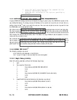
Страница 167: ...et system yet retaining debug control The need for a costly cable which brings out the DSP96002 footprint on an em ulator system is eliminated because of the easy access to the dedicated OnCE debug serial port Figure 10 1illustrates the block diagram of the OnCE serial interface 10 2 ON CHIP EMULATION OnCE PINOUT 10 2 1 Debug Serial Input Chip Status 0 DSI OS0 Serial data or commands are provided ...

Страница 168: ...0 pin provides information about the chip status describing why the debug mode cannot be entered in response to an external request The DSCK OS1 pin is output when not in the Debug Mode until the acknowledge signal is issued to the Command Controller When switching from output to input the pin is three stated In order to avoid any possible glitches an external pull down resistor should be attached...

Страница 169: ...contains the following blocks input shift register bit counter OnCE decoder and the status control register Figure 10 2 illustrates a block diagram of the OnCE se rial interface 10 3 1 OnCE Input Shift Register OISR The OnCE Input Shift Register is an 8 bit shift register that receives the serial data from the DSI line The data is clocked into the register on the falling edge of the clock applied ...

Страница 170: ...ead only 10 3 4 1 Program Memory Breakpoint Enable PBE0 PBE1 Bits 0 1 These control bits unmask program memory breakpoints allowing break point interrupts to occur when a program memory address is within the low and high program memory address registers and will select whether the breakpoint will be recognized for read or write accesses These bits are cleared on hardware reset PBE1 PBE0 Selection ...

Страница 171: ...emory breakpoints are enabled only for DMA accesses to program memory space 10 3 4 3 Data Memory Breakpoint Enable DBE0 DBE1 Bit 4 5 These control bits enable data memory breakpoints to occur when a data memory address is within the low and high data memory address registers and will select whether the breakpoint will be recognized for read or write accesses These bits are cleared on hardware rese...

Страница 172: ... This bit is cleared on hardware reset and when the OSCR is read 10 3 4 10 Software Debug Occurrence SWO Bit 19 This status bit is set when the debug mode of operation is entered due to the execution of the F DEBUGcc instruction with condition true This bit is cleared on hardware reset and when the OSCR is read 10 4 OnCE HARDWARE BREAKPOINT LOGIC Hardware breakpoints may be set on program memory o...

Страница 173: ...omparator will cause a logic true signal when the address on the bus is less than or equal to the high boundary If the low address comparator and high address compar ator both issue a logic true signal the address is within the address range and the breakpoint counter is decremented if the contents are greater than zero If zero the counter is not decremented and the break point exception occurs Co...

Страница 174: ...ts also occur after the execution of the instruction which formed the data memory address and the breakpoint counter has decremented to zero All breakpoint registers are controlled by the debug status and control register OSCR 10 4 2 Breakpoint Counter The breakpoint counter is useful for stopping at the nth iteration of a program loop or when the nth occur rence of a data memory access occurs Thi...

Страница 175: ...he program memory breakpoint lower limit OPLLR can only be read or written through the serial interface Before enabling breakpoints OPLLR must be loaded by the command controller 10 4 6 Program Memory High Address Comparator OPHC The Program Memory High Address Comparator compares the current program memory address stored by OPAL with the OPULR contents If OPULR is higher or equal than OPAL then t...

Страница 176: ...AL then the comparator delivers a signal indicating that address is higher than or equal to the low limit 10 4 14 Data Memory Breakpoint Counter ODBC The Data Memory Breakpoint Counter is a 32 bit counter which is loaded with a value equal to the number of times minus one that a data memory address should be accessed before a breakpoint is acknowledged On each data memory access the counter is dec...

Страница 177: ...of the serial clock set up time and must remain stable for at least 10 ns after the falling edge of the clock hold time The serial output line will clock out data from selected register as specified by the last command entered from the command controller The data bit value will be valid on the rising edge of the clock and will remain valid for at least 10 ns after the rising edge of the clock Afte...

Страница 178: ...interrupt processing 10 7 3 External Request During STOP Asserting D R when the chip is in the STOP state i e has executed a STOP instruction causes the chip to exit the STOP state and enter the Debug Mode After receiving the acknowledge the command con troller must negate D R Note that in this case the chip completes the execution of the STOP instruction and halts after the next instruction enter...

Страница 179: ...completing the execution of the instruc tion that caused the Breakpoint Counter decrement In case of breakpoints on Program memory addresses the breakpoint will be acknowledged immediately after the execution of the instruction that has caused the occurrence of the specified address In case of breakpoints on Data memory addresses the breakpoint will be acknowledged after the completion of the inst...

Страница 180: ...PILR 10 8 4 GDB Register OGDBR The GDB Register is a 32 bit latch that can only be read through the serial interface OGDBR is not actually required from a pipeline status restore point of view but is required as a means of passing information be tween the chip and the command controller OGDBR is mapped on the X internal I O space at address FFFFFFF0 Whenever the command controller needs a data wor...

Страница 181: ...MOTOROLA DSP96002 USER S MANUAL 10 15 Figure 10 8 Program Address Bus FIFO ...

Страница 182: ...ept for the FIFO pointer increment when reading the FIFO The last instruction executed before entering debug mode will be on the bottom of the FIFO Caution To ensure FIFO coherence a complete set of five reads of the FIFO must be per formed This is necessary due to the fact that each read increments the FIFO pointer thus pointing to the next location After five reads the pointer will point to the ...

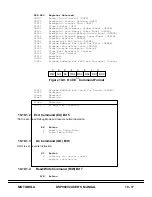
Страница 183: ...00 Debug Status Control OSCR 00001 Breakpoint Counter Program OPBC 00010 Breakpoint Counter Data ODBC 00011 Trace Counter OTC 00100 Breakpoint Data Memory Higher Equal ODULR 00101 Breakpoint Data Memory Lower Equal ODLLR 00110 Breakpoint Program Memory Higher Equal OPULR 00111 Breakpoint Program Memory Lower Equal OPLLR 01000 Transfer Register OGDBR 01001 Program Data Bus Latch OPDBR 01010 Program...

Страница 184: ... selects which method of communications will be used This allows a variety of different host computers to commu nicate with the controller circuit The controller circuit provides several important functions It acts as a DSP96002 serial debug port driver host computer command interpreter and DSP96002 controller The DSP96002 acts as a slave when in the debug mode and provides data only upon request ...

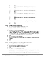
Страница 185: ...e register specified in the instruction are loaded in the GDB REGISTER The signal that marks the end of the instruction returns the chip to the halt state and an acknowledge is issued to the command controller 4 ACK 5 Send command READ GDB REGISTER ODEC selects GDB as source for serial data and an acknowledge is issued to the command controller 6 ACK 7 CLK 10 12 3 Displaying X memory area starting...

Страница 186: ... bit 2nd word of MOVE xxxx R0 the xxxx field After 32 bits have been received the PDB register drives the PDB ODEC releases the chip from the halt state and the instruction starts execution The signal that marks the end of the instruction returns the chip to the halt state and an acknowledge is issued to the command controller 15 ACK 16 Send command WRITE PDB REGISTER and GO no EX ODEC selects PDB...

Страница 187: ...C selects the on chip PAB register as the source for the PAB bus After the PAB was driven an acknowledge is is sued to the command controller 2 ACK 3 Send the 32 bits of the saved PIL instruction latch value After all the 32 bits have been received the PDB register drives the PDB ODEC causes the core to load the opcode An acknowledge is issued to the command controller 4 ACK 5 Send command WRITE P...

Страница 188: ...trace counter will count this instruction so the current trace counter may need to be corrected if the trace mode enable bit in the OSCR has been set e g After 32 bits have been received the PDB register drives the PDB ODEC releases the chip from the halt state and the Debug Mode bit in OSCR is cleared The chip executes first the jump instruction and will then fetch the instruction from the target...

Страница 189: ...mbined so that additional more restrictive classifications may be defined For example the instruction descriptions may use a memory alterable classification This refers to addressing modes which are both memory addressing modes and alterable addressing modes Memory alterable addressing modes use the effective address to address memory and exclude the imme diate addressing mode and the long displac...

Страница 190: ...ating point instructions The C bit is cleared during processor reset V Overflow Set if an arithmetic overflow occurs in a fixed point operation This indicates that the result is not representable in the destination size The V bit is not affected by floating point operations unless they have a fixed point result The overflow bit is also modified Register Direct Data or Control Register X Note 1 Add...

Страница 191: ...executing FABS S D will set the I bit The I bit is cleared during processor reset LR Local Reject The LR bit is only affected by the compare instructions CMP CMPG FCMP and FC MPG The LR bit is cleared during processor reset See the example for the FCMPG instruction for additional information R Reject The R bit is only affected by the compare instructions CMP CMPG FCMP and FC MPG The R bit is calcu...

Страница 192: ... tions are possible in practice due to the exclusive nature of the data types described by the condition codes The eight possible combinations are shown in Figure A 3 Figure A 4 details how each instruction affects the condition codes Figure A 4 gives the chip implemen tation viewpoint while the opcode descriptions in Section A 3 give the user viewpoint For example the Z bit computation for the CL...

Страница 193: ...Note 32 33 CMPG 1 Note 23 32 34 DEBUGcc DEC DO DOR ENDDO EOR 0 EXT 0 EXTB 0 FABS S FABS X FADD S FADD X FADDSUB S Note 9 10 11 FADDSUB X Note 9 10 11 FBcc FBScc FCLR FCMP Note 27 35 36 37 40 FCMPG 1 Note 27 35 38 39 40 FCMPM Note 27 40 FCOPYS S Symbols Set according to the standard definition by the result Not affected by the operation 0 Cleared 1 Set Set according to the special computation defin...

Страница 194: ... 13 14 FMPY FSUB X Note 12 13 14 FMPY S FMPY X FNEG S FNEG X FSCALE S FSCALE X FSEEDD FSEEDR FSUB S FSUB X FTFR S FTFR X FTRAPcc FTST GETEXP Note 16 IFcc IFcc U Note 21 ILLEGAL INC INT Note 16 17 24 INTRZ Note 16 17 24 NTU Note 16 24 41 INTURZ Note 16 24 41 Jcc JCLR JMP Figure A 4 Condition Codes Computation continued Symbols Set according to the standard definition by the result Not affected by t...

Страница 195: ... 6 7 8 22 MPYS Note 18 MPYU 0 Note 25 NEG NEGC Note 1 NOP NOT 0 OR 0 ORC 0 ORI Note 19 REP RESET ROL 0 Note 26 ROR 0 Note 26 RTI Note 20 RTR Note 20 RTS SETW 0 SPLIT 0 SPLITB 0 STOP SUB SUBC Note 1 TFR TRAPcc TST 0 WAIT Symbols Set according to the standard definition by the result Not affected by the operation 0 Cleared 1 Set Set according to the special computation definition by the result of th...

Страница 196: ...the addition is negative Cleared otherwise Note 11 Z Set if the result of the addition is zero Cleared otherwise Note 12 I Set if the result of the subtraction is infinity Cleared otherwise Note 13 N Set if the result of the subtraction is negative Cleared otherwise Note 14 Z Set if the result of the subtraction is zero Cleared otherwise Note 15 Z Set if the source operand is zero Cleared otherwis...

Страница 197: ...ffected otherwise Note 35 A Cleared if result is a NaN Cleared if result is negative and not zero Not affected otherwise Note 36 LR Cleared if result is positive zero or NaN Not affected otherwise Note 37 R Cleared if result is a NaN Not affected otherwise Note 38 R Cleared if result is a NaN Cleared if result is negative and not zero and LR was set Not affected otherwise Note 39 C Set if result i...

Страница 198: ...eration is a NaN Cleared otherwise The NAN bit is not affected by fixed point operations but is affected by some conversion instructions The NAN bit is cleared during processor reset UNCC Unordered Condition Set if a non aware floating point conditional instruction FBcc FJcc FFcc etc is executed when the NAN bit is set the unordered condition Not affected other wise The UNCC bit is cleared during ...

Страница 199: ...m as in one which was not aware This is not the case for inequality predicates In summary conditional predicates whose outcome may depend upon NaN awareness by the original author of the program are those involving inequalities The UNCC bit has been provided on the DSP96002 to aid in porting programs written in an IEEE non aware environment to the DSP96002 IEEE aware environment FBERR instructions...

Страница 200: ...NDDO EOR EXT EXTB FABS S 0 0 0 FABS X 0 0 0 FADD S 0 0 Note 18 FADD X 0 0 Note 18 FADDSUB S 0 0 Note 2 3 4 5 7 FADDSUB X 0 0 Note 2 3 4 5 7 FBcc FBScc FCLR 0 0 0 0 0 0 0 FCMP 0 0 0 0 0 0 FCMPG 0 0 0 0 0 0 FCMPM 0 0 0 0 0 0 FCOPYS S 0 0 0 Figure A 5 ER Exception Bits Computation SYMBOLS set according to the standard definition by the result not affected by the operation 0 cleared 1 set set accordin...

Страница 201: ...23 24 FMPY FSUB X 0 0 Notes 1 8 20 22 23 24 FMPY S 0 0 Note 6 FMPY X 0 0 Note 6 FNEG S 0 0 0 FNEG X 0 0 0 FSCALE S 0 0 0 FSCALE X 0 0 0 FSEEDD 0 0 0 0 FSEEDR 0 0 0 0 0 Note 31 FSUB S 0 0 Note 28 FSUB X 0 0 Note 28 FTFR S 0 0 0 FTFR X 0 0 0 FTRAPcc FTST 0 0 0 0 0 0 GETEXP 0 0 0 0 0 Notes 29 30 IFcc IFcc U Note 26 ILLEGAL INC INT 0 0 0 0 Notes 12 17 29 INTRZ 0 0 0 0 Notes 12 17 29 INTU 0 0 0 0 Notes...

Страница 202: ...16 MOVES Note 16 MOVETA MPYS MPYU NEG NEGC NOP NOTB OR ORC ORI Note 10 REP RESET ROL ROR RTI Note 11 RTR Note 11 RTS SETW SPLIT SPLITB STOP SUB SUBC TFR TRAPcc TST WAIT SYMBOLS set according to the standard definition by the result not affected by the operation 0 cleared 1 set set according to the special computation definition by the result of the operation Figure A 5 ER Exception Bits Computatio...

Страница 203: ...tion operand and INX DZ UNF OVF OPERR SNAN NAN or UNCC is selected then the selected bit will be set Not affected otherwise Note 16 All bits If SR is specified as a destination operand set according to the corresponding bit of the source operand Not affected otherwise Note 17 OPERR Set if the source operand is a NaN or infinity Also set if overflow occurred Cleared otherwise Note 18 OPERR Set if t...

Страница 204: ...nded result of an operation is not exact or if it overflows without an overflow trap SINX SINX v OVF v INX SDZ IEEE Division by Zero signaled if the dividend is a finite nonzero number and the divisor is zero SDZ SDZ v DZ SUNF IEEE Underflow signaled when both tininess and loss of accuracy have been detected Ti niness is detected before round see definition of UNF in the ER register Loss of accura...

Страница 205: ... 32 bits MR Mode register 8 bits ER Exception register 8 bits IER IEEE Exception register 8 bits CCR Condition code register 8 bits SR Status register 32 bits OMR Operating mode register 32 bits LA Hardware loop address register 32 bits LC Hardware loop counter 32 bits SP System stack pointer 32 bits SS System stack RAM 15 x 64 bits SSH Upper 32 bits of the contents of the current top of stack SSL...

Страница 206: ...teger source R Round optional rounding precision I1 I0 Interrupt priority level in SR LF Loop flag in SR Unary Negation Logical NOT PUSH Push onto SS PULL Pull from SS READ Read top of SS PURGE Delete top of SS Absolute Value Binary Addition Subtraction Multiplication Division v Logical Inclusive OR Logical AND Logical Exclusive OR Is transferred to Concatenation Miscellaneous Indicates an optiona...

Страница 207: ...nation operand low portion and store the result in the low portion of D Input Operand s Precision 32 bit integer Output Operand Precision 32 bit integer CCR Condition Codes C Not affected V Set if result overflows Cleared otherwise Z Set if result is zero Cleared otherwise N Set if result is negative Cleared otherwise I Not affected LR Not affected R Not affected A Not affected ER Status Bits Not ...

Страница 208: ...wo specified operands and store the result in the low portion of the destination operand D Input Operand s Precision 32 bit integer Output Operand Precision 32 bit integer CCR Condition Codes C Set if carry is generated from MSB of the result Cleared otherwise V Set if result overflows Cleared otherwise Z Set if result is zero Cleared otherwise N Set if result is negative Cleared otherwise I Not a...

Страница 209: ...dition code register and store the result in the low portion of destination operand D When doing multiple precision addition the higher precision long words of the input variables must be moved to the low portion of the Dn register Input Operand s Precision 32 bit integer Output Operand Precision 32 bit integer CCR Condition Codes C Set if carry is generated from the MSB of the result Cleared othe...

Страница 210: ...see the MOVE instruc tion description Description Logically AND the low portion of the two specified operands and store the result in the low portion of D Input Operand s Precision 32 bit integer Output Operand Precision 32 bit integer CCR Condition Codes C Not affected V Always cleared Z Set if result is zero Cleared otherwise N Set if result is negative Cleared otherwise I Not affected LR Not af...

Страница 211: ...ND the low portion of D with the logical complement of the low portion of S and store the result in the low portion of D Input Operand s Precision 32 bit integer Output Operand Precision 32 bit integer CCR Condition Codes C Not affected V Always cleared Z Set if result is zero Cleared otherwise N Set if result is negative Cleared otherwise I Not affected LR Not affected R Not affected A Not affect...

Страница 212: ...A 24 DSP96002 USER S MANUAL MOTOROLA Instruction Fields D d d d Dn L n n n where nnn 0 7 S s s s Dn L n n n where nnn 0 7 Timing 2 mv oscillator clock cycles Memory 1 mv program words ...

Страница 213: ...d Not affected otherwise R Cleared if bit 6 of the immediate operand is cleared Not affected otherwise A Cleared if bit 7 of the immediate operand is cleared Not affected otherwise For OMR MR IER ER operands C Not affected V Not affected Z Not affected N Not affected I Not affected LR Not affected R Not affected A Not affected ER Status Bits For ER operand INX Cleared if bit 0 of the immediate ope...

Страница 214: ...it 2 of the immediate operand is cleared Not affected otherwise SOVF Cleared if bit 3 of the immediate operand is cleared Not affected otherwise SIOP Cleared if bit 4 of the immediate operand is cleared Not affected otherwise For OMR MR ER CCR operands SINX Not affected SDZ Not affected SUNF Not affected SOVF Not affected SIOP Not affected Instruction Format AND I Byte D 0000 0001 0001 i i i i i i...

Страница 215: ...ed in the 11 LSBs of the high portion of S or by a 6 bit immediate field in the instruction The carry bit receives the Nth bit shifted out of the low portion of the source operand it is cleared for a shift count of zero N zeros are shifted into the LSBs of the destination operand If more than 32 bits are shifted zeros will be stored in D and the carry bit The result is stored in the low portion of...

Страница 216: ...EXTENSION OR IMMEDIATE LONG DATA 01 001n nnnn nddd 31 14 13 0 0000 0000 0000 0000 10 Instruction Fields u u D d d d Dn L n n n where nnn 0 7 S s s s Dn H n n n where nnn 0 7 N n n n n n n 0 0 0 0 0 0 0 1 0 0 0 0 0 1 2 0 0 0 0 1 0 62 1 1 1 1 1 0 63 1 1 1 1 1 1 Timing 2 mv oscillator clock cycles 2 oscillator clock cycles for ASL shift Memory 1 mv program words 1 program word for ASL shift Instructi...

Страница 217: ...n the 11 LSBs of the high portion of S or by a 6 bit immediate field in the instruction The carry bit receives the Nth bit shifted out of the low portion of the source operand it is cleared for a shift count of zero N copies of the MSB of the operand are shifted into the N MSBs of the destination operand If more than 32 bits are shifted copies of the MSB will be stored in D and the carry bit The r...

Страница 218: ...v oscillator clock cycles 2 oscillator clock cycles for ASR shift Memory 1 mv program words 1 program word for ASR shift DATA BUS MOVE FIELD 10 0000 uu11 1ddd 31 14 13 0 OPTIONAL EFFECTIVE ADDRESS EXTENSION OR IMMEDIATE LONG DATA DATA BUS MOVE FIELD 11 0sss 0011 1ddd 31 14 13 0 OPTIONAL EFFECTIVE ADDRESS EXTENSION OR IMMEDIATE LONG DATA 01 000n nnnn nddd 31 14 13 0 0000 0000 0000 0000 10 Instructi...

Страница 219: ... PC to the destination PC Short Displacement Long Dis placement and Address Register PC Relative addressing modes may be used The Short Displacement 15 bit data is sign extended to form the PC relative displacement See Section A 10 for restrictions cc may specify the following conditions Mnemonic Condition CC HS carry clear higher or same C 0 CS LO carry set lower C 1 EQ equal Z 1 GE greater or eq...

Страница 220: ... 1 MI 1 1 0 0 1 CC HS 0 1 0 1 0 CS LO 1 1 0 1 0 GE 0 1 0 1 1 LT 1 1 0 1 1 GT 0 1 1 0 0 LE 1 1 1 0 0 VC 0 1 1 0 1 VS 1 1 1 0 1 HI 0 1 1 1 0 LS 1 1 1 1 0 Timing 6 jx oscillator clock cycles Memory 1 ea program words 1c cccc 0000 0000 31 14 13 0 PC RELATIVE DISPLACEMENT 0000 0011 0000 0000 00 1c cccc 0000 0000 31 14 13 0 0000 0011 0000 001R 1c cccc 0aaa aaaa 31 14 13 0 0000 0011 10aa aaaa aa Instruct...

Страница 221: ...sted is selected by an immediate bit number 0 31 This instruction performs a read modify write operation on the destination operand and requires two destination accesses This instruction pro vides a test and change capability which is useful for synchronizing multiple processors using a shared memory See Section A 10 for restrictions CCR Condition Codes For destination operand SR C Changed if bit ...

Страница 222: ...2 is specified Not affected otherwise SNAN Changed if bit 13 is specified Not affected otherwise NAN Changed if bit 14 is specified Not affected otherwise UNCC Changed if bit 15 is specified Not affected otherwise For other destination operands INX Not affected DZ Not affected UNF Not affected OVF Not affected OPERR Not affected SNAN Not affected NAN Not affected UNCC Not affected IER Flags For de...

Страница 223: ...aaa 7 bits I O Short Address ppppppp 7 bits Memory Space S Bit Number b b b b b X Memory 0 Bit 0 31 n n n n n where nnnnn 0 31 Y Memory 1 aa 010S 000b bbbb 31 14 13 0 0000 0010 0110 0aaa aa 00 010S 000b bbbb 31 14 13 0 0000 0010 0101 MMMR pp 010S 000b bbbb 31 14 13 0 0000 0010 0110 1ppp pp d0 0100 000b bbbb 31 14 13 0 0000 0010 0111 dddd dd Instruction Format BCHG bit X pp BCHG bit Y pp Instructio...

Страница 224: ... 0 D9 L 0 1 0 0 0 0 1 D8 M 0 1 0 0 0 1 0 D9 M 0 1 0 0 0 1 1 D8 H 0 1 0 0 1 0 0 D9 H 0 1 0 0 1 0 1 D8 S 0 1 0 0 1 1 0 D9 S 0 1 0 0 1 1 1 R0 R7 0 1 0 1 n n n N0 N7 0 1 1 0 n n n M0 M7 0 1 1 1 n n n SR 1 1 1 1 0 0 1 OMR 1 1 1 1 0 1 0 SP 1 1 1 1 0 1 1 SSH 1 1 1 1 1 0 0 SSL 1 1 1 1 1 0 1 LA 1 1 1 1 1 1 0 LC 1 1 1 1 1 1 1 Timing 4 mvb oscillator clock cycles Memory 1 ea program words ...

Страница 225: ...ed by an immediate bit number 0 31 This instruction performs a read modify write operation on the destination operand and requires two destination accesses This instruction pro vides a test and clear capability which is useful for synchronizing multiple processors using a shared memory See Section A 10 for restrictions CCR Condition Codes For destination operand SR C Cleared if bit 0 is specified ...

Страница 226: ...2 is specified Not affected otherwise SNAN Cleared if bit 13 is specified Not affected otherwise NAN Cleared if bit 14 is specified Not affected otherwise UNCC Cleared if bit 15 is specified Not affected otherwise For other destination operands INX Not affected DZ Not affected UNF Not affected OVF Not affected OPERR Not affected SNAN Not affected NAN Not affected UNCC Not affected IER Flags For de...

Страница 227: ...aaa 7 bits I O Short Address ppppppp 7 bits aa 010S 000b bbbb 31 14 13 0 0000 0010 0010 0aaa aa 00 010S 000b bbbb 31 14 13 0 OPTIONAL EFFECTIVE ADDRESS EXTENSION 0000 0010 0001 MMMR pp 010S 000b bbbb 31 14 13 0 0000 0010 0010 1ppp pp d0 0100 000b bbbb 31 14 13 0 0000 0010 0011 dddd dd Memory Space S X Memory 0 Y Memory 1 Bit Number b b b b b Bit 0 31 n n n n n where nnnnn 0 31 Instruction Format B...

Страница 228: ... 0 D9 L 0 1 0 0 0 0 1 D8 M 0 1 0 0 0 1 0 D9 M 0 1 0 0 0 1 1 D8 H 0 1 0 0 1 0 0 D9 H 0 1 0 0 1 0 1 D8 S 0 1 0 0 1 1 0 D9 S 0 1 0 0 1 1 1 R0 R7 0 1 0 1 n n n N0 N7 0 1 1 0 n n n M0 M7 0 1 1 1 n n n SR 1 1 1 1 0 0 1 OMR 1 1 1 1 0 1 0 SP 1 1 1 1 0 1 1 SSH 1 1 1 1 1 0 0 SSL 1 1 1 1 1 0 1 LA 1 1 1 1 1 1 0 LC 1 1 1 1 1 1 1 Timing 4 mvb oscillator clock cycles Memory 1 ea program words ...

Страница 229: ...on Description Return the position of the source operand S leading one considered from left to right as a 2 s complement integer in the high portion of destination operand D If the source operand is zero then return 80000000 Input Operand s Precision 32 bit integer Output Operand Precision 32 bit integer CCR Condition Codes C Not affected V Always cleared Z Set if source operand is zero Cleared ot...

Страница 230: ...See Section A 10 for restrictions CCR Condition Codes Not affected ER Status Bits Not affected IER Flags Not affected Instruction Format BRA label short BRA Branch Always BRA Instruction Fields Rn R0 R7 Long PC Relative Displacement 32 bits Short PC Relative Displacement aaaaaaaaaaaaaaa 15 bits Timing 6 jx oscillator clock cycles Memory 1 ea program words 11 1111 0000 0000 31 14 13 0 PC RELATIVE D...

Страница 231: ... instruction If the tested bit is set the PC is incremented and program execution continues sequentially However the address register spec ified in the effective address field is always updated independently of the condition The displacement is a 2 s complement 32 bit integer that represents the relative distance from the current PC to the destination PC The 32 bit displacement is contained in the...

Страница 232: ...LACEMENT 0000 0010 1010 0aaa aa 00 010S 000b bbbb 31 14 13 0 PC RELATIVE DISPLACEMENT 0000 0010 1000 MMMR pp 010S 000b bbbb 31 14 13 0 PC RELATIVE DISPLACEMENT 0000 0010 1010 1ppp pp d0 0100 000b bbbb 31 14 13 0 PC RELATIVE DISPLACEMENT 0000 0010 1011 dddd dd Memory Space S X Memory 0 Y Memory 1 Bit Number b b b b b Bit 0 31 n n n n n where nnnnn 0 31 Instruction Format BRCLR bit X pp label BRCLR ...

Страница 233: ... 0 0 D9 L 0 1 0 0 0 0 1 D8 M 0 1 0 0 0 1 0 D9 M 0 1 0 0 0 1 1 D8 H 0 1 0 0 1 0 0 D9 H 0 1 0 0 1 0 1 D8 S 0 1 0 0 1 1 0 D9 S 0 1 0 0 1 1 1 R0 R7 0 1 0 1 n n n N0 N7 0 1 1 0 n n n M0 M7 0 1 1 1 n n n SR 1 1 1 1 0 0 1 OMR 1 1 1 1 0 1 0 SP 1 1 1 1 0 1 1 SSH 1 1 1 1 1 0 0 SSL 1 1 1 1 1 0 1 LA 1 1 1 1 1 1 0 LC 1 1 1 1 1 1 1 Timing 8 jx oscillator clock cycles Memory 2 program words ...

Страница 234: ...ruction If the tested bit is cleared the PC is incremented and program execution continues sequentially However the address register specified in the effective address field is always updated independently of the condition The displacement is a 2 s complement 32 bit integer that represents the relative distance from the current PC to the destination PC The 32 bit displacement is contained in the e...

Страница 235: ...LACEMENT 0000 0010 1010 0aaa aa 00 110S 000b bbbb 31 14 13 0 PC RELATIVE DISPLACEMENT 0000 0010 1000 MMMR pp 110S 000b bbbb 31 14 13 0 PC RELATIVE DISPLACEMENT 0000 0010 1010 1ppp pp d0 1100 000b bbbb 31 14 13 0 PC RELATIVE DISPLACEMENT 0000 0010 1011 dddd dd Memory Space S X Memory 0 Y Memory 1 Bit Number b b b b b Bit 0 31 n n n n n where nnnnn 0 31 Instruction Format BRSET bit X ea label BRSET ...

Страница 236: ... 0 0 D9 L 0 1 0 0 0 0 1 D8 M 0 1 0 0 0 1 0 D9 M 0 1 0 0 0 1 1 D8 H 0 1 0 0 1 0 0 D9 H 0 1 0 0 1 0 1 D8 S 0 1 0 0 1 1 0 D9 S 0 1 0 0 1 1 1 R0 R7 0 1 0 1 n n n N0 N7 0 1 1 0 n n n M0 M7 0 1 1 1 n n n SR 1 1 1 1 0 0 1 OMR 1 1 1 1 0 1 0 SP 1 1 1 1 0 1 1 SSH 1 1 1 1 1 0 0 SSL 1 1 1 1 1 0 1 LA 1 1 1 1 1 1 0 LC 1 1 1 1 1 1 1 Timing 8 jx oscillator clock cycles Memory 2 program words ...

Страница 237: ... PC is incremented and program execution continues sequentially The displacement is a 2 s complement 32 bit integer that represents the relative distance from the current PC to the destination PC Short Displace ment Long Displacement and Address Register PC Relative addressing modes may be used The Short Displacement 15 bit data is sign extended to form the PC relative displacement See Section A 1...

Страница 238: ...4 13 0 0000 0011 11aa aaaa aa Instruction Format BScc Rn Instruction Format BScc label Instruction Fields Rn R0 R7 Long Displacement 32 bits Short Displacement aaaaaaaaaaaaaaa 15 bits Mnemonic c c c c c Mnemonic c c c c c EQ 0 1 0 0 0 NE Q 1 1 0 0 0 PL 0 1 0 0 1 MI 1 1 0 0 1 CC HS 0 1 0 1 0 CS LO 1 1 0 1 0 GE 0 1 0 1 1 LT 1 1 0 1 1 GT 0 1 1 0 0 LE 1 1 1 0 0 VC 0 1 1 0 1 VS 1 1 1 0 1 HI 0 1 1 1 0 L...

Страница 239: ... at location PC displacement The PC contains the address of the next instruc tion If the tested bit is set the PC is incremented and program execution continues sequentially How ever the address register specified in the effective address field is always updated independently of the condition The displacement is a 2 s complement 32 bit integer that represents the relative distance from the current...

Страница 240: ...IVE DISPLACEMENT 0000 0010 1110 0aaa aa 00 010S 000b bbbb 31 14 13 0 PC RELATIVE DISPLACEMENT 0000 0010 1100 MMMR pp 010S 000b bbbb 31 14 13 0 PC RELATIVE DISPLACEMENT 0000 0010 1110 1ppp pp d0 0100 000b bbbb 31 14 13 0 PC RELATIVE DISPLACEMENT 0000 0010 1111 dddd dd Memory Space S X Memory 0 Y Memory 1 Bit Number b b b b b Bit 0 31 n n n n n where nnnnn 0 31 Instruction Format BSCLR bit X pp labe...

Страница 241: ...L 0 1 0 0 0 0 1 D8 M 0 1 0 0 0 1 0 D9 M 0 1 0 0 0 1 1 D8 H 0 1 0 0 1 0 0 D9 H 0 1 0 0 1 0 1 D8 S 0 1 0 0 1 1 0 D9 S 0 1 0 0 1 1 1 R0 R7 0 1 0 1 n n n N0 N7 0 1 1 0 n n n M0 M7 0 1 1 1 n n n SR 1 1 1 1 0 0 1 OMR 1 1 1 1 0 1 0 SP 1 1 1 1 0 1 1 SSH 1 1 1 1 1 0 0 SSL 1 1 1 1 1 0 1 LA 1 1 1 1 1 1 0 LC 1 1 1 1 1 1 1 Timing 8 jx oscillator clock cycles Memory 2 program words ...

Страница 242: ...ted is selected by an immediate bit number 0 31 This instruction performs a read modify write operation on the destination operand and requires two destination accesses This instruction pro vides a test and set capability which is useful for synchronizing multiple processors using a shared mem ory See Section A 10 for restrictions CCR Condition Codes For destination operand SR C Set if bit 0 is sp...

Страница 243: ... bit 12 is specified Not affected otherwise SNAN Set if bit 13 is specified Not affected otherwise NAN Set if bit 14 is specified Not affected otherwise UNCC Set if bit 15 is specified Not affected otherwise For other destination operands INX Not affected DZ Not affected UNF Not affected OVF Not affected OPERR Not affected SNAN Not affected NAN Not affected UNCC Not affected IER Flags For destinat...

Страница 244: ...aaa 7 bits I O Short Address ppppppp 7 bits aa 110S 000b bbbb 31 14 13 0 0000 0010 0010 0aaa aa 00 110S 000b bbbb 31 14 13 0 OPTIONAL EFFECTIVE ADDRESS EXTENSION 0000 0010 0000 MMMR pp 110S 000b bbbb 31 14 13 0 0000 0010 0010 1ppp pp d0 1100 000b bbbb 31 14 13 0 0000 0010 0011 dddd dd Memory Space S X Memory 0 Y Memory 1 Bit Number b b b b b Bit 0 31 n n n n n where nnnnn 0 31 Instruction Format B...

Страница 245: ... 0 D9 L 0 1 0 0 0 0 1 D8 M 0 1 0 0 0 1 0 D9 M 0 1 0 0 0 1 1 D8 H 0 1 0 0 1 0 0 D9 H 0 1 0 0 1 0 1 D8 S 0 1 0 0 1 1 0 D9 S 0 1 0 0 1 1 1 R0 R7 0 1 0 1 n n n N0 N7 0 1 1 0 n n n M0 M7 0 1 1 1 n n n SR 1 1 1 1 0 0 1 OMR 1 1 1 1 0 1 0 SP 1 1 1 1 0 1 1 SSH 1 1 1 1 1 0 0 SSL 1 1 1 1 1 0 1 LA 1 1 1 1 1 1 0 LC 1 1 1 1 1 1 1 Timing 4 mvb oscillator clock cycles Memory 1 ea program words ...

Страница 246: ...register are pushed onto the stack Program execution then continues at location PC displacement The PC contains the ad dress of the next instruction The displacement is a 2 s complement 32 bit integer that represents the relative distance from the current PC to the destination PC Short Displacement Long Displacement and Address Register PC Relative addressing modes may be used The Short Displaceme...

Страница 247: ...DSP96002 USER S MANUAL A 59 Instruction Fields Rn R0 R7 Long PC Relative Displacement 32 bits Short PC Relative Displacement aaaaaaaaaaaaaaa 15 bits Timing 6 jx oscillator clock cycles Memory 1 ea program words ...

Страница 248: ...C displacement The PC contains the address of the next instruction If the tested bit is cleared the PC is incremented and program execution continues sequentially However the address register specified in the effective address field is always updated independently of the condition The displacement is a 2 s complement 32 bit integer that represents the relative distance from the current PC to the d...

Страница 249: ...000 0010 1110 0aaa aa 00 110S 000b bbbb 31 14 13 0 PC RELATIVE DISPLACEMENT 0000 0010 1100 MMMR pp 110S 000b bbbb 31 14 13 0 PC RELATIVE DISPLACEMENT 0000 0010 1110 1ppp pp d0 1100 000b bbbb 31 14 13 0 PC RELATIVE DISPLACEMENT 0000 0010 1111 dddd dd Memory Space S X Memory 0 Y Memory 1 Bit Number b b b b b Bit 0 31 n n n n n where nnnnn 0 31 Instruction Format BSSET bit X pp label BSSET bit Y pp l...

Страница 250: ... 0 0 D9 L 0 1 0 0 0 0 1 D8 M 0 1 0 0 0 1 0 D9 M 0 1 0 0 0 1 1 D8 H 0 1 0 0 1 0 0 D9 H 0 1 0 0 1 0 1 D8 S 0 1 0 0 1 1 0 D9 S 0 1 0 0 1 1 1 R0 R7 0 1 0 1 n n n N0 N7 0 1 1 0 n n n M0 M7 0 1 1 1 n n n SR 1 1 1 1 0 0 1 OMR 1 1 1 1 0 1 0 SP 1 1 1 1 0 1 1 SSH 1 1 1 1 1 0 0 SSL 1 1 1 1 1 0 1 LA 1 1 1 1 1 1 0 LC 1 1 1 1 1 1 1 Timing 8 jx oscillator clock cycles Memory 2 program words ...

Страница 251: ...er Direct Absolute Short and I O Short addressing may also be used The bit to be tested is selected by an immediate bit number 0 31 When used with the appropriate rotate instructions this instruction is useful for serial to parallel conversions If the system stack register SSH is specified as a source operand the system stack pointer SP is postdec remented by 1 after SSH is read CCR Condition Code...

Страница 252: ...0000 0010 0110 0aaa aa 00 110S 000b bbbb 31 14 13 0 OPTIONAL EFFECTIVE ADDRESS EXTENSION 0000 0010 0100 MMMR pp 110S 000b bbbb 31 14 13 0 PC RELATIVE DISPLACEMENT 0000 0010 0110 1ppp pp d0 1100 000b bbbb 31 14 13 0 PC RELATIVE DISPLACEMENT 0000 0010 0111 dddd dd Memory Space S X Memory 0 Y Memory 1 Bit Number b b b b b Bit 0 31 n n n n n where nnnnn 0 31 Instruction Format BTST bit X ea BTST bit Y...

Страница 253: ... 0 D9 L 0 1 0 0 0 0 1 D8 M 0 1 0 0 0 1 0 D9 M 0 1 0 0 0 1 1 D8 H 0 1 0 0 1 0 0 D9 H 0 1 0 0 1 0 1 D8 S 0 1 0 0 1 1 0 D9 S 0 1 0 0 1 1 1 R0 R7 0 1 0 1 n n n N0 N7 0 1 1 0 n n n M0 M7 0 1 1 1 n n n SR 1 1 1 1 0 0 1 OMR 1 1 1 1 0 1 0 SP 1 1 1 1 0 1 1 SSH 1 1 1 1 1 0 0 SSL 1 1 1 1 1 0 1 LA 1 1 1 1 1 1 0 LC 1 1 1 1 1 1 1 Timing 4 mvb oscillator clock cycles Memory 1 ea program words ...

Страница 254: ...r Syntax CLR D move syntax see the MOVE instruction description Description The low portion of the destination operand is cleared to zero This instruction is implemented by executing ANDC D D Input Operand s Precision 32 bit integer Output Operand Precision 32 bit integer CCR Condition Codes C Not affected V Always cleared Z Always set N Always cleared I Not affected LR Not affected R Not affected...

Страница 255: ...hat the line segment will be trivially accepted if A is set and R 1 whereas the line will be trivially rejected if R is cleared and A 0 This choice of accept reject conditions was selected to permit the CCR to be initialized by a single ORI instruction ORI E0 CCR SET A R LR i e assume line is initially accepted and not rejected MOVE X R0 N0 D0 L Y R4 D1 S get X0 Xmin CMP D1 D0 X R0 N0 D0 L X0 Xmin...

Страница 256: ...on ER Status Bits Not affected IER Flags Not affected Instruction Format CMP S1 S2 move syntax see the MOVE instruction description 00 0sss uu11 1ddd 31 14 13 0 OPTIONAL EFFECTIVE ADDRESS EXTENSION OR IMMEDIATE LONG DATA DATA BUS MOVE FIELD Instruction Fields S1 s s s Dn L n n n where nnn 0 7 S2 u u D d d d Dn L n n n where nnn 0 7 Timing 2 mv oscillator clock cycles Memory 1 mv program words ...

Страница 257: ...l be trivially accepted if A is set and R 1 whereas the line will be trivially rejected if R is cleared and A 0 This choice of accept reject conditions was selected to permit the CCR to be initialized by a single ORI instruction ORI E0 CCR SET A R LR i e assume line is initially accepted and not rejected MOVE X R0 N0 D0 L Y R4 D1 S get X0 Xmin CMP D1 D0 X R0 N0 D0 L X0 Xmin get X1 CMPG D1 D0 X1 Xm...

Страница 258: ...tion ER Status Bits Not affected IER Flags Not affected Instruction Format CMPG S1 S2 move syntax see the MOVE instruction description 11 0sss 0110 1ddd 31 14 13 0 OPTIONAL EFFECTIVE ADDRESS EXTENSION OR IMMEDIATE LONG DATA DATA BUS MOVE FIELD Instruction Fields S1 s s s Dn L n n n where nnn 0 7 S2 d d d Dn L n n n where nnn 0 7 Timing 2 mv oscillator clock cycles Memory 1 mv program words ...

Страница 259: ... next instruction cc may specify the following conditions Mnemonic Condition CC HS carry clear higher or same C 0 CS LO carry set lower C 1 EQ equal Z 1 GE greater or equal N V 0 GT greater than Z v N V 0 HI higher Z v C 0 LE less or equal Z v N V 1 LS lower or same Z v C 1 LT less than N V 1 MI minus N 1 NE Q not equal Z 0 PL plus N 0 VC overflow clear V 0 VS overflow set V 1 AL always true n a C...

Страница 260: ...Mnemonic c c c c c EQ 0 1 0 0 0 NE Q 1 1 0 0 0 PL 0 1 0 0 1 MI 1 1 0 0 1 CC HS 0 1 0 1 0 CS LO 1 1 0 1 0 GE 0 1 0 1 1 LT 1 1 0 1 1 GT 0 1 1 0 0 LE 1 1 1 0 0 VC 0 1 1 0 1 VS 1 1 1 0 1 HI 0 1 1 1 0 LS 1 1 1 1 0 AL 1 1 1 1 1 Timing 4 oscillator clock cycles Memory 1 program words ...

Страница 261: ...erand The result is stored in the low portion of D Input Operand s Precision 32 bit integer Output Operand Precision 32 bit integer CCR Condition Codes C Set if a borrow is generated from the MSB of the result Cleared otherwise V Set if result overflows Cleared otherwise Z Set if result is zero Cleared otherwise N Set if result is negative Cleared otherwise I Not affected LR Not affected R Not aff...

Страница 262: ...less long displacement may be used to generate the effective address of the source operand Register Direct addressing mode may also be used If immediate short data is specified the LC is loaded with the zero extended 19 bit immediate data During the second instruction cycle the current contents of the program counter PC register and the status register SR are pushed onto the system stack The stack...

Страница 263: ...t the address of the instruction following the last instruction in the DO loop Note that LF is the only bit in the status register SR that is restored after a hardware DO loop has been exited Note The loop flag LF is cleared by a hardware reset Restrictions The end of loop comparison previously described actually occurs at instruction fetch time That is LA is being compared with PC when the instru...

Страница 264: ...the first instruction at the top of the DO loop uses that same address register The top instruction becomes the following instruction because of the loop construct Similarly since the DO instruction accesses the program controller registers the DO instruction must not be immediately proceeded by any of the following instructions Immediately before DO BCHG BCLR BSET LA LC SSH SSL or SP LEA to LA LC...

Страница 265: ...nd ahead of the end of loop execution instructions which change program flow or change the system stack may not be used near the end of the loop without some restrictions Proper DO loop operation is guaranteed if no instruction starting at address LA 2 LA 1 or LA specifies the program controller registers SR SP SSL LA LC or implicitly PC as a destination register or specifies SSH as a source or de...

Страница 266: ...1 0 0 0 0 1 D8 M 0 1 0 0 0 1 0 D9 M 0 1 0 0 0 1 1 D8 H 0 1 0 0 1 0 0 D9 H 0 1 0 0 1 0 1 D8 S 0 1 0 0 1 1 0 D9 S 0 1 0 0 1 1 1 R0 R7 0 1 0 1 n n n N0 N7 0 1 1 0 n n n M0 M7 0 1 1 1 n n n SR 1 1 1 1 0 0 1 OMR 1 1 1 1 0 1 0 SP 1 1 1 1 0 1 1 SSH 1 1 1 1 1 0 0 SSL 1 1 1 1 1 0 1 LA 1 1 1 1 1 1 0 LC 1 1 1 1 1 1 1 Timing 6 mv oscillator clock cycles Memory 2 program words 00 0000 1000 0000 31 14 13 0 ABSO...

Страница 267: ... which is loaded into the loop counter LC The DO loop is executed LC times If LC 0 the loop is executed 2 32 times All address register indirect addressing modes less Long Displacement may be used Register Direct addressing mode may also be used If immediate short data is specified the LC is loaded with the zero extended 19 bit immedi ate data During hardware loop operation each instruction is fet...

Страница 268: ...isters SR SP SSL LA LC or implicitly PC as a destination register or specifies SSH as a source or destination register Also SSH cannot be specified as a source register in the DOR instruction itself The assembler will generate a warning if the restricted instructions are found within their restricted boundaries See Section A 10 for the complete list of restrictions Implementation Notes DOR SP labe...

Страница 269: ... M 0 0 1 0 n n n D0 H D7 H 0 0 1 1 n n n D8 L 0 1 0 0 0 0 0 D9 L 0 1 0 0 0 0 1 D8 M 0 1 0 0 0 1 0 D9 M 0 1 0 0 0 1 1 D8 H 0 1 0 0 1 0 0 D9 H 0 1 0 0 1 0 1 D8 S 0 1 0 0 1 1 0 D9 S 0 1 0 0 1 1 1 R0 R7 0 1 0 1 n n n N0 N7 0 1 1 0 n n n M0 M7 0 1 1 1 n n n SR 1 1 1 1 0 0 1 OMR 1 1 1 1 0 1 0 SP 1 1 1 1 0 1 1 SSH 1 1 1 1 1 0 0 SSL 1 1 1 1 1 0 1 LA 1 1 1 1 1 1 0 LC 1 1 1 1 1 1 1 Timing 8 mv oscillator cl...

Страница 270: ...re purged from the system stack The loop address LA and the loop counter LC registers are them restored from the system stack Restrictions Due to pipelining and the fact that the ENDDO instruction accesses the program controller registers the ENDDO instruction must not be immediately preceded by any of the following instructions Immediately before ENDDO MOVEC to LA LC SR SSH SSL OR SP MOVEM to LA ...

Страница 271: ...OR S D move syntax see the MOVE in struction description Description Logically exclusive OR the low portion of the two specified operands and store the result in the low portion of D Input Operand s Precision 32 bit integer Output Operand Precision 32 bit integer CCR Condition Codes C Not affected V Always cleared Z Set if result is zero Cleared otherwise N Set if result is negative Cleared otherw...

Страница 272: ...16 Assembler Syntax EXT D move syntax see the MOVE in struction description Description Sign extend the lower 16 bits of D L into the upper 16 bits of D L Input Operand s Precision 16 bit integer Output Operand Precision 32 bit integer CCR Condition Codes C Not affected V Always cleared Z Set if result is zero Cleared otherwise N Set if result is negative Cleared otherwise I Not affected LR Not af...

Страница 273: ...Assembler Syntax EXTB D move syntax see the MOVE in struction description Description Sign extend the lower byte of D L into the upper 24 bits of D L Input Operand s Precision 8 bit integer Output Operand Precision 32 bit integer CCR Condition Codes C Not affected V Always cleared Z Set if result is zero Cleared otherwise N Set if result is negative Cleared otherwise I Not affected LR Not affected...

Страница 274: ...ion SP Floating Point CCR Condition Codes C Not affected V Not affected Z Set if result is zero Cleared otherwise N Always cleared I Set if result is infinity Cleared otherwise LR Not affected R Not affected A Not affected ER Status Bits INX Set if result is inexact Cleared otherwise DZ Always cleared UNF Set if result underflows Cleared otherwise OVF Set if result overflows Cleared otherwise OPER...

Страница 275: ... n n n where nnn 0 7 Timing 2 mv da oscillator clock cycles Memory 1 mv program words Instruction Format FABS S D move syntax see the MOVE instruction description 10 0001 uu11 0ddd 31 14 13 0 OPTIONAL EFFECTIVE ADDRESS EXTENSION OR IMMEDIATE LONG DATA DATA BUS MOVE FIELD ...

Страница 276: ...t Output Operand Precision SEP Floating Point CCR Condition Codes C Not affected V Not affected Z Set if result is zero Cleared otherwise N Always cleared I Set if result is infinity Cleared otherwise LR Not affected R Not affected A Not affected ER Status Bits INX Always cleared DZ Always cleared UNF Always cleared OVF Always cleared OPERR Always cleared SNAN Set if operand is a signaling NaN Cle...

Страница 277: ... n n n where nnn 0 7 Timing 2 mv da oscillator clock cycles Memory 1 mv program words Instruction Format FABS X D move syntax see the MOVE instruction description 10 0001 uu10 0ddd 31 14 13 0 OPTIONAL EFFECTIVE ADDRESS EXTENSION OR IMMEDIATE LONG DATA DATA BUS MOVE FIELD ...

Страница 278: ...lt is zero Cleared otherwise N Set if result is negative Cleared otherwise I Set if result is infinity Cleared otherwise LR Not affected R Not affected A Not affected ER Status Bits INX Set if result is inexact Cleared otherwise DZ Always cleared UNF Set if result underflows Cleared otherwise OVF Set if result overflows Cleared otherwise OPERR Set if operands are opposite signed infinities Cleared...

Страница 279: ...n Fields u u D d d d Dn n n n where nnn 0 7 S s s s Dn n n n where nnn 0 7 Timing 2 mv da oscillator clock cycles Memory 1 mv program words 01 0sss uu01 1ddd 31 14 13 0 OPTIONAL EFFECTIVE ADDRESS EXTENSION OR IMMEDIATE LONG DATA DATA BUS MOVE FIELD ...

Страница 280: ...s C Not affected V Not affected Z Set if result is zero Cleared otherwise N Set if result is negative Cleared otherwise I Set if result is infinity Cleared otherwise LR Not affected R Not affected A Not affected ER Status Bits INX Set if result is inexact Cleared otherwise DZ Always cleared UNF Set if result underflows Cleared otherwise OVF Set if result overflows Cleared otherwise OPERR Set if op...

Страница 281: ... 7 S s s s Dn n n n where nnn 0 7 Timing 2 mv da oscillator clock cycles Memory 1 mv program words Instruction Format FADD X S D move syntax see the MOVE instruction description 01 0sss uu00 0ddd 31 14 13 0 OPTIONAL EFFECTIVE ADDRESS EXTENSION OR IMMEDIATE LONG DATA DATA BUS MOVE FIELD ...

Страница 282: ...ffected A Not affected ER Status Bits INX Set if the addition or subtraction result is inexact Cleared otherwise DZ Always cleared UNF Set if the addition or subtraction result underflows Cleared otherwise OVF Set if the addition or subtraction result overflows Cleared otherwise OPERR Set if operands of the addition are opposite signed infinities or if the operands of the subtraction are like sign...

Страница 283: ...D2 d d d Dn n n n where nnn 0 7 Timing 2 mv da oscillator clock cycles Memory 1 mv program words Instruction Format FADDSUB S D1 D2 move syntax see the MOVE instruction description 01 0sss uu01 1ddd 31 14 13 0 OPTIONAL EFFECTIVE ADDRESS EXTENSION OR IMMEDIATE LONG DATA DATA BUS MOVE FIELD ...

Страница 284: ...affected A Not affected ER Status Bits INX Set if the addition or subtraction result is inexact Cleared otherwise DZ Always cleared UNF Set if the addition or subtraction result underflows Cleared otherwise OVF Set if the addition or subtraction result overflows Cleared otherwise OPERR Set if operands of the addition are opposite signed infinities or if the operands of the subtraction are like sig...

Страница 285: ...D2 d d d Dn n n n where nnn 0 7 Timing 2 mv da oscillator clock cycles Memory 1 mv program words Instruction Format FADDSUB X D1 D2 move syntax see the MOVE instruction description 01 0sss uu01 0ddd 31 14 13 0 OPTIONAL EFFECTIVE ADDRESS EXTENSION OR IMMEDIATE LONG DATA DATA BUS MOVE FIELD ...

Страница 286: ...he UNCC bit in the ER register if the NAN bit is set cc may specify the following conditions Non aware Mnemonic Condition Set UNCC EQ equal Z 1 No ERR error UNCC v SNAN v OPERR v No OVF v UNF v DZ 1 GE greater than or equal NAN v N Z 0 Yes GL greater or less than NAN v Z 0 Yes GLE greater less or equal NAN 0 Yes GT greater than NAN v Z v N 0 Yes INF infinity I 1 Yes LE less than or equal NAN v N v...

Страница 287: ...cted SDZ Not affected SUNF Not affected SOVF Not affected SIOP Set if NAN is set and a non aware floating point condition is tested cc conditions marked YES above Not affected otherwise Instruction Format FBcc label short Instruction Fields 1c cccc 0000 0000 31 14 13 0 PC RELATIVE DISPLACEMENT 0000 0011 0000 0000 00 1c cccc 0000 0000 31 14 13 0 PC RELATIVE DISPLACEMENT 0000 0011 0000 001R 1c cccc ...

Страница 288: ...c c GT 0 0 0 0 0 NGT 1 0 0 0 0 LT 0 0 0 0 1 NLT 1 0 0 0 1 GE 0 0 0 1 0 NGE 1 0 0 1 0 LE 0 0 0 1 1 NLE 1 0 0 1 1 GL 0 0 1 0 0 NGL 1 0 1 0 0 INF 0 0 1 0 1 NINF 1 0 1 0 1 GLE 0 0 1 1 0 NGLE 1 0 1 1 0 OR 0 0 1 1 1 UN 1 0 1 1 1 EQ 0 1 0 0 0 NE Q 1 1 0 0 0 PL 0 1 0 0 1 MI 1 1 0 0 1 ERR 0 1 1 1 1 Timing 6 jx oscillator clock cycles Memory 1 ea program words ...

Страница 289: ...isplacement and Ad dress Register PC Relative addressing modes may be used The Short Displacement 15 bit data is sign extended to form the PC relative displacement The PC points to the next instruction when it is added to the displacement See Section A 10 for restrictions Non aware floating point conditions set the SIOP flag in the IER and the UNCC bit in the ER if the NAN bit is set This action o...

Страница 290: ...r than NAN v Z v N 1 Yes NINF not infinity I 0 Yes NLE not less than or equal NAN v N v Z 1 Yes NLT not less than NAN v Z v N 1 Yes OR ordered NAN 0 No PL plus N 0 No UN unordered NAN 1 No Note The operands for the ERR condition are taken from the ER register See description of UNcc bit in Section A 4 CCR Condition Codes Not affected ER Status Bits INX Not affected DZ Not affected UNF Not affected...

Страница 291: ...0 NGLE 1 0 1 1 0 OR 0 0 1 1 1 UN 1 0 1 1 1 EQ 0 1 0 0 0 NE Q 1 1 0 0 0 PL 0 1 0 0 1 MI 1 1 0 0 1 ERR 0 1 1 1 1 Timing 6 jx oscillator clock cycles Memory 1 ea program words Instruction Format 1c cccc 0000 0000 31 14 13 0 OPTIONAL LONG DISPLACEMENT EXTENSION 0000 0011 0100 0000 00 1c cccc 0000 0000 31 14 13 0 OPTIONAL LONG DISPLACEMENT EXTENSION 0000 0011 0100 001R 1c cccc 0aaa aaaa 31 14 13 0 OPTI...

Страница 292: ...Floating Point CCR Condition Codes C Not affected V Not affected Z Always set N Always cleared I Always cleared LR Not affected R Not affected A Not affected ER Status Bits INX Always cleared DZ Always cleared UNF Always cleared OVF Always cleared OPERR Always cleared SNAN Not affected NAN Always cleared UNCC Always cleared IER Flags Not affected Instruction Format FCLR D move syntax see the MOVE ...

Страница 293: ...MOTOROLA DSP96002 USER S MANUAL A 105 Instruction Fields u u D d d d Dn n n n where nnn 0 7 Timing 2 mv da oscillator clock cycles Memory 1 mv program words ...

Страница 294: ... is no rounding and therefore the condition code bits are set as suming an infinite precision result C Not affected V Not affected Z Set if source operands are equal Cleared otherwise N Set if result is negative Cleared otherwise I Set if anyone of the operands is infinity Cleared otherwise LR Cleared if result is positive zero or NaN if cleared first print accepted see the FC MPG example Not affe...

Страница 295: ... u u S2 d d d Dn n n n where nnn 0 7 Timing 2 mv da oscillator clock cycles Memory 1 mv program words Instruction Format FCMP S1 S2 move syntax see the MOVE instruction description 01 1sss uu01 0ddd 31 14 13 0 OPTIONAL EFFECTIVE ADDRESS EXTENSION OR IMMEDIATE LONG DATA DATA BUS MOVE FIELD ...

Страница 296: ...ffer ences are particularly useful in performing clipping operations in graphics applications In the code seg ment the FCMP instruction tests the first point of a line X0 against Xmin and sets LR accordingly the FC MPG instruction tests the second point of a line X1 against Xmin and sets R depending on the condition of LR Note that the line segment will be trivially accepted if A is set and R 1 wh...

Страница 297: ...or the next FCMP FCMPG combination R Cleared if result is a NaN Cleared if result is negative and not zero and LR was set i e first point was rejected Not affected otherwise A Cleared if result is a NaN Cleared if result is negative and not zero Not affected otherwise ER Status Bits IER Flags Flags changed according to standard definition Instruction Format FCMPG S1 S2 move syntax see the MOVE ins...

Страница 298: ...rue even if S1 S2 are infinity Input Operand s Precision SEP Floating Point Output Operand Precision n a CCR Condition Codes Note Since there is no destination there is no rounding and therefore the condition code bits are set as suming an infiite precision result C Not affected V Not affected Z Set if source operands are equal Cleared otherwise N Set if result is negative Cleared otherwise I Set ...

Страница 299: ...n 0 7 Timing 2 mv da oscillator clock cycles Memory 1 mv program words IER Flags Flags changed according to standard definition Instruction Format FCMPM S1 S2 move syntax see the MOVE instruction description 01 1sss uu01 1ddd 31 14 13 0 OPTIONAL EFFECTIVE ADDRESS EXTENSION OR IMMEDIATE LONG DATA DATA BUS MOVE FIELD ...

Страница 300: ...et if result is negative Cleared otherwise I Set if result is infinity Cleared otherwise LR Not affected R Not affected A Not affected ER Status Bits INX Set if result is inexact Cleared otherwise DZ Always cleared UNF Set if result underflows Cleared otherwise OVF Set if result overflows Cleared otherwise OPERR Always cleared SNAN Set if operand is a signaling NaN Cleared otherwise NAN Set if res...

Страница 301: ...u u D d d d Dn n n n where nnn 0 7 Timing 2 mv da oscillator clock cycles Memory 1 mv program words Instruction Format FCOPYS S S D move syntax see the MOVE instruction description 01 1sss uu11 1ddd 31 14 13 0 OPTIONAL EFFECTIVE ADDRESS EXTENSION OR IMMEDIATE LONG DATA DATA BUS MOVE FIELD ...

Страница 302: ...sion SEP Floating Point Output Operand Precision SEP Floating Point CCR Condition Codes C Not affected V Not affected Z Set if result is zero Cleared otherwise N Set if result is negative Cleared otherwise I Set if result is infinity Cleared otherwise LR Not affected R Not affected A Not affected ER Status Bits INX Always cleared DZ Always cleared UNF Always cleared OVF Always cleared OPERR Always...

Страница 303: ...0 7 S s s s Dn n n n where nnn 0 7 Timing 2 mv da oscillator clock cycles Memory 1 mv program words Instruction Format FCOPYS X S D move syntax see the MOVE instruction description 01 0sss uu11 1ddd 31 14 13 0 OPTIONAL EFFECTIVE ADDRESS EXTENSION OR IMMEDIATE LONG DATA DATA BUS MOVE FIELD ...

Страница 304: ...DZ 1 GE greater than or equal NAN v N Z 0 Yes GL greater or less than NAN v Z 0 Yes GLE greater less or equal NAN 0 Yes GT greater than NAN v Z v N 0 Yes INF infinity I 1 Yes LE less than or equal NAN v N v Z 0 Yes LT less than NAN v Z v N 0 Yes MI minus N 1 No NE Q not equal Z 0 No NGE not greater than or equal NAN v N Z 1 Yes NGL not greater or less than NAN v Z 1 Yes NGLE not greater less or eq...

Страница 305: ...et and a non aware floating point condition is tested cc conditions marked YES above Not affected otherwise Instruction Format Instruction Fields Mnemonic c c c c c Mnemonic c c c c c GT 0 0 0 0 0 NGT 1 0 0 0 0 LT 0 0 0 0 1 NLT 1 0 0 0 1 GE 0 0 0 1 0 NGE 1 0 0 1 0 LE 0 0 0 1 1 NLE 1 0 0 1 1 GL 0 0 1 0 0 NGL 1 0 1 0 0 INF 0 0 1 0 1 NINF 1 0 1 0 1 GLE 0 0 1 1 0 NGLE 1 0 1 1 0 OR 0 0 1 1 1 UN 1 0 1 1...

Страница 306: ...dless of whether the mantissa is denormalized or not As an example of the use of FGETMAN GETEXP and FSCALE consider decomposing a floating point number into its mantissa and unbiased exponent and then recreating the original floating point number FGETMAN D0 D1 extract normalized mantissa GETEXP D0 D2 extract unbiased exponent MOVE D2 L D2 H move unbiased exponent FSCALE X D2 H D1 scale original ma...

Страница 307: ...operand is infinity Cleared otherwise SNAN Set if operand is a signaling NaN Cleared otherwise NAN Set if result is a NaN Cleared otherwise UNCC Always cleared IER Flags Flags changed according to standard definition Instruction Format FGETMAN S D move syntax see the MOVE instruction description Instruction Fields u u D d d d Dn n n n where nnn 0 7 S s s s Dn n n n where nnn 0 7 Timing 2 mv da osc...

Страница 308: ...50 rounds to 110 0 Input Operand s Precision SEP Floating Point Output Operand Precision SEP Floating Point CCR Condition Codes C Not affected V Not affected Z Set if result is zero Cleared otherwise N Set if result is negative Cleared otherwise I Set if result is infinity Cleared otherwise LR Not affected R Not affected A Not affected ER Status Bits INX Set if result is inexact Cleared otherwise ...

Страница 309: ... s s Dn n n n where nnn 0 7 Timing 2 mv da oscillator clock cycles Memory 1 mv program words Instruction Format FINT S D move syntax see the MOVE instruction description 01 1sss uu11 0ddd 31 14 13 0 OPTIONAL EFFECTIVE ADDRESS EXTENSION OR IMMEDIATE LONG DATA DATA BUS MOVE FIELD ...

Страница 310: ...e floating point con ditions set the SIOP flag in the IER register and the UNCC bit in the ER register if the NAN bit is set cc may specify the following conditions Non aware Mnemonic Condition Set UNCC EQ equal Z 1 No ERR error UNCC v SNAN v OPERR v No OVF v UNF v DZ 1 GE greater than or equal NAN v N Z 0 Yes GL greater or less than NAN v Z 0 Yes GLE greater less or equal NAN 0 Yes GT greater tha...

Страница 311: ...is tested cc conditions marked YES above Not affected otherwise IER Flags SINX Not affected SDZ Not affected SUNF Not affected SOVF Not affected SIOP Set if NAN is set and a non aware floating point condition is tested cc conditions marked YES above Not affected otherwise 1c cccc 1aaa aaaa 31 14 13 0 0000 0011 10aa aaaa aa 1c cccc 1000 0000 31 14 13 0 OPTIONAL EFFECTIVE ADDRESS EXTENSION 0000 0011...

Страница 312: ...onic c c c c c Mnemonic c c c c c GT 0 0 0 0 0 NGT 1 0 0 0 0 LT 0 0 0 0 1 NLT 1 0 0 0 1 GE 0 0 0 1 0 NGE 1 0 0 1 0 LE 0 0 0 1 1 NLE 1 0 0 1 1 GL 0 0 1 0 0 NGL 1 0 1 0 0 INF 0 0 1 0 1 NINF 1 0 1 0 1 GLE 0 0 1 1 0 NGLE 1 0 1 1 0 OR 0 0 1 1 1 UN 1 0 1 1 1 EQ 0 1 0 0 0 NE Q 1 1 0 0 0 PL 0 1 0 0 1 MI 1 1 0 0 1 ERR 0 1 1 1 1 Timing 6 jx oscillator clock cycles Memory 1 ea program words ...

Страница 313: ...are floating point condi tions set the SIOP flag in the IER and the UNCC bit in the ER if the NAN bit is set This action occurs before stacking the status register when the specified non aware floating point condition is true cc may specify the following conditions Non aware Mnemonic Condition Set UNCC EQ equal Z 1 No ERR error UNCC v SNAN v OPERR v No OVF v UNF v DZ 1 GE greater than or equal NAN...

Страница 314: ...ked YES above Not affected otherwise IER Flags SINX Not affected SDZ Not affected SUNF Not affected SOVF Not affected SIOP Set if NAN is set and a non aware floating point condition is tested cc conditions marked YES above Not affected otherwise Instruction Fields Instruction Format FJScc label short 1c cccc 1aaa aaaa 31 14 13 0 0000 0011 11aa aaaa aa 1c cccc 1000 0000 31 14 13 0 OPTIONAL EFFECTIV...

Страница 315: ...c c Mnemonic c c c c c GT 0 0 0 0 0 NGT 1 0 0 0 0 LT 0 0 0 0 1 NLT 1 0 0 0 1 GE 0 0 0 1 0 NGE 1 0 0 1 0 LE 0 0 0 1 1 NLE 1 0 0 1 1 GL 0 0 1 0 0 NGL 1 0 1 0 0 INF 0 0 1 0 1 NINF 1 0 1 0 1 GLE 0 0 1 1 0 NGLE 1 0 1 1 0 OR 0 0 1 1 1 UN 1 0 1 1 1 EQ 0 1 0 0 0 NE Q 1 1 0 0 0 PL 0 1 0 0 1 MI 1 1 0 0 1 ERR 0 1 1 1 1 Timing 2 mv da oscillator clock cycles Memory 1 mv program words ...

Страница 316: ... store the result in the operand D Input Operand s Precision 32 bit 2 s complement integer Output Operand Precision SP Floating Point CCR Condition Codes C Not affected V Not affected Z Set if result is zero Cleared otherwise N Set if result is negative Cleared otherwise I Always cleared LR Not affected R Not affected A Not affected ER Status Bits INX Set if result is inexact Cleared otherwise DZ ...

Страница 317: ... n n n where nnn 0 7 Timing 2 mv da oscillator clock cycles Memory 1 mv program words Instruction Format FLOAT S D move syntax see the MOVE instruction description 10 0100 uu11 0ddd 31 14 13 0 OPTIONAL EFFECTIVE ADDRESS EXTENSION OR IMMEDIATE LONG DATA DATA BUS MOVE FIELD ...

Страница 318: ...n the operand D The rounding precision is SEP Input Operand s Precision 32 bit 2 s complement integer Output Operand Precision SEP Floating Point CCR Condition Codes C Not affected V Not affected Z Set if result is zero Cleared otherwise N Set if result is negative Cleared otherwise I Always cleared LR Not affected R Not affected A Not affected ER Status Bits INX Always cleared DZ Always cleared U...

Страница 319: ...nn 0 7 S s s s Dn n n n where nnn 0 7 Timing 2 mv da oscillator clock cycles Memory 1 mv program words Instruction Format FLOAT X D move syntax see the MOVE instruction description 10 0100 uu10 0ddd 31 14 13 0 OPTIONAL EFFECTIVE ADDRESS EXTENSION OR IMMEDIATE LONG DATA DATA BUS MOVE FIELD ...

Страница 320: ... single precision and store the result in the operand D Input Operand s Precision 32 bit unsigned integer Output Operand Precision SP Floating Point CCR Condition Codes C Not affected V Not affected Z Set if result is zero Cleared otherwise N Always cleared I Always cleared LR Not affected R Not affected A Not affected ER Status Bits INX Set if result is inexact Cleared otherwise DZ Always cleared...

Страница 321: ... n n n where nnn 0 7 Timing 2 mv da oscillator clock cycles Memory 1 mv program words Instruction Format FLOATU S D move syntax see the MOVE instruction description 10 0101 uu11 0ddd 31 14 13 0 OPTIONAL EFFECTIVE ADDRESS EXTENSION OR IMMEDIATE LONG DATA DATA BUS MOVE FIELD ...

Страница 322: ... is zero Cleared otherwise N Always cleared I Always cleared LR Not affected R Not affected A Not affected ER Status Bits INX Always cleared DZ Always cleared UNF Always cleared OVF Always cleared OPERR Always cleared SNAN Always cleared NAN Always cleared UNCC Always cleared IER Flags Flags changed according to standard definition Assembler Syntax FLOATU X D move syntax see the MOVE in struction ...

Страница 323: ...MOTOROLA DSP96002 USER S MANUAL A 135 Instruction Fields u u D ddd Dnnnn where nnn 0 7 Timing 2 mv da oscillator clock cycles Memory 1 mv program words ...

Страница 324: ...the round ing mode does not need to be saved changed and recalled This is particularly useful when using C since FLOOR is a standard C function Input Operand s Precision SEP Floating Point Output Operand Precision SEP Floating Point CCR Condition Codes C Not affected V Not affected Z Set if result is zero Cleared otherwise N Set if result is negative Cleared otherwise I Set if result is infinity C...

Страница 325: ...nnn 0 7 Timing 2 mv da oscillator clock cycles Memory 1 mv program words IER Flags Flags changed according to standard definition Instruction Format FLOOR S D move syntax see the MOVE instruction description 01 0sss uu11 0ddd 31 14 13 0 OPTIONAL EFFECTIVE ADDRESS EXTENSION OR IMMEDIATE LONG DATA DATA BUS MOVE FIELD ...

Страница 326: ...and Precision SP Floating Point Multiplication Output Operand Precision as indicated by MP CCR Condition Codes C Not affected V Not affected Z Set if result of the addition is zero Cleared otherwise N Set if result of the addition is negative Cleared otherwise I Set if result of the addition is infinity Cleared otherwise LR Not affected R Not affected A Not affected ER Status Bits INX Set if the r...

Страница 327: ...ction de scription Instruction Fields D1 D D Dn n n where nn 0 3 D2 d d Dn n n where nn 0 3 S3 s s s Dn n n n where nnn 0 7 S1 S2 Q QQ Q D0 D4 0 0 0 0 D4 D4 0 0 0 1 D4 D5 0 0 1 0 D4 D6 0 0 1 1 D5 D6 0 1 0 0 D4 D7 0 1 0 1 D5 D7 0 1 1 0 D6 D7 0 1 1 1 D4 D8 1 0 0 0 D5 D8 1 0 0 1 D6 D8 1 0 1 0 D7 D8 1 0 1 1 D4 D9 1 1 0 0 D5 D9 1 1 0 1 D6 D9 1 1 1 0 D7 D9 1 1 1 1 Timing 2 mv da oscillator clock cycles ...

Страница 328: ... is infinity Cleared otherwise LR Not affected R Not affected A Not affected ER Status Bits INX Set if the result of the addition or the multiplication is inexact Cleared otherwise DZ Always cleared UNF Set if the result of the addition or the multiplication underflows Cleared otherwise OVF Set if the result of the addition or the multiplication overflows Cleared otherwise OPERR Set if one of the ...

Страница 329: ... D Dn n n where nn 0 3 D2 d d Dn n n where nn 0 3 S3 s s s Dn n n n where nnn 0 7 S1 S2 Q QQ Q D0 D4 0 0 0 0 D4 D4 0 0 0 1 D4 D5 0 0 1 0 D4 D6 0 0 1 1 D5 D6 0 1 0 0 D4 D7 0 1 0 1 D5 D7 0 1 1 0 D6 D7 0 1 1 1 D4 D8 1 0 0 0 D5 D8 1 0 0 1 D6 D8 1 0 1 0 D7 D8 1 0 1 1 D4 D9 1 1 0 0 D5 D9 1 1 0 1 D6 D9 1 1 1 0 D7 D9 1 1 1 1 Timing 2 mv da oscillator clock cycles Memory 1 mv program words 00 0sss ddQQ QQD...

Страница 330: ...ion in register D3 Typically if the result of the multiplication will be used immediately follow ing a data ALU instruction such as FADD i e equivalent to an FMAC the maximum precision MP 1 will be programmed However if the product is to be stored then single precision MP 0 rounding will be used For the special case of s D the result can be 0 or 0 the sign of the resulting zero will be the sign of...

Страница 331: ...d otherwise SNAN Set if anyone of the source operands is a signaling NaN Cleared otherwise NAN Set if result of the addition is a NaN Cleared otherwise UNCC Always cleared IER Flags Flags changed according to standard definition Instruction Format Instruction Fields D1 D D Dn n n where nn 0 3 D2 d d Dn n n where nn 0 3 S3 s s s Dn n n n where nnn 0 7 10 1sss ddQQ QQDD 31 14 13 0 OPTIONAL EFFECTIVE...

Страница 332: ...result of the addition in register D2 and of the subtraction in register D3 Typically if the result of the multiplication will be used immediately following FADD i e equivalent to an FMAC the maximum precision MP 1 will be programmed For the special case of s D the result can be 0 or 0 the sign of the resulting zero will be the sign of the input operand in D Input Operand s Precision SEP Floating ...

Страница 333: ...d otherwise NAN Set if result of the addition is a NaN Cleared otherwise UNCC Always cleared IER Flags Flags changed according to standard definition Instruction Fields D1 D D Dn n n where nn 0 3 D2 d d Dn n n where nn 0 3 S3 s s s Dn n n n where nnn 0 7 10 0sss ddQQ QQDD 31 14 13 0 OPTIONAL EFFECTIVE ADDRESS EXTENSION OR IMMEDIATE LONG DATA DATA BUS MOVE FIELD Instruction Format FMPY S1 S2 D1 FAD...

Страница 334: ...n FMAC the maximum precision MP 1 will be programmed For the special case of s D the result can be 0 or 0 the sign of the resulting zero will be the sign of the input operand in D Input Operand s Precision SEP Floating Point Subtraction Output Operand Precision SP Floating Point Multiplication Output Operand Precision as indicated by MP CCR Condition Codes C Not affected V Not affected Z Set if re...

Страница 335: ...nstruction Fields D1 D D Dn n n where nn 0 3 D2 d d Dn n n where nn 0 3 S3 s s s Dn n n n where nnn 0 7 S1 S2 Q QQ Q D0 D4 0 0 0 0 D4 D4 0 0 0 1 D4 D5 0 0 1 0 D4 D6 0 0 1 1 D5 D6 0 1 0 0 D4 D7 0 1 0 1 D5 D7 0 1 1 0 D6 D7 0 1 1 1 D4 D8 1 0 0 0 D5 D8 1 0 0 1 D6 D8 1 0 1 0 D7 D8 1 0 1 1 D4 D9 1 1 0 0 D5 D9 1 1 0 1 D6 D9 1 1 1 0 D7 D9 1 1 1 1 Timing 2 mv da oscillator clock cycles Memory 1 mv program ...

Страница 336: ...A 148 DSP96002 USER S MANUAL MOTOROLA FMPY S2 S1 D1 FSUB S S3 D2 move syntax see the MOVE instruction de scription ...

Страница 337: ...MOTOROLA DSP96002 USER S MANUAL A 149 ...

Страница 338: ...recision SEP Floating Point Subtraction Output Operand Precision SEP Floating Point Multiplication Output Operand Precision SEP Floating Point CCR Condition Codes C Not affected V Not affected Z Set if result of the subtraction is zero Cleared otherwise N Set if result of the subtraction is negative Cleared otherwise I Set if result of the subtraction is infinity Cleared otherwise LR Not affected ...

Страница 339: ...ction de scription Instruction Fields D1 D D Dn n n where nn 0 3 D2 d d Dn n n where nn 0 3 S3 s s s Dn n n n where nnn 0 7 S1 S2 Q QQ Q D0 D4 0 0 0 0 D4 D4 0 0 0 1 D4 D5 0 0 1 0 D4 D6 0 0 1 1 D5 D6 0 1 0 0 D4 D7 0 1 0 1 D5 D7 0 1 1 0 D6 D7 0 1 1 1 D4 D8 1 0 0 0 D5 D8 1 0 0 1 D6 D8 1 0 1 0 D7 D8 1 0 1 1 D4 D9 1 1 0 0 D5 D9 1 1 0 1 D6 D9 1 1 1 0 D7 D9 1 1 1 1 Timing 2 mv da oscillator clock cycles ...

Страница 340: ...tput Operand Precision SP Floating Point CCR Condition Codes C Not affected V Not affected Z Set if result is zero Cleared otherwise N Set if result is negative Cleared otherwise I Set if result is infinity Cleared otherwise LR Not affected R Not affected A Not affected ER Status Bits INX Set if result is inexact Cleared otherwise DZ Always cleared UNF Set if result underflows Cleared otherwise OV...

Страница 341: ...ory 1 mv program words Instruction Format FMPY S S1 S2 D move syntax see the MOVE instruction description 11 1sss SSS1 0ddd 31 14 13 0 OPTIONAL EFFECTIVE ADDRESS EXTENSION OR IMMEDIATE LONG DATA DATA BUS MOVE FIELD 11 0sss 11S1 0ddd OPTIONAL EFFECTIVE ADDRESS EXTENSION OR IMMEDIATE LONG DATA DATA BUS MOVE FIELD 31 14 13 0 Instruction Format FMPY S S1 S2 8 9 D move syntax see the MOVE instruction d...

Страница 342: ...nt Output Operand Precision SEP Floating Point CCR Condition Codes C Not affected V Not affected Z Set if result is zero Cleared otherwise N Set if result is negative Cleared otherwise I Set if result is infinity Cleared otherwise LR Not affected R Not affected A Not affected ER Status Bits INX Set if result is inexact Cleared otherwise DZ Always cleared UNF Set if result underflows Cleared otherw...

Страница 343: ... 13 0 OPTIONAL EFFECTIVE ADDRESS EXTENSION OR IMMEDIATE LONG DATA DATA BUS MOVE FIELD 31 14 13 0 Instruction Fields S1 s s s Dn n n n where nnn 0 7 S2 S S S Dn n n n where nnn 0 7 S2 s D8 0 D9 1 D d d d Dn n n n where nnn 0 7 Timing 2 mv da oscillator clock cycles Memory 1 mv program words Instruction Format FMPY X S1 S2 8 9 D move syntax see the MOVE instruction description 11 0sss 11s0 0ddd OPTI...

Страница 344: ...t CCR Condition Codes C Not affected V Not affected Z Set if result is zero Cleared otherwise N Set if result is negative Cleared otherwise I Set if result is infinity Cleared otherwise LR Not affected R Not affected A Not affected ER Status Bits INX Set if result is inexact Cleared otherwise DZ Always cleared UNF Set if result underflows Cleared otherwise OVF Set if result overflows Cleared other...

Страница 345: ...n n n n where nnn 0 7 Timing 2 mv da oscillator clock cycles Memory 1 mv program words Instruction Format FNEG S D move syntax see the MOVE instruction description 10 0001 uu01 0ddd 31 14 13 0 OPTIONAL EFFECTIVE ADDRESS EXTENSION OR IMMEDIATE LONG DATA DATA BUS MOVE FIELD ...

Страница 346: ...s zero Cleared otherwise N Set if result is negative Cleared otherwise I Set if result is infinity Cleared otherwise LR Not affected R Not affected A Not affected ER Status Bits INX Always cleared DZ Always cleared UNF Always cleared OVF Always cleared OPERR Always cleared SNAN Set if operand is a signaling NaN Cleared otherwise NAN Set if result is a NaN Cleared otherwise UNCC Always cleared IER ...

Страница 347: ...MOTOROLA DSP96002 USER S MANUAL A 159 Instruction Fields u u D d d d Dn n n n where nnn 0 7 Timing 2 mv da oscillator clock cycles Memory 1 mv program words ...

Страница 348: ...also be used The scale factor is a signed 2 s complement 11 bit integer As an example of the use of FGETMAN GETEXP and FSCALE consider decomposing a floating point number into its mantissa and unbiased exponent and then recreating the original floating point number FGETMAN D0 D1 extract normalized mantissa GETEXP D0 D2 extract unbiased exponent MOVE D2 L D2 H move unbiased exponent FSCALE S D2 H D...

Страница 349: ... description 01 0sss uu10 1ddd 31 14 13 0 OPTIONAL EFFECTIVE ADDRESS EXTENSION OR IMMEDIATE LONG DATA DATA BUS MOVE FIELD 11 1nnn nnnn nddd 31 14 13 0 0000 0000 0000 0000 10 ER Status Bits INX Set if result is inexact Cleared otherwise DZ Always cleared UNF Set if result underflows Cleared otherwise OVF Set if result overflows Cleared otherwise OPERR Always cleared SNAN Set if operand is a signali...

Страница 350: ... may also be used The scale factor is a signed 2 s complement 11 bit integer As an example of the use of FGETMAN GETEXP and FSCALE consider decomposing a floating point number into its mantissa and unbiased exponent and then recreating the original floating point number FGETMAN D0 D1 extract normalized mantissa GETEXP D0 D2 extract unbiased exponent MOVE D2 L D2 H move unbiased exponent FSCALE S D...

Страница 351: ... Format FSCALE X S D move syntax see the MOVE instruction description 01 0sss uu10 0ddd 31 14 13 0 OPTIONAL EFFECTIVE ADDRESS EXTENSION OR IMMEDIATE LONG DATA DATA BUS MOVE FIELD 11 0nnn nnnn nddd 31 14 13 0 0000 0000 0000 0000 10 ER Status Bits INX Set if result is inexact Cleared otherwise DZ Always cleared UNF Set if result underflows Cleared otherwise OVF Set if result overflows Cleared otherw...

Страница 352: ...d This instruction is useful for initializing floating point divide algorithms The table below describes the operation of the FSEEDD instruction Source Operand Result SNaN or QNaN QNaN zero infinity denormalized normalized then FSEEDD approximation normalized FSEEDD approximation infinity zero Input Operand s Precision SEP Floating Point Output Operand Precision SEP Floating Point CCR Condition Co...

Страница 353: ...N Set if the source operand is a signaling NaN Cleared otherwise NAN Set if result is a NaN Cleared otherwise UNCC Always cleared IER Flags Flags changed according to standard definition Instruction Fields D d d d Dn n n n where nnn 0 7 S s s s Dn n n n where nnn 0 7 Timing 2 da oscillator clock cycles Memory 1 program words Instruction Format FSEEDD S D 00 0sss 1111 1ddd 31 14 13 0 0000 0000 0000...

Страница 354: ...This instruction is useful for initializing floating point square root algorithms The table below describes the operation of the FSEEDR instruction Source Operand Result SNaN or QNaN QNaN less than zero QNaN zero zero denormalized normalized then FSEEDR approximation normalized FSEEDR approximation infinity infinity Input Operand s Precision SEP Floating Point Output Operand Precision SEP Floating...

Страница 355: ...t if the source operand is a signaling NaN Cleared otherwise NAN Set if result is a NaN Cleared otherwise UNCC Always cleared IER Flags Flags changed according to standard definition Instruction Format FSEEDR S D Instruction Fields D d d d Dn n n n where nnn 0 7 S s s s Dn n n n where nnn 0 7 Timing 2 da oscillator clock cycles Memory 1 program words 00 0sss 1111 0ddd 31 14 13 0 0000 0000 0000 000...

Страница 356: ...int Output Operand Precision SP Floating Point CCR Condition Codes C Not affected V Not affected Z Set if result is zero Cleared otherwise N Set if result is negative Cleared otherwise I Set if result is infinity Cleared otherwise LR Not affected R Not affected A Not affected ER Status Bits INX Set if result is inexact Cleared otherwise DZ Always cleared UNF Set if result underflows Cleared otherw...

Страница 357: ... 0 7 S s s s Dn n n n where nnn 0 7 Timing 2 mv da oscillator clock cycles Memory 1 mv program words Instruction Format FSUB S S D move syntax see the MOVE instruction description 01 1sss uu00 1ddd 31 14 13 0 OPTIONAL EFFECTIVE ADDRESS EXTENSION OR IMMEDIATE LONG DATA DATA BUS MOVE FIELD ...

Страница 358: ...ng Point Output Operand Precision SEP Floating Point CCR Condition Codes C Not affected V Not affected Z Set if result is zero Cleared otherwise N Set if result is negative Cleared otherwise I Set if result is infinity Cleared otherwise LR Not affected R Not affected A Not affected ER Status Bits INX Set if result is inexact Cleared otherwise DZ Always cleared UNF Set if result underflows Cleared ...

Страница 359: ... 0 7 S s s s Dn n n n where nnn 0 7 Timing 2 mv da oscillator clock cycles Memory 1 mv program words Instruction Format FSUB X S D move syntax see the MOVE instruction description 01 1sss uu00 0ddd 31 14 13 0 OPTIONAL EFFECTIVE ADDRESS EXTENSION OR IMMEDIATE LONG DATA DATA BUS MOVE FIELD ...

Страница 360: ...cision SEP Floating Point Output Operand Precision SP Floating Point CCR Condition Codes C Not affected V Not affected Z Set if result is zero Cleared otherwise N Set if result is negative Cleared otherwise I Set if result is infinity Cleared otherwise LR Not affected R Not affected A Not affected ER Status Bits INX Set if result is inexact Cleared otherwise DZ Always cleared UNF Set if result und...

Страница 361: ... 0 7 S s s s Dn n n n where nnn 0 7 Timing 2 mv da oscillator clock cycles Memory 1 mv program words Instruction Format FTFR S S D move syntax see the MOVE instruction description 10 1sss uu11 1ddd 31 14 13 0 OPTIONAL EFFECTIVE ADDRESS EXTENSION OR IMMEDIATE LONG DATA DATA BUS MOVE FIELD ...

Страница 362: ...put Operand Precision SEP Floating Point CCR Condition Codes C Not affected V Not affected Z Set if result is zero Cleared otherwise N Set if result is negative Cleared otherwise I Set if result is infinity Cleared otherwise LR Not affected R Not affected A Not affected ER Status Bits INX Always cleared DZ Always cleared UNF Always cleared OVF Always cleared OPERR Always cleared SNAN Set if operan...

Страница 363: ... 0 7 S s s s Dn n n n where nnn 0 7 Timing 2 mv da oscillator clock cycles Memory 1 mv program words Instruction Format FTFR X S D move syntax see the MOVE instruction description 10 1sss uu11 0ddd 31 14 13 0 OPTIONAL EFFECTIVE ADDRESS EXTENSION OR IMMEDIATE LONG DATA DATA BUS MOVE FIELD ...

Страница 364: ...oating point condition is true cc may specify the following conditions Non aware Mnemonic Condition Set UNCC EQ equal Z 1 No ERR error UNCC v SNAN v OPERR v No OVF v UNF v DZ 1 GE greater than or equal NAN v N Z 0 Yes GL greater or less than NAN v Z 0 Yes GLE greater less or equal NAN 0 Yes GT greater than NAN v Z v N 0 Yes INF infinity I 1 Yes LE less than or equal NAN v N v Z 0 Yes LT less than ...

Страница 365: ...a non aware floating point condition is tested cc conditions marked YES above Not affected otherwise Instruction Format FTRAPcc Instruction Fields Mnemonic c c c c c Mnemonic c c c c c GT 0 0 0 0 0 NGT 1 0 0 0 0 LT 0 0 0 0 1 NLT 1 0 0 0 1 GE 0 0 0 1 0 NGE 1 0 0 1 0 LE 0 0 0 1 1 NLE 1 0 0 1 1 GL 0 0 1 0 0 NGL 1 0 1 0 0 INF 0 0 1 0 1 NINF 1 0 1 0 1 GLE 0 0 1 1 0 NGLE 1 0 1 1 0 OR 0 0 1 1 1 UN 1 0 1 ...

Страница 366: ...e is no destination there is no rounding and therefore the condition code bits are set as suming an infinite precision result C Not affected V Not affected Z Set if result is zero Cleared otherwise N Set if result is negative Cleared otherwise I Set if result is infinity Cleared otherwise LR Not affected R Not affected A Not affected ER Status Bits INX Always cleared DZ Always cleared UNF Always c...

Страница 367: ...Dn n n n where nnn 0 7 Timing 2 mv da oscillator clock cycles Memory 1 mv program words Instruction Format FTST S move syntax see the Move instruction description 10 0110 uu00 0ddd 31 14 13 0 OPTIONAL EFFECTIVE ADDRESS EXTENSION OR IMMEDIATE LONG DATA DATA BUS MOVE FIELD ...

Страница 368: ...nsider decomposing a floating point number into its mantissa and unbiased exponent and then recreating the original floating point number FGETMAN D0 D1 extract normalized mantissa GETEXP D0 D2 extract unbiased exponent MOVE D2 L D2 H move unbiased exponent FSCALE S D2 H D1 scale original mantissa The following table lists the results for some special cases Source operand Result infinity 7FFFFFFF z...

Страница 369: ... NAN Set if the source operand is a NaN Cleared otherwise UNCC Always cleared IER Flags Flags changed according to standard definition Instruction Format GETEXP S D move syntax see the Move instruction description Instruction Fields D d d d Dn L n n n where nnn 0 7 S s s s Dn n n n where nnn 0 7 Timing 2 mv da oscillator clock cycles Memory 1 mv program words 11 0sss 0110 0ddd 31 14 13 0 OPTIONAL ...

Страница 370: ...Operation Begin Illegal Instruction exception processing Assembler Syntax ILLEGAL Description Normal instruction execution is suspended and Illegal Instruction exception processing is initiated The interrupt priority level I1 I0 is set to 3 in the status register if a long interrupt service routine is used CCR Condition Codes Not affected ER Status Bits Not affected IER Flags Not affected Instruct...

Страница 371: ...Description Increment by one the low portion of the specified operand The result is stored in the low portion of D Input Operand s Precision 32 bit integer Output Operand Precision 32 bit integer CCR Condition Codes C Set if carry is generated from the MSB of the result Cleared otherwise V Set if result overflows Cleared otherwise Z Set if result is zero Cleared otherwise N Set if result is negati...

Страница 372: ...nd Result Greater than 2 31 1 7FFFFFFF Less than 2 31 80000000 infinity 7FFFFFFF infinity 80000000 NaN FFFFFFFF Input Operand s Precision SEP Floating Point Output Operand Precision 32 bit integer CCR Condition Codes C Not affected V Set if source operand is a NaN infinity or its magnitude is too big to be represent able in the integer number range Cleared otherwise Z Set if result is zero Cleared...

Страница 373: ...source operand is a NaN Cleared otherwise UNCC Always cleared IER Flags Flags changed according to standard definition Instruction Format INT D move syntax see the Move instruction description Instruction Fields u u D d d d Dn n n n where nnn 0 7 Timing 2 mv da oscillator clock cycles Memory 1 mv program words 10 0011 uu00 0ddd 31 14 13 0 OPTIONAL EFFECTIVE ADDRESS EXTENSION OR IMMEDIATE LONG DATA...

Страница 374: ...s been implemented to eliminate the need to change the rounding mode associated with INT The following table lists the results for some special cases Source operand Result Greater than 2 31 1 7FFFFFFF Less than 2 31 80000000 infinity 7FFFFFFF infinity 80000000 NaN FFFFFFFF Input Operand s Precision SEP Floating Point Output Operand Precision 32 bit integer CCR Condition Codes C Not affected V Set ...

Страница 375: ...se SNAN Set if operand is a signaling NaN Cleared otherwise NAN Set if source operand is a NaN Cleared otherwise UNCC Always cleared IER Flags Flags changed according to standard definition Instruction Format INTRZ D move syntax see the Move instruction description Instruction Fields u u D d d d Dn n n n where nnn 0 7 Timing 2 mv da oscillator clock cycles Memory 1 mv program words 10 0011 uu10 0d...

Страница 376: ...le lists the results for some special cases Source operand Result Greater than 2 31 1 7FFFFFFF Less than 2 31 80000000 infinity 7FFFFFFF infinity 80000000 NaN FFFFFFFF Zero 00000000 Input Operand s Precision SEP Floating Point Output Operand Precision 32 bit integer CCR Condition Codes C Not affected V Set if source operand is a NaN infinity or negative non zero Set if positive source operand is t...

Страница 377: ...ared otherwise SNAN Set if operand is a signaling NaN Cleared otherwise NAN Set if source operand is a NaN Cleared otherwise UNCC Always cleared IER Flags Flags changed according to standard definition Instruction Fields u u D d d d Dn n n n where nnn 0 7 Timing 2 mv da oscillator clock cycles Memory 1 mv program words 10 0010 uu00 0ddd 31 14 13 0 OPTIONAL EFFECTIVE ADDRESS EXTENSION OR IMMEDIATE ...

Страница 378: ...ed to eliminate the need to change the rounding mode associated with INTU The following table lists the results for some special cases Source operand Result Greater than 2 31 1 7FFFFFFF Less than 2 31 80000000 infinity 7FFFFFFF infinity 80000000 NaN FFFFFFFF Input Operand s Precision SEP Floating Point Output Operand Precision 32 bit integer CCR Condition Codes C Not affected V Set if source opera...

Страница 379: ...red otherwise SNAN Set if operand is a signaling NaN Cleared otherwise NAN Set if source operand is a NaN Cleared otherwise UNCC Always cleared IER Flags Flags changed according to standard definition Instruction Fields u u D d d d Dn n n n where nnn 0 7 Timing 2 mv da oscillator clock cycles Memory 1 mv program words 10 0010 uu10 0ddd 31 14 13 0 OPTIONAL EFFECTIVE ADDRESS EXTENSION OR IMMEDIATE L...

Страница 380: ...inde pendently of the condition All memory alterable addressing modes may be used for the effective address A Fast Short Jump addressing mode may also be used The 15 bit data is sign extended to form the ef fective address See Section A 10 for restrictions cc may specify the following conditions Mnemonic Condition CC HS carry clear higher or same C 0 CS LO carry set lower C 1 EQ equal Z 1 GE great...

Страница 381: ... 1 1 0 0 0 PL 0 1 0 0 1 MI 1 1 0 0 1 CC HS 0 1 0 1 0 CS LO 1 1 0 1 0 GE 0 1 0 1 1 LT 1 1 0 1 1 GT 0 1 1 0 0 LE 1 1 1 0 0 VC 0 1 1 0 1 VS 1 1 1 0 1 HI 0 1 1 1 0 LS 1 1 1 1 0 Timing 4 jx oscillator clock cycles Memory 1 ea program words Instruction Format Jcc label short 1c cccc 1aaa aaaa 31 14 13 0 0000 0011 10aa aaaa aa 1c cccc 1000 0000 31 14 13 0 OPTIONAL EFFECTIVE ADDRESS EXTENSION 0000 0011 00...

Страница 382: ...rogram execution continues at a lo cation specified by a 32 bit absolute address in the extension word of the instruction Otherwise the PC is incremented and the extension word is ignored However the address register specified in the effective address field is always updated independently of the condition All memory alterable addressing modes may be used to reference the source operand Absolute Sh...

Страница 383: ...0 ABSOLUTE ADDRESS EXTENSION 0000 0010 1010 0aaa aa 00 010S 100b bbbb 31 14 13 0 ABSOLUTE ADDRESS EXTENSION 0000 0010 1000 MMMR pp 010S 100b bbbb 31 14 13 0 ABSOLUTE ADDRESS EXTENSION 0000 0010 1010 1ppp pp d0 0100 100b bbbb 31 14 13 0 ABSOLUTE ADDRESS EXTENSION 0000 0010 1011 dddd dd Memory Space S X Memory 0 Y Memory 1 Bit Number b b b b b Bit 0 31 n n n n n where nnnnn 0 31 Instruction Format J...

Страница 384: ...0 0 0 D9 L 0 1 0 0 0 0 1 D8 M 0 1 0 0 0 1 0 D9 M 0 1 0 0 0 1 1 D8 H 0 1 0 0 1 0 0 D9 H 0 1 0 0 1 0 1 D8 S 0 1 0 0 1 1 0 D9 S 0 1 0 0 1 1 1 R0 R7 0 1 0 1 n n n N0 N7 0 1 1 0 n n n M0 M7 0 1 1 1 n n n SR 1 1 1 1 0 0 1 OMR 1 1 1 1 0 1 0 SP 1 1 1 1 0 1 1 SSH 1 1 1 1 1 0 0 SSL 1 1 1 1 1 0 1 LA 1 1 1 1 1 1 0 LC 1 1 1 1 1 1 1 Timing 6 jx oscillator clock cycles Memory 2 program words ...

Страница 385: ...ADDRESS EXTENSION 0000 0011 0000 MMMR Operation xx PC ea PC Assembler Syntax JMP label short JMP ea Description Program execution continues at the effective address in program memory All memory alterable address ing modes may be used for the effective address A fast Short Jump addressing mode may also be used The 15 bit data is sign extended to form the effective address See Section A 10 for restr...

Страница 386: ...ion of destination D The 16 LSBs of the lower portion of D remain unchanged Input Operand s Precision 16 bit integer Output Operand Precision 32 bit integer CCR Condition Codes C Not affected V Always cleared Z Set if result is zero Cleared otherwise N Set if result is negative Cleared otherwise I Not affected LR Not affected R Not affected A Not affected ER Status Bits Not affected IER Flags Not ...

Страница 387: ...re zeroed Input Operand s Precision 8 bit integer Output Operand Precision 32 bit integer CCR Condition Codes C Not affected V Always cleared Z Set if result is zero Cleared otherwise N Always cleared I Not affected LR Not affected R Not affected A Not affected ER Status Bits Not affected IER Flags Not affected Instruction Format JOINB S D move syntax see the Move instruction description Instructi...

Страница 388: ...ddress register specified in the effective address field is always updated independently of the condition All memory alterable addressing modes may be used for the effective ad dress A fast Short Jump addressing mode may also be used The 15 bit data is sign extended to form the effective address See Section A 10 for restrictions cc may specify the following conditions Mnemonic Condition CC HS carr...

Страница 389: ... 0 PL 0 1 0 0 1 MI 1 1 0 0 1 CC HS 0 1 0 1 0 CS LO 1 1 0 1 0 GE 0 1 0 1 1 LT 1 1 0 1 1 GT 0 1 1 0 0 LE 1 1 1 0 0 VC 0 1 1 0 1 VS 1 1 1 0 1 HI 0 1 1 1 0 LS 1 1 1 1 0 AL 1 1 1 1 1 Timing 4 jx oscillator clock cycles Memory 1 ea program words Instruction Format JScc label short 1c cccc 1aaa aaaa 31 14 13 0 0000 0011 11aa aaaa aa 1c cccc 1000 0000 31 14 13 0 OPTIONAL EFFECTIVE ADDRESS EXTENSION 0000 0...

Страница 390: ...nstruction and the status register are pushed onto the stack Program execu tion then continues at a location specified by a 32 bit absolute address in the extension word of the instruc tion Otherwise the PC is incremented and the extension word is ignored However the address register specified in the effective address field is always updated independently of the condition All memory alter able add...

Страница 391: ... ea label JSCLR bit Y ea label aa 010S 100b bbbb 31 14 13 0 ABSOLUTE ADDRESS EXTENSION 0000 0010 1110 0aaa aa 00 010S 100b bbbb 31 14 13 0 ABSOLUTE ADDRESS EXTENSION 0000 0010 1100 MMMR pp 010S 100b bbbb 31 14 13 0 ABSOLUTE ADDRESS EXTENSION 0000 0010 1110 1ppp pp Instruction Format JSCLR bit X aa label JSCLR bit Y aa label Instruction Format JSCLR bit X pp label JSCLR bit Y pp label ...

Страница 392: ... nnn 0 7 D0 L D7 L 0 0 0 1 n n n D0 M D7 M 0 0 1 0 n n n D0 H D7 H 0 0 1 1 n n n D8 L 0 1 0 0 0 0 0 D9 L 0 1 0 0 0 0 1 D8 M 0 1 0 0 0 1 0 D9 M 0 1 0 0 0 1 1 D8 H 0 1 0 0 1 0 0 D9 H 0 1 0 0 1 0 1 D8 S 0 1 0 0 1 1 0 D9 S 0 1 0 0 1 1 1 R0 R7 0 1 0 1 n n n N0 N7 0 1 1 0 n n n M0 M7 0 1 1 1 n n n SR 1 1 1 1 0 0 1 OMR 1 1 1 1 0 1 0 SP 1 1 1 1 0 1 1 SSH 1 1 1 1 1 0 0 SSL 1 1 1 1 1 0 1 LA 1 1 1 1 1 1 0 LC...

Страница 393: ...ogram execution continues at a loca tion specified by a 32 bit absolute address in the extension word of the instruction Otherwise the PC is incremented and the extension word is ignored However the address register specified in the effective address field is always updated independently of the condition All memory alterable addressing modes may be used to reference the source operand Absolute Sho...

Страница 394: ...NSION 0000 0010 1010 0aaa aa 00 110S 100b bbbb 31 14 13 0 ABSOLUTE ADDRESS EXTENSION 0000 0010 1000 MMMR pp 110S 100b bbbb 31 14 13 0 ABSOLUTE ADDRESS EXTENSION 0000 0010 1010 1ppp pp d0 1100 100b bbbb 31 14 13 0 ABSOLUTE ADDRESS EXTENSION 0000 0010 1011 dddd dd Memory Space S X Memory 0 Y Memory 1 Bit Number b b b b b Bit 0 31 n n n n n where nnnnn 0 31 Instruction Format JSET bit X pp label JSET...

Страница 395: ...0 0 0 D9 L 0 1 0 0 0 0 1 D8 M 0 1 0 0 0 1 0 D9 M 0 1 0 0 0 1 1 D8 H 0 1 0 0 1 0 0 D9 H 0 1 0 0 1 0 1 D8 S 0 1 0 0 1 1 0 D9 S 0 1 0 0 1 1 1 R0 R7 0 1 0 1 n n n N0 N7 0 1 1 0 n n n M0 M7 0 1 1 1 n n n SR 1 1 1 1 0 0 1 OMR 1 1 1 1 0 1 0 SP 1 1 1 1 0 1 1 SSH 1 1 1 1 1 0 0 SSL 1 1 1 1 1 0 1 LA 1 1 1 1 1 1 0 LC 1 1 1 1 1 1 1 Timing 6 jx oscillator clock cycles Memory 2 program words ...

Страница 396: ...SSH SR SSL ea PC Assembler Syntax JSR label short JSR ea Description The address of the instruction immediately following the JSR instruction and the status register are pushed onto the stack Program execution then continues at the effective address in program memory All mem ory alterable addressing modes may be used for the effective address A fast Short Jump addressing mode may also be used The ...

Страница 397: ...nstruction and the status register are pushed onto the stack Program execution then continues at a location specified by a 32 bit absolute address in the extension word of the instruction Otherwise the PC is incremented and the extension word is ignored However the address register spec ified in the effective address field is always updated independently of the condition All memory alterable addre...

Страница 398: ...010 1010 0aaa aa 00 110S 100b bbbb 31 14 13 0 ABSOLUTE ADDRESS EXTENSION 0000 0010 1000 MMMR pp 110S 100b bbbb 31 14 13 0 ABSOLUTE ADDRESS EXTENSION 0000 0010 1010 1ppp pp d0 1100 100b bbbb 31 14 13 0 ABSOLUTE ADDRESS EXTENSION 0000 0010 1011 dddd dd Memory Space S X Memory 0 Y Memory 1 Bit Number b b b b b Bit 0 31 n n n n n where nnnnn 0 31 Instruction Format JSSET bit X ea label JSSET bit Y ea ...

Страница 399: ...0 0 0 D9 L 0 1 0 0 0 0 1 D8 M 0 1 0 0 0 1 0 D9 M 0 1 0 0 0 1 1 D8 H 0 1 0 0 1 0 0 D9 H 0 1 0 0 1 0 1 D8 S 0 1 0 0 1 1 0 D9 S 0 1 0 0 1 1 1 R0 R7 0 1 0 1 n n n N0 N7 0 1 1 0 n n n M0 M7 0 1 1 1 n n n SR 1 1 1 1 0 0 1 OMR 1 1 1 1 0 1 0 SP 1 1 1 1 0 1 1 SSH 1 1 1 1 1 0 0 SSL 1 1 1 1 1 0 1 LA 1 1 1 1 1 1 0 LC 1 1 1 1 1 1 1 Timing 6 jx oscillator clock cycles Memory 2 program words ...

Страница 400: ...TION See restrictions in Section A 10 6 concerning Rn Mn and Nn registers as a destination CCR Condition Codes For destination operand SR C Set according to bit 0 of the source operand V Set according to bit 1 of the source operand Z Set according to bit 2 of the source operand N Set according to bit 3 of the source operand I Set according to bit 4 of the source operand LR Set according to bit 5 o...

Страница 401: ... according to bit 15 of the source operand For destination operands other than SR INX Not affected DZ Not affected UNF Not affected OVF Not affected OPERR Not affected SNAN Not affected NAN Not affected UNCC Not affected IER Flags For destination operand SR SINX Set according to bit 16 of the source operand SDZ Set according to bit 17 of the source operand SUNF Set according to bit 18 of the sourc...

Страница 402: ...0 1 0 0 0 1 1 D8 H 0 1 0 0 1 0 0 D9 H 0 1 0 0 1 0 1 D8 S 0 1 0 0 1 1 0 D9 S 0 1 0 0 1 1 1 R0 R7 0 1 0 1 n n n N0 N7 0 1 1 0 n n n M0 M7 0 1 1 1 n n n SR 1 1 1 1 0 0 1 OMR 1 1 1 1 0 1 0 SP 1 1 1 1 0 1 1 SSH 1 1 1 1 1 0 0 SSL 1 1 1 1 1 0 1 LA 1 1 1 1 1 1 0 LC 1 1 1 1 1 1 1 Timing 4 le oscillator clock cycles Memory 1 ea program words Instruction Format LEA ea D 00 0000 1ddd dddd 31 14 13 0 LONG DISP...

Страница 403: ...that if D is SSH the SP will be preincremented by one CAUTION See restrictions in Section A 10 6 concerning Rn Mn and Nn registers as a destination CCR Condition Codes For destination operand SR C Set according to bit 0 of the source operand V Set according to bit 1 of the source operand Z Set according to bit 2 of the source operand N Set according to bit 3 of the source operand I Set according t...

Страница 404: ...A 216 DSP96002 USER S MANUAL MOTOROLA PC xxxx D ...

Страница 405: ... according to bit 15 of the source operand For destination operands other than SR INX Not affected DZ Not affected UNF Not affected OVF Not affected OPERR Not affected SNAN Not affected NAN Not affected UNCC Not affected IER Flags For destination operand SR SINX Set according to bit 16 of the source operand SDZ Set according to bit 17 of the source operand SUNF Set according to bit 18 of the sourc...

Страница 406: ... 0 1 0 0 D9 H 0 1 0 0 1 0 1 D8 S 0 1 0 0 1 1 0 D9 S 0 1 0 0 1 1 1 R0 R7 0 1 0 1 n n n N0 N7 0 1 1 0 n n n M0 M7 0 1 1 1 n n n SR 1 1 1 1 0 0 1 OMR 1 1 1 1 0 1 0 SP 1 1 1 1 0 1 1 SSH 1 1 1 1 1 0 0 SSL 1 1 1 1 1 0 1 LA 1 1 1 1 1 1 0 LC 1 1 1 1 1 1 1 Timing 4 lr oscillator clock cycles Memory 1 lr program words Instruction Format LRA Rn D 00 0000 0ddd dddd 31 14 13 0 OPTIONAL LONG DISPLACEMENT EXTENS...

Страница 407: ...t unsigned integer located in the 11 LSBs of the high portion of S or by a a 6 bit immediate field in the instruction The carry bit receives the Nth bit shifted out of the low portion of the source operand it is cleared for a shift count of zero N zeros are shifted into the LSBs of the des tination operand If more than 32 bits are shifted zeros will be stored in D and the carry bit The result is s...

Страница 408: ...m word for LSL shift Instruction Format LSL D move syntax see the Move instruction description 10 0100 uu01 1ddd 31 14 13 0 OPTIONAL EFFECTIVE ADDRESS EXTENSION OR IMMEDIATE LONG DATA DATA BUS MOVE FIELD 11 0sss 0010 0ddd 31 14 13 0 OPTIONAL EFFECTIVE ADDRESS EXTENSION OR IMMEDIATE LONG DATA DATA BUS MOVE FIELD 01 011n nnnn nddd 31 14 13 0 0000 0000 0000 0000 10 Instruction Format LSL bits D 01 01...

Страница 409: ...nteger located in the 11 LSBs of the high portion of S or by a 6 bit immediate field in the instruction The carry bit receives the Nth bit shifted out of the low portion of the source operand it is cleared for a shift count of zero N zeros are shifted into the MSBs of the desti nation operand If more than 32 bits are shifted zeros will be stored in D and the carry bit The result is stored in the l...

Страница 410: ... mv program words 1 program word for LSR shift Instruction Format LSR D move syntax see the Move instruction description 10 0000 uu01 1ddd 31 14 13 0 OPTIONAL EFFECTIVE ADDRESS EXTENSION OR IMMEDIATE LONG DATA DATA BUS MOVE FIELD 11 0sss 0010 1ddd 31 14 13 0 OPTIONAL EFFECTIVE ADDRESS EXTENSION OR IMMEDIATE LONG DATA DATA BUS MOVE FIELD 01 010n nnnn nddd 31 14 13 0 0000 0000 0000 0000 10 Instructi...

Страница 411: ...TIONAL EFFECTIVE ADDRESS EXTENSION OR IMMEDIATE LONG DATA DATA BUS MOVE FIELD Operation Parallel data bus move Assembler Syntax MOVE See the MOVE instruction description Description Move the contents of the specified source to the specified destination This instruction is a Data ALU NOP instruction with the parallel data move operations described in the following pages Some parallel data move oper...

Страница 412: ...on Format Opcode operands 0000 0000 0110 0000 01 uu uuuu uuuu uuuu 31 14 13 0 Instruction Fields None Timing 0 oscillator clock cycles Memory 0 program words Operation Opcode Operation none Assembler Syntax Opcode Operands Description No data bus move activity Move Move ...

Страница 413: ...le both a Data ALU operation and a data move operation cannot write into the same register in the same instruction If the opcode operand portion of the instruction specifies as the source or destination a portion of the reg ister Dn the same register portion may be specified as a source S in the data bus move operation That is duplicate sources are allowed in the same instruction For example a dat...

Страница 414: ... 0 0 0 0 D9 S 1 0 0 0 0 1 D8 L 1 0 0 0 1 0 D9 L 1 0 0 0 1 1 D8 M 1 0 0 1 0 0 D9 M 1 0 0 1 0 1 D8 H 1 0 0 1 1 0 D9 H 1 0 0 1 11 R0 R7 1 0 1 n n n N0 N7 1 1 0 n n n M0 M7 1 1 1 n n n S2 or D DD DD D2 d d d d d D0 ML D7 ML 1 1 n n n where nnn 0 7 D0 D D7 D 1 0 n n n reserved 0 1 x x x D9 ML 0 0 1 1 1 D8 ML 0 0 1 1 0 D9 D 0 0 1 0 1 D8 D 0 0 1 0 0 Timing 0 oscillator clock cycles Memory 0 program words...

Страница 415: ...ion ea Assembler Syntax Opcode Operands ea Description The specified effective address calculation is executed The specified address register is updated accord ing to the addressing mode All update addressing modes may be used The No Update mode Rn is useful in conjunction with the MOVETA instruction to test address registers Instruction Format Opcode operands ea 0001 0101 1011 MMMR uu uuuu uuuu u...

Страница 416: ...portion may not be specified as a destination D in the data bus move operation That is du plicate destinations are not allowed in the same instruction For example both a Data ALU operation and a data move operation cannot write into the same register in the same instruction If the opcode operand portion of the instruction specifies as the source or destination a portion of the reg ister Dn the sam...

Страница 417: ...s S X ea X ea D Data D 0011 W0DD DDDD MMMR uu uuuu uuuu uuuu 31 14 13 0 OPTIONAL EFFECTIVE ADDRESS EXTENSION OR IMMEDIATE LONG DATA Instruction Format Opcode operands S X Rn displacement X Rn displacement D 0000 11DD DDDD 0W1R uu uuuu uuuu uuuu 31 14 13 0 LONG DISPLACEMENT ...

Страница 418: ...d d D0 S D7 S 0 0 0 n n n where nnn 0 7 D0 L D7 L 0 0 1 n n n D0 M D7 M 0 1 0 n n n D0 H D7 H 0 1 1 n n n D8 S 1 0 0 0 0 0 D9 S 1 0 0 0 0 1 D8 L 1 0 0 0 1 0 D9 L 1 0 0 0 1 1 D8 M 1 0 0 1 0 0 D9 M 1 0 0 1 0 1 D8 H 1 0 0 1 1 0 D9 H 1 0 0 1 1 1 R0 R7 1 0 1 n n n N0 N7 1 1 0 n n n M0 M7 1 1 1 n n n Timing ea ax oscillator clock cycles Memory ea program words ...

Страница 419: ... the instruction specifies as the destination a portion of the register Dn the same register portion may not be specified as a destination D in the data bus move operation That is du plicate destinations are not allowed in the same instruction For example both a Data ALU operation and a data move operation cannot write into the same register in the same instruction If the opcode operand portion of...

Страница 420: ...where nnn 0 7 S2 d d D2 Y Y Y S2 d d D2 Y Y Y D4 L 0 0 D0 L 0 0 0 D4 S 0 0 D0 S 0 0 0 D5 L 0 1 D1 L 0 0 1 D5 S 0 1 D1 S 0 0 1 D6 L 1 0 D2 L 0 1 0 D6 S 1 0 D2 S 0 1 0 D7 L 1 1 D3 L 0 1 1 D7 S 1 1 D3 S 0 1 1 D0 L 0 0 D4 L 1 0 0 D0 S 0 0 D4 S 1 0 0 D1 L 0 1 D5 L 1 0 1 D1 S 0 1 D5 S 1 0 1 D2 L 1 0 D6 L 1 1 0 D2 S 1 0 D6 S 1 1 0 D3 L 1 1 D7 L 1 1 1 D3 S 1 1 D7 S 1 1 1 Timing ea ax oscillator clock cycl...

Страница 421: ...ation a portion of the register Dn the same register portion may not be specified as a destination D in the data bus move operation That is du plicate destinations are not allowed in the same instruction For example both a Data ALU operation and a data move operation cannot write into the same register in the same instruction If the opcode operand portion of the instruction specifies as the source...

Страница 422: ...0 1 0 0 D9 M 1 0 0 1 0 1 D8 H 1 0 0 1 1 0 D9 H 1 0 0 1 11 R0 R7 1 0 1 n n n N0 N7 1 1 0 n n n M0 M7 1 1 1 n n n Timing ea ay oscillator clock cycles Memory ea program words 0011 W1DD DDDD MMMR uu uuuu uuuu uuuu 31 14 13 0 OPTIONAL EFFECTIVE ADDRESS EXTENSION OR IMMEDIATE LONG DATA Instruction Format Opcode operands S Y Rn displacement Y Rn displacement D 0000 11DD DDDD 1W1R uu uuuu uuuu uuuu 31 14...

Страница 423: ...g point opcode both data moves must be floating point moves and specify floating point operands If the opcode operand portion of the instruction specifies as the destination a portion of the register Dn the same register portion may not be specified as a destination D in the data bus move operation That is du plicate destinations are not allowed in the same instruction For example both a Data ALU ...

Страница 424: ...S1 d d D1 X X X D4 L 0 0 D0 L 0 0 0 D4 S 0 0 D0 S 0 0 0 D5 L 0 1 D1 L 0 0 1 D5 S 0 1 D1 S 0 0 1 D6 L 1 0 D2 L 0 1 0 D6 S 1 0 D2 S 0 1 0 D7 L 1 1 D3 L 0 1 1 D7 S 1 1 D3 S 0 1 1 D0 L 0 0 D4 L 1 0 0 D0 S 0 0 D4 S 1 0 0 D1 L 0 1 D5 L 1 0 1 D1 S 0 1 D5 S 1 0 1 D2 L 1 0 D6 L 1 1 0 D2 S 1 0 D6 S 1 1 0 D3 L 1 1 D7 L 1 1 1 D3 S 1 1 D7 S 1 1 1 Timing ea ay oscillator clock cycles Memory ea program words ...

Страница 425: ...isplacement addressing may also be used A memory to register or register to memory di rection may be specified If the opcode operand portion of the instruction specifies as the destination a portion of the register Dn the same register portion may not be specified as a destination D in the data bus move operation That is du plicate destinations are not allowed in the same instruction For example b...

Страница 426: ...mory alterable addressing modes only Register W Read S 0 Write D 1 S2 or D DD DD D2 d d d d d D0 ML D7 ML 1 1 n n n where nnn 0 7 D0 D D7 D 1 0 n n n D9 ML 0 0 1 1 1 D8 ML 0 0 1 1 0 D9 D 0 0 1 0 1 D8 D 0 0 1 0 0 Timing ea axy oscillator clock cycles Memory ea program words ...

Страница 427: ...ter or register to memory direction When two parallel data move operations are specified in the same instruction certain restrictions apply If the instruction has an integer opcode both data moves must be integer moves and specify integer oper ands If the instruction has a floating point opcode both data moves must be floating point moves and specify floating point operands If the opcode operand p...

Страница 428: ... 1W0R uu uuuu uuuu uuuu 31 14 13 0 Instruction Fields For two independent effective addresses X ea Rn R0 R1 R2 R3 Parallel addressing modes only Y ea Rn R4 R5 R6 R7 or X ea Rn R4 R5 R6 R7 Parallel addressing modes only Y ea Rn R0 R1 R2 R3 Register W Read S1 0 Write D1 1 Register w Read S2 0 Write D2 1 Effective Address X ea MM RRR Y ea mm r r Integer Opcodes Floating Point Opcodes S1 D1 X X X S1 D...

Страница 429: ...ing modes only X ea Y ea RRR Long displacement addressing mode Integer Opcodes Floating Point Opcodes S1 D1 X X X S1 D1 X X X D0 L D7 L n n n D0 7 S n n n where nnn 0 7 S2 D2 Y Y Y S2 D2 Y Y Y D0 7 D7 L n n n D0 S D7 S n n n S1 D1 X S1 D1 X D8 L 0 D8 S 0 D9 L 1 D9 S 0 S2 D2 Y S2 D2 Y D8 L 0 D8 S 0 D9 L 1 D9 S 0 Timing axy oscillator clock cycles Memory program words ...

Страница 430: ...the Set UNCC column If no register move is specified this instruction is as sembled with a R0 to R0 move cc may specify the following conditions Non aware Mnemonic Condition Set UNCC EQ equal Z 1 No ERR error UNCC v SNAN v OPERR v No OVF v UNF v DZ 1 GE greater than or equal NAN v N Z 0 Yes GL greater or less than NAN v Z 0 Yes GLE greater less or equal NAN 0 Yes GT greater than NAN v Z v N 0 Yes ...

Страница 431: ...UNF Not affected OVFD Not affected OPERR Not affected SNAN Not affected NAN Not affected UNCC Set if NAN is set and a non aware floating point condition is tested cc conditions marked YES above Not affected otherwise IER Flags SINX Not affected SDZ Not affected SUNF Not affected SOVF Not affected SIOP Set if NAN is set and a non aware floating point condition is tested cc conditions marked YES abo...

Страница 432: ... c c c GT 0 0 0 0 0 NGT 1 0 0 0 0 LT 0 0 0 0 1 NLT 1 0 0 0 1 GE 0 0 0 1 0 NGE 1 0 0 1 0 LE 0 0 0 1 1 NLE 1 0 0 1 1 GL 0 0 1 0 0 NGL 1 0 1 0 0 INF 0 0 1 0 1 NINF 1 0 1 0 1 GLE 0 0 1 1 0 NGLE 1 0 1 1 0 OR 0 0 1 1 1 UN 1 0 1 1 1 EQ 0 1 0 0 0 NE Q 1 1 0 0 0 PL 0 1 0 0 1 MI 1 1 0 0 1 ERR 0 1 1 1 1 Timing 2 da oscillator clock cycles Memory 1 program words ...

Страница 433: ...ditions with a Yes entry in the Set UN CC column If no register move is specified this instruction is assembled with a R0 to R0 move cc may specify the following conditions Non aware Mnemonic Condition Set UNCC EQ equal Z 1 No ERR error UNCC v SNAN v OPERR v No OVF v UNF v DZ 1 GE greater than or equal NAN v N Z 0 Yes GL greater or less than NAN v Z 0 Yes GLE greater less or equal NAN 0 Yes GT gre...

Страница 434: ...ected otherwise A Affected by the accompanying Data ALU operation if the specified condition is true Not affected otherwise ER Status Bits INX Affected by the accompanying Data ALU operation if the specified condition is true Not affected otherwise DZ Affected by the accompanying Data ALU operation if the specified condition is true Not affected otherwise UNF Affected by the accompanying Data ALU ...

Страница 435: ... c c c GT 0 0 0 0 0 NGT 1 0 0 0 0 LT 0 0 0 0 1 NLT 1 0 0 0 1 GE 0 0 0 1 0 NGE 1 0 0 1 0 LE 0 0 0 1 1 NLE 1 0 0 1 1 GL 0 0 1 0 0 NGL 1 0 1 0 0 INF 0 0 1 0 1 NINF 1 0 1 0 1 GLE 0 0 1 1 0 NGLE 1 0 1 1 0 OR 0 0 1 1 1 UN 1 0 1 1 1 EQ 0 1 0 0 0 NE Q 1 1 0 0 0 PL 0 1 0 0 1 MI 1 1 0 0 1 ERR 0 1 1 1 1 Timing 2 da oscillator clock cycles Memory 1 program words 0000 011c cccc tttT TT uu uuuu uuuu uuuu 31 14 ...

Страница 436: ... registers are never updated with the condition codes gen erated by the Data ALU operation If no register move is specified this instruction is assembled with a R0 to R0 move cc may specify the following conditions Mnemonic Condition CC HS carry clear higher or same C 0 CS LO carry set lower C 1 EQ equal Z 1 GE greater or equal N V 0 GT greater than Z v N V 0 HI higher Z v C 0 LE less or equal Z v...

Страница 437: ...Not affected ER Status Bits INX Not affected DZ Not affected UNF Not affected OVFD Not affected OPERR Not affected SNAN Not affected NAN Not affected UNCC Not affected IER Flags SINX Not affected SDZ Not affected SUNF Not affected SOVF Not affected SIOP Not affected Instruction Format Opcode operands S D IFcc IFcc 0000 011c cccc tttT TT uu uuuu uuuu uuuu 31 14 13 0 ...

Страница 438: ...re nnn 0 7 Mnemonic c c c c c Mnemonic c c c c c EQ 0 1 0 0 0 NE Q 1 1 0 0 0 PL 0 1 0 0 1 MI 1 1 0 0 1 CC HS 0 1 0 1 0 CS LO 1 1 0 1 0 GE 0 1 0 1 1 LT 1 1 0 1 1 GT 0 1 1 0 0 LE 1 1 1 0 0 VC 0 1 1 0 1 VS 1 1 1 0 1 HI 0 1 1 1 0 LS 1 1 1 1 0 AL 1 1 1 1 1 Timing 2 da oscillator clock cycles Memory 1 program words ...

Страница 439: ...on is false no destinations are altered and the status register is not affected The UNCC bit in the ER register is never updated by the Data ALU operation If no register move is specified this instruction is assembled with a R0 to R0 move cc may specify the following conditions Mnemonic Condition CC HS carry clear higher or same C 0 CS LO carry set lower C 1 EQ equal Z 1 GE greater or equal N V 0 ...

Страница 440: ...g Data ALU operation if the specified condition is true Not affected otherwise ER Status Bits INX Affected by the accompanying Data ALU operation if the specified condition is true Not affected otherwise DZ Affected by the accompanying Data ALU operation if the specified condition is true Not affected otherwise UNF Affected by the accompanying Data ALU operation if the specified condition is true ...

Страница 441: ...re nnn 0 7 Mnemonic c c c c c Mnemonic c c c c c EQ 0 1 0 0 0 NE Q 1 1 0 0 0 PL 0 1 0 0 1 MI 1 1 0 0 1 CC HS 0 1 0 1 0 CS LO 1 1 0 1 0 GE 0 1 0 1 1 LT 1 1 0 1 1 GT 0 1 1 0 0 LE 1 1 1 0 0 VC 0 1 1 0 1 VS 1 1 1 0 1 HI 0 1 1 1 0 LS 1 1 1 1 0 AL 1 1 1 1 1 Timing 2 da oscillator clock cycles Memory 1 program words ...

Страница 442: ...l registers S1 S3 and D1 are the program controller registers and may be moved to or from any other register or memory space All operands are word operands All memory addressing modes plus Long Displacement addressing may be used If the system stack register SSH is specified as a source operand the system stack pointer SP is postdec remented by 1 after SSH is read If the system stack register SSH ...

Страница 443: ...t affected N Not affected I Not affected LR Not affected R Not affected A Not affected ER Status Bits For destination operand SR INX Set according to bit 8 of the source operand DZ Set according to bit 9 of the source operand UNF Set according to bit 10 of the source operand OVF Set according to bit 11 of the source operand OPERR Set according to bit 12 of the source operand SNAN Set according to ...

Страница 444: ...ddd dddd 31 14 13 0 0000 0001 0010 DDDD DD 0W s001 0ddd dddd 31 14 13 0 LONG DISPLACEMENT 0000 0001 0011 xxxR RR 1W s001 0ddd dddd 31 14 13 0 OPTIONAL EFFECTIVE ADDRESS EXTENSION 0000 0001 0011 MMMR RR Instruction Format MOVE C X ea D1 MOVE C S1 X ea MOVE C Y ea D1 MOVE C S1 Y ea Instruction Format MOVE C S1 D2 MOVE C S2 D1 Instruction Format MOVE C X Rn displacement D1 MOVE C S1 X Rn displacement...

Страница 445: ... L D7 L 0 0 0 1 n n n D0 M D7 M 0 0 1 0 n n n D0 H D7 H 0 0 1 1 n n n D8 L 0 1 0 0 0 0 0 D9 L 0 1 0 0 0 0 1 D8 M 0 1 0 0 0 1 0 D9 M 0 1 0 0 0 1 1 D8 H 0 1 0 0 1 0 0 D9 H 0 1 0 0 1 0 1 D8 S 0 1 0 0 1 1 0 D9 S 0 1 0 0 1 1 1 R0 R7 0 1 0 1 n n n N0 N7 0 1 1 0 n n n M0 M7 0 1 1 1 n n n SR 1 1 1 1 0 0 1 OMR 1 1 1 1 0 1 0 SP 1 1 1 1 0 1 1 SSH 1 1 1 1 1 0 0 SSL 1 1 1 1 1 0 1 LA 1 1 1 1 1 1 0 LC 1 1 1 1 1 ...

Страница 446: ...his instruction Note that if D is SSM the SP will be preincremented by one CAUTION See restrictions in Section A 10 6 concerning Rn Mn and Nn registers as a destination CCR Condition Codes For destination operand SR C Set according to bit 0 of the source operand V Set according to bit 1 of the source operand Z Set according to bit 2 of the source operand N Set according to bit 3 of the source oper...

Страница 447: ...estination operands other than SR INX Not affected DZ Not affected UNF Not affected OVF Not affected OPERR Not affected SNAN Not affected NAN Not affected UNCC Not affected IER Flags For destination operand SR SINX Set according to bit 16 of the source operand SDZ Set according to bit 17 of the source operand SUNF Set according to bit 18 of the source operand SOVF Set according to bit 19 of the so...

Страница 448: ...H D7 H 0 0 1 1 n n n D8 L 0 1 0 0 0 0 0 D9 L 0 1 0 0 0 0 1 D8 M 0 1 0 0 0 1 0 D9 M 0 1 0 0 0 1 1 D8 H 0 1 0 0 1 0 0 D9 H 0 1 0 0 1 0 1 D8 S 0 1 0 0 1 1 0 D9 S 0 1 0 0 1 1 1 R0 R7 0 1 0 1 n n n N0 N7 0 1 1 0 n n n M0 M7 0 1 1 1 n n n SR 1 1 1 1 0 0 1 OMR 1 1 1 1 0 1 0 SP 1 1 1 1 0 1 1 SSH 1 1 1 1 1 0 0 SSL 1 1 1 1 1 0 1 LA 1 1 1 1 1 1 0 LC 1 1 1 1 1 1 1 Timing 2 oscillator clock cycles Memory 1 pro...

Страница 449: ...pecified as a destination operand the system stack pointer SP is preincremented by 1 before SSH is written This allows the system stack to be efficiently extended using software stack pointer operations See Section A 10 for restrictions that apply to this instruction CAUTION See restrictions in Section A 10 6 concerning Rn Mn and Nn registers as a destination CCR Condition Codes For destination op...

Страница 450: ...of the source operand NAN Set according to bit 14 of the source operand UNCC Set according to bit 15 of the source operand For destination operands other than SR INX Not affected DZ Not affected UNF Not affected OVF Not affected OPERR Not affected SNAN Not affected NAN Not affected UNCC Not affected IER Flags For destination operand SR SINX Set according to bit 16 of the source operand SDZ Set acc...

Страница 451: ...n D0 H D7 H 0 0 1 1 n n n D8 L 0 1 0 0 0 0 0 D9 L 0 1 0 0 0 0 1 D8 M 0 1 0 0 0 1 0 D9 M 0 1 0 0 0 1 1 D8 H 0 1 0 0 1 0 0 D9 H 0 1 0 0 1 0 1 D8 S 0 1 0 0 1 1 0 D9 S 0 1 0 0 1 1 1 R0 R7 0 1 0 1 n n n N0 N7 0 1 1 0 n n n M0 M7 0 1 1 1 n n n SR 1 1 1 1 0 0 1 OMR 1 1 1 1 0 1 0 SP 1 1 1 1 0 1 1 SSH 1 1 1 1 1 0 0 SSL 1 1 1 1 1 0 1 LA 1 1 1 1 1 1 0 LC 1 1 1 1 1 1 1 Timing 6 mvm oscillator clock cycles Mem...

Страница 452: ...OVE P X Rn displacement X pp MOVE P X pp Y Rn displacement MOVE P Y Rn displacement X pp MOVE P Y pp X Rn displacement MOVE P X Rn displacement Y pp MOVE P Y pp Y Rn displacement MOVE P Y Rn displacement Y pp MOVE P X pp P ea MOVE P P ea X pp MOVE P Y pp P ea MOVE P P ea Y pp Description Move the word operand to or from the X and Y I O peripherals The 7 bit I O Short Address is one extended permit...

Страница 453: ...erand I Set according to bit 4 of the source operand LR Set according to bit 5 of the source operand R Set according to bit 6 of the source operand A Set according to bit 7 of the source operand For destination operands other than SR C Not affected V Not affected Z Not affected N Not affected I Not affected LR Not affected R Not affected A Not affected ER Status Bits For destination operand SR INX...

Страница 454: ... other than SR SINX Not affected SDZ Not affected SUNF Not affected SOVF Not affected SIOP Not affected 10 1sSW 1ppp pppp 31 14 13 0 LONG DISPLACEMENT 0000 0000 0111 000R RR 11 1sSW 1ppp pppp 31 14 13 0 OPTIONAL EFFECTIVE ADDRESS EXTENSION OR IMMEDIATE LONG DATA 0000 0000 0111 MMMR RR Instruction Format MOVE P X pp X ea MOVE P Y pp Y ea MOVE P X ea X pp MOVE P Y ea Y pp MOVE P X pp Y ea MOVE P Dat...

Страница 455: ... Address ppppppp 7 bits Memory Space s Periph Space S Peripheral W X Memory 0 X Memory 0 Read 0 Y Memory 1 Y Memory 1 Write 1 d0 00SW 1ppp pppp 31 14 13 0 0000 0000 0111 dddd dd 11 01SW 1ppp pppp 31 14 13 0 OPTIONAL EFFECTIVE ADDRESS EXTENSION 0000 0000 0111 MMMR RR Instruction Format MOVE P X pp D MOVE P Y pp D MOVE P S X pp MOVE P S Y pp Instruction Format MOVE P X pp P ea MOVE P Y pp P ea MOVE ...

Страница 456: ... 0 0 D9 L 0 1 0 0 0 0 1 D8 M 0 1 0 0 0 1 0 D9 M 0 1 0 0 0 1 1 D8 H 0 1 0 0 1 0 0 D9 H 0 1 0 0 1 0 1 D8 S 0 1 0 0 1 1 0 D9 S 0 1 0 0 1 1 1 R0 R7 0 1 0 1 n n n N0 N7 0 1 1 0 n n n M0 M7 0 1 1 1 n n n SR 1 1 1 1 0 0 1 OMR 1 1 1 1 0 1 0 SP 1 1 1 1 0 1 1 SSH 1 1 1 1 1 0 0 SSL 1 1 1 1 1 0 1 LA 1 1 1 1 1 1 0 LC 1 1 1 1 1 1 1 Timing 2 mvp oscillator clock cycles Memory 1 mv program words ...

Страница 457: ...L aa MOVE S X aa X ea MOVE S X ea X aa MOVE S X aa Y ea MOVE S Y ea X aa MOVE S Y aa X ea MOVE S X ea Y aa MOVE S Y aa Y ea MOVE S Y ea Y aa MOVE S X aa X Rn displacement MOVE S X Rn displacement X aa MOVE S X aa Y Rn displacement MOVE S Y Rn displacement X aa MOVE S Y aa X Rn displacement MOVE S X Rn displacement Y aa MOVE S Y aa Y Rn displacement MOVE S Y Rn displacement Y aa MOVE S X aa P ea MO...

Страница 458: ... source operand Z Set according to bit 2 of the source operand N Set according to bit 3 of the source operand I Set according to bit 4 of the source operand LR Set according to bit 5 of the source operand R Set according to bit 6 of the source operand A Set according to bit 7 of the source operand For destination operands other than SR C Not affected V Not affected Z Not affected N Not affected I ...

Страница 459: ... operands other than SR SINX Not affected SDZ Not affected SUNF Not affected SOVF Not affected 10 1sSW 0aaa aaaa 31 14 13 0 LONG DISPLACEMENT 0000 0000 0111 000R RR 11 1sSW 0aaa aaaa 31 14 13 0 OPTIONAL EFFECTIVE ADDRESS EXTENSION OR IMMEDIATE LONG DATA 0000 0000 0111 MMMR RR Instruction Format MOVE S X aa X Rn displacement MOVE S Y aa X Rn displacement MOVE S X Rn displacement X aa MOVE S X Rn di...

Страница 460: ...A 272 DSP96002 USER S MANUAL MOTOROLA SIOP Not affected ...

Страница 461: ...lacement 32 bits Absolute Short Address aaaaaaa 7 bits Memory Space s Abs Short Space S Abs Short Location W X Memory 0 X Memory 0 Read 0 Y Memory 1 Y Memory 1 Write 1 11 01SW 0aaa aaaa 31 14 13 0 OPTIONAL EFFECTIVE ADDRESS EXTENSION 0000 0000 0111 MMMR RR d0 00SW 0aaa aaaa 31 14 13 0 0000 0000 0111 dddd dd D1 000W 0aaa aaaa 31 14 13 0 0000 0000 0111 DDDD DD Instruction Format MOVE S L aa D2 MOVE ...

Страница 462: ...0 D9 H 0 1 0 0 1 0 1 D8 S 0 1 0 0 1 1 0 D9 S 0 1 0 0 1 1 1 R0 R7 0 1 0 1 n n n N0 N7 0 1 1 0 n n n M0 M7 0 1 1 1 n n n SR 1 1 1 1 0 0 1 OMR 1 1 1 1 0 1 0 SP 1 1 1 1 0 1 1 SSH 1 1 1 1 1 0 0 SSL 1 1 1 1 1 0 1 LA 1 1 1 1 1 1 0 LC 1 1 1 1 1 1 1 S2 D2 DD DD DD D D0 ML D7 ML 1 0 1 1 n n n where nnn 0 7 D0 D D7 D 1 0 1 0 n n n D9 ML 1 0 0 0 1 1 1 D8 ML 1 0 0 0 1 1 0 D9 D 1 0 0 0 1 0 1 D8 D 1 0 0 0 1 0 0 ...

Страница 463: ...NOP in the Data ALU opcode field If floating point operands are specified the floating point NOP is used instead CCR Condition Codes C For increment addressing modes Set if carry occurred out of the MSB during ad dress calculation with linear modifier or carry occurred out of the LSB during ad dress calculation with reverse carry modifier Cleared otherwise For decrement addressing modes Set if bor...

Страница 464: ...on description for Data Bus Move Field encoding Timing 2 mv oscillator clock cycles Memory 1 mv program words 10 0000 1000 0010 31 14 13 0 OPTIONAL EFFECTIVE ADDRESS EXTENSION DATA BUS MOVE FIELD 10 0000 1000 0110 31 14 13 0 OPTIONAL EFFECTIVE ADDRESS EXTENSION DATA BUS MOVE FIELD Instruction Format MOVETA Integer NOP ...

Страница 465: ...from the low portion of S1 and S2 The result is a 64 bit signed integer stored in the middle and low portions of D Registers D8 and D9 can be used as source registers Input Operand s Precision 32 bit integer Output Operand Precision 64 bit integer CCR Condition Codes C Not affected V Cleared if the most significant 32 bits of the 64 bit result are the sign extension of the least significant 32 bit...

Страница 466: ...illator clock cycles Memory 1 mv program words Instruction Format MPYS S1 S2 D See the MOVE instruction description 11 1sss SSS0 1ddd 31 14 13 0 OPTIONAL EFFECTIVE ADDRESS EXTENSION OR IMMEDIATE LONG DATA DATA BUS MOVE FIELD 11 0sss 11S0 1ddd 31 14 13 0 OPTIONAL EFFECTIVE ADDRESS EXTENSION OR IMMEDIATE LONG DATA DATA BUS MOVE FIELD Instruction Format MPYS S2 8 9 S1 D See the MOVE instruction descr...

Страница 467: ...rs and are taken from the low portion of S1 and S2 The result is a 64 bit un signed integer stored in the middle and low portions of D Registers D8 and D9 can be used as source reg isters Input Operand s Precision 32 bit integer Output Operand Precision 64 bit integer CCR Condition Codes C Not affected V Cleared if the most significant 32 bits of the 64 bit result are zero Set otherwise Z Set if r...

Страница 468: ...Memory 1 mv program words Instruction Format MPYU S2 8 9 S1 D See the MOVE instruction description Instruction Format MPYU S1 S2 D See the MOVE instruction description 11 1sss SSS1 1ddd 31 14 13 0 OPTIONAL EFFECTIVE ADDRESS EXTENSION OR IMMEDIATE LONG DATA DATA BUS MOVE FIELD 11 0sss 11S1 1ddd 31 14 13 0 OPTIONAL EFFECTIVE ADDRESS EXTENSION OR IMMEDIATE LONG DATA DATA BUS MOVE FIELD ...

Страница 469: ...ed from zero The result is stored in the low portion of D This instruction is preferable to using the SUB instruction since it is not necessary to zero an input operand Input Operand s Precision 32 bit integer Output Operand Precision 32 bit integer CCR Condition Codes C Set if a borrow is generated from the MSB of the result Cleared otherwise V Set if result overflows Cleared otherwise Z Set if r...

Страница 470: ...operand as would be the case if the SUB instruction were used Note that the higher precision long words of the input variable must first be moved to the lower portion of the Dn Input Operand s Precision 32 bit integer Output Operand Precision 32 bit integer CCR Condition Codes C Set if a borrow is generated from the MSB of the result Cleared otherwise V Set if result overflows Cleared otherwise Z ...

Страница 471: ...0 0000 0000 31 14 13 0 0000 0000 0000 0000 00 Operation None Assembler Syntax NOP Description No operation occurs The processor state other than the program counter is not affected Execution con tinues with the instruction following the NOP CCR Condition Codes Not affected ER Status Bits Not affected IER Flags Not affected Instruction Format NOP ...

Страница 472: ...he one s complement of the low portion of the destination operand is taken and the result is stored in D This instruction is a 32 bit operation and is performed on bits 0 31 of D The remaining bits of D are not affected Input Operand s Precision 32 bit integer Output Operand Precision 32 bit integer CCR Condition Codes C Not affected V Always cleared Z Set if result is zero Cleared otherwise N Set...

Страница 473: ... See the MOVE instruction description Description Logically inclusive OR the low portion of the two specified operands and store the result in the low portion of D Input Operand s Precision 32 bit integer Output Operand Precision 32 bit integer CCR Condition Codes C Not affected V Always cleared Z Set if result is zero Cleared otherwise N Set if result is negative Cleared otherwise I Not affected ...

Страница 474: ... Description Logically inclusive OR the low portion of D with the logical complement of the low portion of S and store the result in the low portion of D This instruction is useful for manipulating bit maps in graphic operations Input Operand s Precision 32 bit integer Output Operand Precision 32 bit integer CCR Condition Codes C Not affected V Always cleared Z Set if result is zero Cleared otherw...

Страница 475: ...e operand is set Not affected otherwise R Set if bit 6 of the immediate operand is set Not affected otherwise A Set if bit 7 of the immediate operand is set Not affected otherwise For OMR MR IER ER operands C Not affected V Not affected Z Not affected N Not affected I Not affected LR Not affected R Not affected A Not affected ER Status Bits For ER operand INX Set if bit 0 of the immediate operand ...

Страница 476: ...t 2 of the immediate operand is set Not affected otherwise SOVF Set if bit 3 of the immediate operand is set Not affected otherwise SIOP Set if bit 4 of the immediate operand is set Not affected otherwise For OMR MR ER CCR operands SINX Not affected SDZ Not affected SUNF Not affected SOVF Not affected SIOP Not affected Instruction Format OR I Mask D Instruction Fields Immediate Short Data iiiiiiii...

Страница 477: ...dress specifies the address of the repeat count which is loaded into LC All address register indirect addressing modes except Long Displacement may be used Immediate Short and Register Direct addressing modes may also be used The 19 bit im mediate data is zero extended to form the loop counter value When the REP instruction is in effect the repeated instruction is fetched only once and remains in ...

Страница 478: ... Data iiiiiiiiiiiiiiiiiii 19 bits Memory Space s X Memory 0 Y Memory 1 Instruction Format REP Count i i i i i i 1 i i i i i i i 31 14 13 0 0000 0001 1111 i i i i i i 00 0000 1ddd dddd 31 14 13 0 0000 0001 1110 0000 00 00 0000 1000 0000 31 14 13 0 0000 0001 110s MMMR RR Instruction Format REP X ea REP Y ea Instruction Format REP S ...

Страница 479: ...0 0 0 D9 L 0 1 0 0 0 0 1 D8 M 0 1 0 0 0 1 0 D9 M 0 1 0 0 0 1 1 D8 H 0 1 0 0 1 0 0 D9 H 0 1 0 0 1 0 1 D8 S 0 1 0 0 1 1 0 D9 S 0 1 0 0 1 1 1 R0 R7 0 1 0 1 n n n N0 N7 0 1 1 0 n n n M0 M7 0 1 1 1 n n n SR 1 1 1 1 0 0 1 OMR 1 1 1 1 0 1 0 SP 1 1 1 1 0 1 1 SSH 1 1 1 1 1 0 0 SSL 1 1 1 1 1 0 1 LA 1 1 1 1 1 1 0 LC 1 1 1 1 1 1 1 Timing 4 mv oscillator clock cycles Memory 1 program words ...

Страница 480: ...scription All on chip peripherals and the Interrupt Priority Register are reset See Chapter 7 for a description of the effect of the RESET instruction on the peripherals The processor state is not affected and execution con tinues with the next instruction but all maskable interrupt sources are disabled The only interrupts that can then occur are Stack Error Hardware Reset ILLEGAL TRAPcc and FTRAP...

Страница 481: ...d Input Operand s Precision 32 bit integer Output Operand Precision 32 bit integer CCR Condition Codes C Set if the bit shifted out of the operand is set Cleared otherwise V Always cleared Z Set if result is zero Cleared otherwise N Set if result is negative Cleared otherwise I Not affected LR Not affected R Not affected A Not affected ER Status Bits Not affected IER Flags Not affected 31 0 C para...

Страница 482: ...ed Input Operand s Precision 32 bit integer Output Operand Precision 32 bit integer CCR Condition Codes C Set if the bit shifted out of the operand is set Cleared otherwise V Always cleared Z Set if result is zero Cleared otherwise N Set if result is negative Cleared otherwise I Not affected LR Not affected R Not affected A Not affected ER Status Bits Not affected IER Flags Not affected Instructio...

Страница 483: ...t according to value pulled from stack N Set according to value pulled from stack I Set according to value pulled from stack LR Set according to value pulled from stack R Set according to value pulled from stack A Set according to value pulled from stack ER Status Bits INX Set according to value pulled from stack DZ Set according to value pulled from stack UNF Set according to value pulled from st...

Страница 484: ...A 296 DSP96002 USER S MANUAL MOTOROLA SSH PC SSL SR SP 1 SP ...

Страница 485: ...MOTOROLA DSP96002 USER S MANUAL A 297 Instruction Fields None Timing 4 rx oscillator clock cycles Memory 1 program words Instruction Format RTI 00 0000 0000 1100 31 14 13 0 0000 0000 0000 0000 00 ...

Страница 486: ...rom stack Z Set according to value pulled from stack N Set according to value pulled from stack I Set according to value pulled from stack LR Set according to value pulled from stack R Set according to value pulled from stack A Set according to value pulled from stack ER Status Bits INX Set according to value pulled from stack DZ Set according to value pulled from stack UNF Set according to value ...

Страница 487: ...MOTOROLA DSP96002 USER S MANUAL A 299 Instruction Fields None Timing 4 rx oscillator clock cycles Memory 1 program words Instruction Format RTR 00 0000 0000 1000 31 14 13 0 0000 0000 0000 0000 00 ...

Страница 488: ...P 1 SP Assembler Syntax RTS Description The program counter is pulled from the system stack The status register is not affected The subroutine program counter is lost Due to pipelining the RTS instruction must not be immediately preceded by some instructions See Sec tion A 10 for the list of restricted instructions CCR Condition Codes Not affected ER Status Bits Not affected IER Flags Not affected...

Страница 489: ...ow portion long word of the destination operand is set to all ones Input Operand s Precision 32 bit integer Output Operand Precision 32 bit integer CCR Condition Codes C Not affected V Always cleared Z Always cleared N Always set I Not affected LR Not affected R Not affected A Not affected ER Status Bits Not affected IER Flags Not affected Instruction Format SETW D move syntax see the Move instruc...

Страница 490: ... of source operand S into the 16 LSBs of the lower portion of destination D and sign extend to 32 bits Input Operand s Precision 32 bit integer Output Operand Precision 32 bit integer CCR Condition Codes C Not affected V Always cleared Z Set if result is zero Cleared otherwise N Set if result is negative Cleared otherwise I Not affected LR Not affected R Not affected A Not affected ER Status Bits ...

Страница 491: ...of source operand S into the 8 LSBs of the lower portion of destina tion D and sign extend to 32 bits Input Operand s Precision 32 bit integer Output Operand Precision 32 bit integer CCR Condition Codes C Not affected V Always cleared Z Set if result is zero Cleared otherwise N Set if result is negative Cleared otherwise I Not affected LR Not affected R Not affected A Not affected ER Status Bits N...

Страница 492: ...stated until the DSP exits the STOP state If the exit from the STOP state was caused by a low level on the R E S E T pin then the processor will enter the reset processing state Consult the DSP96002 Technical Data Sheet DSP96002 D for timing details If the exit from the STOP state was caused by a low level on the I R Q A pin then the processor will service the highest priority pending interrupt an...

Страница 493: ...nd store the result in the low portion of D Input Operand s Precision 32 bit integer Output Operand Precision 32 bit integer CCR Condition Codes C Set if a borrow is generated from the MSB of the result Cleared otherwise V Set if result overflows Cleared otherwise Z Set if result is zero Cleared otherwise N Set if result is negative Cleared otherwise I Not affected LR Not affected R Not affected A...

Страница 494: ...seful in multiple precision integer arithmetic routines Note that the higher precision long words of the input variables must be moved to the low portion of the Dn Input Operand s Precision 32 bit integer Output Operand Precision 32 bit integer CCR Condition Codes C Set if a borrow is generated from the MSB of the result Cleared otherwise V Set if result overflows Cleared otherwise Z Cleared if th...

Страница 495: ...a ALU register to the low portion of the spec ified destination Data ALU register TFR uses the internal Data ALU paths but does not affect the condition code bits When the S and D registers are the same this instruction is equivalent to an integer rounding operation Input Operand s Precision 32 bit integer Output Operand Precision 32 bit integer CCR Condition Codes Not affected ER Status Bits Not ...

Страница 496: ...fied condition is false continue with the next instruction See Section A 10 for restrictions cc may specify the following conditions Mnemonic Condition CC HS carry clear higher or same C 0 CS LO carry set lower C 1 EQ equal Z 1 GE greater or equal N V 0 GT greater than Z v N V 0 HI higher Z v C 0 LE less or equal Z v N V 1 LS lower or same Z v C 1 LT less than N V 1 MI minus N 1 NE Q not equal Z 0...

Страница 497: ...Mnemonic c c c c c EQ 0 1 0 0 0 NE Q 1 1 0 0 0 PL 0 1 0 0 1 MI 1 1 0 0 1 CC HS 0 1 0 1 0 CS LO 1 1 0 1 0 GE 0 1 0 1 1 LT 1 1 0 1 1 GT 0 1 1 0 0 LE 1 1 1 0 0 VC 0 1 1 0 1 VS 1 1 1 0 1 HI 0 1 1 1 0 LS 1 1 1 1 0 AL 1 1 1 1 1 Timing 10 oscillator clock cycles Memory 1 program words ...

Страница 498: ... result is stored however the condition codes are affected Input Operand s Precision 32 bit integer Output Operand Precision n a CCR Condition Codes C Not affected V Always cleared Z Set if result is zero Cleared otherwise N Set if result is negative Cleared otherwise I Not affected LR Not affected R Not affected A Not affected ER Status Bits Not affected IER Flags Not affected Instruction Format ...

Страница 499: ... the effect will be the same as if the processor never entered the WAIT state and three NOPs followed the WAIT instruction When an unmasked interrupt or external hardware processor RESET occurs the processor leaves the WAIT state The WAIT state is then cleared and exception processing of the unmasked interrupt or RESET condition begins The B R B G circuits remain active during the WAIT state The W...

Страница 500: ...here XXX specifies the same destination as the Data ALU operation or for all combinations where YYY specifies the same destination as the Data ALU operation X ea XXX Ydd YYY for YYY XXX where Y is the inversion of the MSB of the YYY field or for all combinations where YYY specifies the same destination as the Data ALU operation or for all combinations where XXX specifies the same destination as th...

Страница 501: ...operating in the IEEE mode the number of external bus accesses and the number of wait states inserted in each external access The following tables assume 1 All instruction cycles are counted in clock oscillator cycles 2 The instruction fetch pipeline is full 3 There is no contention for instruction fetches 4 There are no wait states for instruction fetches done sequentially as for non change of fl...

Страница 502: ... EXTB 1 mv 2 mv FABS S 1 mv 2 mv da FABS X 1 mv 2 mv da FADD S 1 mv 2 mv da FADD X 1 mv 2 mv da FADDSUB S 1 mv 2 mv da FADDSUB X 1 mv 2 mv da FBcc 1 ea 6 jx FBScc 1 ea 6 jx FCLR 1 mv 2 mv da FCMP 1 mv 2 mv da FCMPG 1 mv 2 mv da FCMPM 1 mv 2 mv da FCOPYS S 1 mv 2 mv da FCOPYS X 1 mv 2 mv da FDEBUGcc 1 4 FFcc 1 2 da FFcc U 1 2 da FGETMAN 1 mv 2 mv da FINT 1 mv 2 mv da FJcc 1 ea 6 jx Mnemonic Words C...

Страница 503: ...PY S 1 mv 2 mv da FMPY X 1 mv 2 mv da FNEG S 1 mv 2 mv da FNEG X 1 mv 2 mv da FSCALE S 1 mv 2 mv da FSCALE X 1 mv 2 mv da FSCALE S byte 1 2 da FSCALE X byte 1 2 da FSEEDD 1 2 da FSEEDR 1 2 da FSUB S 1 mv 2 mv da FSUB X 1 mv 2 mv da FTFR S 1 mv 2 mv da FTFR X 1 mv 2 mv da FTRAPcc 1 10 FTST 1 mv 2 mv da GETEXP 1 mv 2 mv da IFcc 1 2 da IFcc U 1 2 da ILLEGAL 1 8 INC 1 mv 2 mv INT 1 mv 2 mv da INTRZ 1 ...

Страница 504: ... 1 mv 2 mv LSL shift 1 2 LSR 1 mv 2 mv LSR shift 1 2 MOVE 1 mv 2 mv MOVEC 1 ea 2 mvc MOVEI 1 2 MOVEM 1 ea 6 mvm MOVEP 1 ea 2 mvp MOVES 1 ea 2 mvs MOVETA 1 mv 2 mv MPYS 1 mv 2 mv MPYU 1 mv 2 mv NEG 1 mv 2 mv NEGC 1 mv 2 mv NOP 1 2 NOT 1 mv 2 mv OR 1 mv 2 mv ORC 1 mv 2 mv ORI 1 2 REP 1 4 mv RESET 1 4 ROL 1 mv 2 mv ROR 1 mv 2 mv RTI 1 4 rx Mnemonic Words Cycles Figure A 7 Instruction Timing Summary C...

Страница 505: ...ution of the WAIT in struction A 9 1 Data ALU Operation Timing Summary All Data ALU operations require only one instruction word The actual number of words may be more than one due to the parallel move specified with the Data ALU operation this is indicated by the term mv which can be obtained from Figure A 9 The number of cycles required for execution is also affected by the parallel move operati...

Страница 506: ... FCOPYS X dax 6 Worst case den 2 FFcc daff n a FFcc U daff n a FGETMAN dax 4 Worst case den 1 FINT dax 4 Worst case den 1 FLOAT S 0 0 FLOAT X 0 0 FLOATU S 0 0 FLOATU X 0 0 FLOOR dax 4 Worst case den 1 FMPY FADD S dams 14 Worst case res 2 den 4 FMPY FADD X damx 12 Worst case res 1 den 4 FMPY FADDSUB S dams 16 Worst case res 3 den 4 FMPY FADDSUB X damx 12 Worst case res 1 den 4 FMPY FSUB S dams 14 W...

Страница 507: ...GETEXP dam 4 Worst case den 1 IFcc daff n a IFcc U daff n a INT dax 4 Worst case den 1 INTRZ dax 4 Worst case den 1 INTU dax 4 Worst case den 1 INTURZ dax 4 Worst case den 1 Figure A 8 Data ALU Operation Timing Summary Continued where dam 2 res i 1 den clock cycles res number of de unnormalized results den number of source operands with U tag or V tag set i 0 if den 0 1 otherwise dams 2 res i 1 de...

Страница 508: ...da term will be zero Otherwise the da term will be determined by the Data ALU operation If the specified condition is true the da term is as specified in Figure A 8 for the Data ALU operation If the specified condition is false the da term is calculated as in the figure but always setting res 0 A 9 2 Parallel Data Move Timing Summary mv mv Parallel Move Operation Words Cycles Comments No Parallel ...

Страница 509: ...each 1 word instruction timing a ap term should be added and to each 2 word instruction a 2 ap term should be added to account for the program memory wait states spent to fetch an instruction word to fill the pipeline A 9 4 MOVEM Timing Summary mvm MOVEM Operation Cycles Comments P Memory Register ea ap Figure A 11 MOVEM Timing Summary If there are wait states i e assumption 4 is not applicable th...

Страница 510: ... wait states spent when accessing the program memory during DATA read or write and does not refer to instruction fetches A 9 6 MOVES Timing Summary mvs MOVEC Operation Cycles Comments Register Abs Short Mem 0 X Memory Abs Short Mem 2 ea ax Note 1 Y Memory Abs Short Mem 2 ea ay Note 1 P Memory Abs Short Mem 4 ea ap Note 1 The ax ay term does not apply to MOVE IMMEDIATE DATA Figure A 13 MOVES Timing...

Страница 511: ... A 15 LRA Timing Summary If there are wait states i e assumption 4 is not applicable then to each 1 word instruction timing a ap term should be added and to each 2 word instruction a 2 ap term should be added to account for the program memory wait states spent to fetch an instruction word to fill the pipeline A 9 9 Bit Manipulation Timing Summary Bit Manipulation mvb Operation Cycles Bxxx I O Shor...

Страница 512: ...ummary The ea term in the Jbit equations refers only to the clock cycles spent in X and Y Data memory accesses to obtain the bit to be tested The ea term in the Jxxx equation refers only to the clock cycles spent while calculating the jump target address All one word jump instructions execute TWO program memory fetches to refill the pipeline and this is rep resented by the 2 ap term All two word j...

Страница 513: ...pdate 0 0 Postincrement by 1 0 0 Postdecrement by 1 0 0 Postincrement by Offset Nn 0 0 Postdecrement by Offset Nn 0 0 Indexed by Offset Nn 0 2 Predecrement by 1 0 2 Long Displacement 1 4 PC Relative Long Displacement 1 2 Short Displacement 0 0 Address Register 0 0 Special Immediate Data 1 2 Absolute Address 1 2 Immediate Short Data 0 0 Short Jump Address 0 0 Absolute Short Address 0 0 I O Short Ad...

Страница 514: ... Access Timing Summary A 10 INSTRUCTION SEQUENCE RESTRICTIONS Due to the pipelined nature of the DSP core processor there are certain instruction sequences that are forbidden and will cause undefined operation Most of these restricted sequences would cause contention for an internal resource such as the Stack Register The DSP assembler will flag these sequences as an assembly error These restricti...

Страница 515: ...o LA if Loop Flag is set F BScc to LA if Loop Flag is set JSR to LA if Loop Flag is set F JScc to LA if Loop Flag is set JSCLR to LA if Loop Flag is set JSSET to LA if Loop Flag is set BSCLR to LA if Loop Flag is set BSSET to LA if Loop Flag is set A 10 2 DO and DOR Restrictions SSH can not be specified as a source register in the DO and DOR instructions DO SSH label DOR SSH label Due to pipelinin...

Страница 516: ...r SP LRA to SR SSH SSL or SP MOVEC I M S to SR SSH SSL or SP MOVEC M S from SSH ANDI MR ANDI IER ANDI ER or ANDI CCR ORI MR ORI IER ORI ER or ORI CCR Due to pipelining the RTS instruction must not be immediately preceded by any of the following instruc tions BCHG BCLR BSET SSH SSL or SP LEA to SSH SSL or SP LRA to SSH SSL or SP MOVEC I M S to SSH SSL or SP MOVEC M S from SSH A 10 5 SP and SSH SSL ...

Страница 517: ... use in address calculations until the second following instruction From the above definitions it is clear that if Mn or Nn is the destination of a MOVE instruction the next instruction may use the corresponding Rn register as an address pointer if using the No Update or the Ad dress Register PC Relative addressing mode Mn and Nn are ignored Also a MOVE to Nn may be followed by an instruction usin...

Страница 518: ...instruction except the REP instruction itself and any in struction that changes program flow The following instructions are not allowed to follow a REP instruction any two word instruction F Bcc BRA BRCLR BRSET F BScc BSCLR BSR BSSET F Jcc JCLR JMP JSET F JScc JSCLR JSR JSSET LRA REP RTI RTS STOP F TRAPcc WAIT ...

Страница 519: ...MOTOROLA DSP96002 USER S MANUAL A 331 ...

Страница 520: ...ension on opcode rather than in extended precision x extension on opcode Using only single precision will yield the same exact answers on any other machine using IEEE standard single precision assuming the same operations are used and performed in the same sequence Using a mixture of extended precision and sin gle precision may produce higher precision results at the expense of not obtaining exact...

Страница 521: ...ve baddr r4 1 1 move caddr r1 1 1 move x r0 d4 s y r4 d6 s 1 1 do n end 2 3 fmpy s d4 d6 d0 x r0 d4 s y r4 d6 s 1 1 move d0 s x r1 1 1 end Totals 8 2N 7 8 2N 7 B 1 3 Real Update d c a b Program ICycles Words move x r0 d4 s y r4 d6 s 1 1 fmpy s d4 d6 d1 x r1 d0 s 1 1 fadd s d1 s d0 s 1 1 move d0 s x r2 1 1 Totals 4 4 4 4 ...

Страница 522: ...d 2 3 fadd s d1 d0 x r0 d4 s y r4 d6 s 1 1 fmpy s d4 d6 d1 x r1 d0 s d0 s y r5 1 1 _end Totals 10 2N 9 10 2N 9 B 1 5 FIR Filter with Data Shift N 1 c n SUM a I b n I I 0 Program ICycles Words move data r0 1 1 move coef r4 1 1 move n 1 m0 1 1 fclr d1 m0 m4 1 1 movep x input x r0 1 2 fclr d0 x r0 d4 s y r4 d6 s 1 1 rep N 1 2 fmpy d4 d6 d1 fadd s d1 d0 x r0 d4 s y r4 d6 s 1 1 fadd s d1 d0 r0 1 1 move...

Страница 523: ...s 1 1 do n end 2 3 fmpy d4 d5 d2 fadd s d2 d1 x r0 d4 s 1 1 fmpy d6 d5 d2 fadd s d2 d0 x r4 d5 s y r0 d6 s 1 1 end fadd s d2 d1 1 1 Totals 9 2N 8 10 2N 9 B 1 7 Complex Multiply cr jci ar jai br jbi cr ar br ai bi R1 cr ci R0 ar ai R4 br bi ci ar bi ai br D5 ar D6 bi D4 br D7 ai Program ICycles Words move x r0 d5 s y r4 d6 s 1 1 fmpy s d6 d5 d1 x r4 d4 s y r0 d7 s 1 1 fmpy s d4 d7 d2 1 1 fmpy s d4 ...

Страница 524: ...6 bi D4 br D7 ai Program ICycles Words move aaddr r0 1 1 move baddr r4 1 1 move caddr 1 r1 1 1 move x r0 d5 s y r4 d6 s 1 1 fmpy s d6 d5 d1 x r4 d4 s y r0 d7 s 1 1 fmpy s d4 d7 d2 1 1 do N _end 2 3 fmpy d6 d7 d2 fadd s d2 d1 y r0 d7 s 1 1 fmpy s d4 d5 d0 x r0 d5 s y r4 d6 s 1 1 fmpy d6 d5 d1 fsub s d2 d0 x r4 d4 s d1 s y r1 1 1 fmpy s d4 d7 d2 d0 s x r1 1 1 _end Totals 12 4N 9 12 4N 9 ...

Страница 525: ... d7 d2 fadd s d2 d1 x r1 d0 s 1 1 fmpy d4 d5 d2 fadd s d2 d1 1 1 fmpy d6 d7 d2 fadd s d2 d0 d1 s y r2 1 1 fsub s d2 d0 1 1 move d0 s x r2 1 1 Totals 8 8 7 7 B 1 10 N Complex Updates dr I jdi I cr I jci I ar I jai I br I jbi I I 1 N dr I cr I ar I br I ai I bi I di I ci I ar I bi I ai I br I D5 ar D4 ai D6 br D7 bi X Memory Organization Y Memory Organization ci2 di2 cr2 dr2 ci1 di1 R1 cr1 CADDRR5 d...

Страница 526: ...y r4 d7 s 1 1 fmpy d4 d7 d2 fadd s d2 d1 x r1 d0 s d0 s y r5 1 1 fmpy d4 d6 d2 fsub s d2 d1 x r0 d4 s y r4 d6 s 1 1 fmpy d5 d7 d2 fadd s d2 d0 x r0 n0 d5 s d1 s y r5 1 1 end fadd s d2 d0 1 1 move d0 s y r5 1 1 Totals 15 4N 12 13 4N 10 or d5 ar d4 br d6 bi d7 ai X Memory Organization Y Memory Organization dr2 di2 R5 dr1 DADDR R2 di1 DADDR cr2 ci2 R1 cr1 CADDR R6 ci1 CADDR br2 bi2 R4 br1 BADDR R4 bi...

Страница 527: ... s d3 d1 x r1 d0 s y r4 d7 s 1 1 fmpy d5 d7 d3 fadd s d2 d0 x r4 d6 s d1 s y r2 1 1 _end Totals 17 4N 14 13 5N 9 B 1 11 Complex Correlation Or Convolution FIR Filter cr n jci n SUM I 0 N 1 ar I jai I br n I jbi n I cr n SUM I 0 N 1 ar I br n I ai I bi n I ci n SUM I 0 N 1 ar I bi n I ai I br n I Program ICycles Words move aaddr r0 1 1 fclr d2 baddr r4 1 1 fclr d0 1 1 fclr d1 x r0 d5 s y r4 d6 s 1 ...

Страница 528: ... s d6 s 1 1 end fadd s d2 d0 1 1 Totals 9 2N 8 9 2N 8 B 1 13 2nd Order Real Biquad IIR Filter w n x n a1 w n 1 a2 w n 2 y n w n b1 w n 1 b2 w n 2 Input sample in d0 X Memory Order w n 2 w n 1 Y Memory Order a2 a1 b2 b1 Program ICycles Words move x r0 d4 s y r4 d6 s 1 1 fmpy s d6 d4 d2 x r0 d5 s y r4 d6 s 1 1 fmpy d6 d5 d2 fsub s d2 d0 s d5 s x r0 y r4 d6 s 1 1 fmpy d6 d4 d2 fsub s d2 d0 y r4 d6 s ...

Страница 529: ... 2N 1 wN n 2 b11 b21 w1 n 1 a11 R1 R0 w1 n 2 Data R4 a21 Coef DSP56000 IMPLEMENTATION Program ICycles Words move ffffffff m0 2 2 move m0 m4 1 1 move data r0 2 2 move coef r4 2 2 movep x input a 1 2 move x r0 x0 y r4 y0 1 1 do n end 2 3 mac x0 y0 a x r0 x1 y r4 y0 1 1 macr x1 y0 a x1 x r0 y r4 y0 1 1 mac x0 y0 a a x r0 y r4 y0 1 1 mac x1 y0 a x r0 x0 y r4 y0 1 1 end rnd a 1 1 movep a x output 1 2 T...

Страница 530: ...py d4 d6 d1 fsub s d1 d0 x r0 d4 s y r4 d6 s 1 1 fmpy d5 d6 d1 fadd s d1 d0 d0 s x r1 y r4 d6 s 1 1 end fadd s d1 d0 1 1 movep d0 s x output 1 2 Totals 19 4N 18 17 4N 16 B 1 15 Fast Fourier Transforms B 1 15 1 Radix 2 Decimation in Time FFT metr2a macro points data coef coefsize metr2a ident 1 4 Radix 2 Decimation in Time In Place Fast Fourier Transform Routine Complex input and output data Real d...

Страница 531: ...ne cosine table coefsize number of table points in sine cosine table i points 2 i 1 2 1 2 147 483 648 ar Radix 2 ar ai Butterfly ai br A A B Wk br bi B A B Wk bi wr wi wrk cosine k pi points table wik sine k pi points table ar ar wr br wi bi ai ai wr bi wi br br ar wr br wi bi ar wr br wi bi bi ai wr bi wi br ai wr bi wi br move points d1 l move cvi log points log 2 0 5 n1 move data r2 move coef m...

Страница 532: ...5 s fmpy s d9 d7 d1 y r1 d7 s do n0 _end_bfy fmpy d8 d6 d2 fadd s d3 d0 x r0 d4 s d2 s y r5 fmpy d8 d7 d3 faddsub s d4 d0 x r1 d6 s d5 s y r4 fmpy d9 d6 d0 fsub s d1 d2 d0 s x r4 y r0 d5 s fmpy d9 d7 d1 faddsub s d5 d2 d4 s x r5 y r1 d7 s _end_bfy move x r0 n0 d7 s d2 s y r5 n5 move x r1 n1 d7 s d5 s y r4 n4 _end_grp move n2 d0 l lsl d0 n0 d1 l _end_pass B 1 15 2 Faster Radix 2 Decimation in Time ...

Страница 533: ... internal 9 cycles external per Radix 2 butterfly For 1024 complex points average Radix 2 butterfly 3 8 cycles internal and 7 35 cycles external assuming a single external data bus Because of separate passes minimum of 32 points using these optimizations Approximately 150 program words required Uses internal X and Y Data ROMs for twiddle factor coefficients for any size FFT up to 1024 complex poin...

Страница 534: ...sr d1 r0 r2 add d1 d0 d1 l d8 l add d1 d0 d0 l r4 add d1 d0 d0 l r1 lsr d2 d0 l r5 lsr d2 r0 r6 move 2 n5 move d2 l n6 move 1 m0 move m0 m1 move m0 m4 move m0 m5 move m0 m6 move x r0 d1 s move x r1 d0 s move x r5 d2 s move y r5 d4 s faddsub s d1 d0 x r4 d5 s faddsub s d5 d2 y r4 d7 s Combine first two passes with trivial multiplies do d8 l _twopass faddsub s d0 d2 y r5 d6 s faddsub s d7 d6 d2 s x ...

Страница 535: ... y r4 d7 s _twopass move d4 s y r5 Middle passes tfr d9 d3 4 d0 l clr d2 d8 l d1 l sub d0 d3 d2 l m6 do d3 l _end_pass move d0 l n2 move r2 r0 lsr d1 m2 r6 dec d1 d1 l n0 dec d1 d1 l n1 move d1 l n3 move n0 n4 move n0 n5 lea r0 n0 r1 move r0 r4 move r1 r5 move x r6 n6 d9 s y d8 s move y r1 d7 s fmpy s d8 d7 d3 x r1 d6 s fmpy s d9 d6 d0 fmpy s d9 d7 d1 y r1 d7 s fmpy d8 d6 d2 fadd s d3 d0 x r0 d4 s...

Страница 536: ... fmpy d8 d7 d3 faddsub s d4 d0 x r1 d6 s d5 s y r4 fmpy d9 d6 d0 fsub s d1 d2 d0 s x r4 y r0 n0 d5 s fmpy d9 d7 d1 faddsub s d5 d2 d4 s x r5 y r1 d7 s fmpy d8 d6 d2 fadd s d3 d0 x r0 d4 s d2 s y r5 n5 fmpy d8 d7 d3 faddsub s d4 d0 x r1 d6 s d5 s y r4 n4 _end_grp move n2 d0 l lsl d0 n0 d1 l _end_pass next to last pass move d0 l n2 move r2 r0 move r0 r4 lea r0 2 r1 move r1 r5 move m2 r6 move 3 n0 mo...

Страница 537: ...r0 d4 s d2 s y r5 n5 fmpy d8 d7 d3 faddsub s d4 d0 x r1 n1 d6 s d5 s y r4 n4 _end_next last pass move n2 d0 l lsl d0 r2 r0 move d0 l n2 move r0 r4 lea r0 r1 move r1 r5 move m2 r6 move 2 n0 move n0 n1 move n0 n4 move n0 n5 move x r6 n6 d9 s y d8 s move y r1 d7 s fmpy s d8 d7 d3 x r1 n1 d6 s fmpy s d9 d6 d0 fmpy s d9 d7 d1 y r1 d7 s fmpy d8 d6 d2 fadd s d3 d0 x r0 d4 s move x r6 n6 d9 s y d8 s fmpy ...

Страница 538: ...y data in Y memory Normally ordered input data Digit reversed output data Coefficient lookup table Full cycle sinewave in Y memory Coefficient table can be generated by sinewave macro Macro Call mfftr4z points data coef table temp points number of points 4 16384 power of 4 data starting address of data buffer coef starting address of sinewave table table size of sinewave table temp starting addres...

Страница 539: ...i t11 wr1 t9 wi1 cr t13 wr2 t14 wi2 ci t14 wr2 t13 wi2 dr t10 wr3 t12 wi3 di t12 wr3 t10 wi3 Address pointers are organized as follows r0 ar ai br bi pointer n0 butterflies per group r1 wr cos pointer n1 rotation factor r2 temp storage pointer n2 groups per pass r3 group index counter n3 rotation factor r4 cr ci dr di pointer n4 butterflies per group r5 wi sin pointer n5 rotation factor ...

Страница 540: ...rogram Control Registers pc sr Uses 6 locations on System Stack This program has not been exhaustively tested and may contain errors ICycles Prog Word Cycle page move points 4 n0 initialize butterflies per group 2 2 move n0 n4 1 1 move 1 n2 initialize groups per pass 1 1 move 1 n3 initialize w rotation factor 1 1 move 1 m0 initialize linear addressing 1 1 move m0 m1 1 1 move m0 m2 1 1 move m0 m3 1...

Страница 541: ...point at B data br bi 1 1 move r4 n4 1 1 move r4 n4 point at D data dr di 1 1 do n0 _end_bfy 2 3 move x r4 d0 s 1 1 move x r0 d7 s y r4 d2 s 1 1 faddsub s d0 d7 y r0 n0 d5 s 1 1 faddsub s d5 d2 x r0 d1 s 1 1 move x r4 n4 d4 s 1 1 move x r4 d4 s y r0 d6 s 1 1 faddsub s d1 d4 d2 s x r2 y r4 d3 s 1 1 faddsub s d1 d5 y r1 n1 d8 s 1 1 fmpy d5 d8 d2 faddsub s d6 d3 y r5 n5 d9 s 1 1 fmpy d5 d9 d3 faddsub...

Страница 542: ... l get butterflies per group 1 1 lsr d0 l 1 1 lsr d0 l n2 d1 l divide butterflies group by 4 1 1 lsl d1 l d0 l n0 multiply groups pass by 4 1 1 lsl d1 l n3 d0 l get w rotation factor 1 1 lsl d0 l d1 l n2 multiply rotation factor by 4 1 1 lsl d0 l n0 n4 1 1 move d0 l n3 1 1 move n0 d1 l check for 1 butterfly per group 1 1 lsr d1 l 1 1 jne skip 1 2 move 0 n3 reset rotation factor last pass 1 1 skip ...

Страница 543: ...ignal and coefficients In the delayed LMS algorithm the FIR filter and coefficient update is performed at the same time The coefficients are updated with the error value and co efficients from the previous sample References Adaptive Digital Filters and Signal Analysis Maurice G Bellanger Marcel Dekker Inc New York and Basel The DLMS Algorithm Suitable for the Pipelined Realization of Adaptive Filt...

Страница 544: ...ptation constant main fclr d1 y xsig d4 s fclr d0 d4 s x r0 y r4 d5 s rep ntaps fmpy d4 d5 d1 fadd s d1 d0 x r0 d4 s y r4 d5 s fadd s d1 d0 x r0 d4 s y r4 d5 s move y dsig d1 s fsub s d0 d1 fmpy s d7 d1 d1 x r0 d4 s fmpy s d4 d1 d3 y r4 d5 s fadd s d3 d5 x r0 d4 s do ntaps cup fmpy s d4 d1 d3 d5 s d0 s y r4 d5 s fadd s d3 d5 x r0 d4 s d0 s y r5 cup move x r0 n0 d4 s y r4 d0 s jmp main end The FIR ...

Страница 545: ...umber of LMS iterations conv_fact equ 0 01 Convergence factor org x 0 state ds 11 State of lms fir org y 0 coef ds 10 LMS coefficients e dc 0 0 Signal error xin ds 1 Input to system dsig ds 1 Desired signal org p 100 lmstest move state r0 Set up address generators move 10 m0 move xstate r1 move 9 m1 move coef r4 move 9 m4 move coef r5 move 9 m5 move xcoef r6 move 9 m6 move iter d0 l do d0 l lms LM...

Страница 546: ... d0 fadd s d7 d2 x r0 d6 s d3 s y r5 _lms_loop fmpy d9 d6 d3 fadd s d0 d1 d2 s y r5 fadd s d5 d3 r0 move d3 s y r5 move y dsig d2 s fsub s d1 d2 move d2 s y e lms nop nop end The inner loop updates the coefficients and performs the FIR filtering for a speed of 2N per coefficient B 1 17 FIR Lattice Filter N refers to the number of k coefficients in the lattice filter Some filters may have other coe...

Страница 547: ...B 28 DSP96002 USER S MANUAL MOTOROLA COEFFICIENT AND STATE VARIABLE STORAGE R0 R4 x S1 S2 S3 Sx y k1 k2 k3 M0 3 mod 4 M4 2 mod 3 SINGLE SECTION t t equations t s k t t t k s t k s k s s Z 1 ...

Страница 548: ...0 s k t sv st nxt k 1 1 _elat move x r0 x0 y r4 y0 adj r0 r4 w dummy loads 1 1 movep b y datout output sample Totals 7 3N 5 DSP96002 IMPLEMENTATION Program ICyc Words move state r0 point to state variable storage move N m0 N number of k coefficients move k r4 point to k coefficients move N 1 m4 mod for k s move y datin d5 s get input move d5 s x r0 y r4 d4 s sv s get k 1 1 do N _elat do filter 2 3...

Страница 549: ... Pole IIR Lattice Filter ALL POLE IIR LATTICE FILTER A in A out k2 k1 k k2 k1 S3 S2 S1 Coefficient And State Variable Storage R0 R4 x k1 k2 k3 y s3 s2 s1 M0 2 mod 3 M4 2 mod 3 SINGLE SECTION EQUATIONS t t k t t k s s s k t t t k S S Z 1 Z 1 Z 1 Z 1 ...

Страница 550: ... 1 _endlat move b y r4 save second last s 1 1 move x r0 x0 a y r4 update r0 save last s 1 1 movep a y datout output sample 9 3N 4 DSP96002 IMPLEMENTATION Program ICycles Words move k N 1 r0 point to k move N 1 m0 number of k s 1 move state r4 point to filter states move m0 m4 mod for states move 2 n4 offset for state indexing 1 1 movep y datin d1 get input sample move x r0 d5 s y r4 d6 s 1 1 fmpy ...

Страница 551: ... MANUAL MOTOROLA B 1 19 General Lattice Filter GENERAL LATTICE COEFFICIENT AND STATE VARIABLE STORAGE r0 r4 x k3 k2 k1 w3 w2 w1 w0 y s4 s3 s2 s1 m0 6 2 N mod 7 m4 3 N mod 4 in out Z 1 Z 1 Z 1 k3 k2 k1 k3 k2 k3 w1 w0 w2 w3 ...

Страница 552: ...t sample move x r0 x0 y r4 y0 get first k first s 1 1 do N _el do filter 2 3 macr x0 y0 a b y r4 t k s save prev s 1 1 move a x1 y r4 b copy t get s again 1 1 macr x1 x0 b x r0 x0 y r4 y0 t k s get k get s 1 1 _el move b y r4 sv scnd to 1st st 1 1 clr a a y r4 save first state 1 1 move y r4 y0 get last state 1 1 rep N 1 2 mac x0 y0 a x r0 x0 y r4 y0 do fir taps 1 1 macr x0 y0 a r4 finish adj point...

Страница 553: ... get input sample move 2 n4 1 1 move x r0 d5 s y r4 d6 s 1 1 do N _elat 2 3 fmpy d5 d6 d0 fadd s d0 d3 1 1 fadd s d0 d1 d6 s d3 s d3 s y r4 n4 1 1 fmpy s d5 d1 d0 x r0 d5 s y r4 d6 s 1 1 _elat fadd s d0 d3 1 1 fclr d0 d3 s y r4 1 1 fclr d1 d1 s y r4 1 1 move y r4 d4 s 1 1 rep N 1 2 fmpy d5 d4 d0 fadd s d0 d1 x r0 d5 s y r4 d6 s 1 1 fadd s d2 d3 r4 1 1 move p d3 s y datout output sample Totals 14 4...

Страница 554: ... Normalized Lattice Filter NORMALIZED LATTICE FILTER COEFFICIENT AND STATE VARIABLE STORAGE r0 r4 X q2 k2 q1 k1 q0 k0 w3 w2 w1 w0 Y sx s2 s1 s0 m0 3 N 9 mod 10 m4 N 3 mod 4 Z 1 Z 1 Z 1 q2 q1 k2 k1 k0 k2 k1 k0 q0 q1 q0 q2 w0 w1 w2 w3 input output ...

Страница 555: ...ve x r0 x1 get first Q in table 1 1 do order _endnlat 2 3 mpy x1 y0 a x r0 x0 y r4 y1 q t get k get s 1 1 macr x0 y1 a b y r4 q t k s save new s 1 1 mpy x0 y0 b a y0 k t set t 1 1 macr x1 y1 b x r0 x1 k t q s get next q 1 1 _endnlat move b y r4 sv scnd lst st 1 1 move a y r4 save last state 1 1 clr a y r4 y0 clr acc get fst st 1 1 rep order do fir taps 1 2 mac x1 y0 a x r0 x1 y r4 y0 1 1 macr x1 y...

Страница 556: ... 3 t q k w q s get k get s fmpy d5 d6 d2 fadd s d1 d3 x r0 d4 s y r4 d7 s 1 1 k s save s fmpy s d4 d7 d0 d3 s y r4 1 1 t k w q k s fmpy d5 d4 d1 fsub s d0 d2 1 1 q s t t get q fmpy s d6 d7 d3 d2 s d5 s x r0 d6 s 1 1 _elat fadd s d1 d3 finish last t 1 1 move d3 s y r4 save 2nd s 1 1 fclr d2 d5 s y r4 save 1st s 1 1 fclr d3 y r4 d7 s get s 1 1 rep N 1 2 fmpy d6 d7 d2 fadd s d2 d3 x r0 d6 s y r4 d7 s...

Страница 557: ...a11 b13 1 1 fmpy d4 d5 d3 fadd s d3 d1 x r0 d4 s y r4 d5 s a12 b23 1 1 fmpy s d4 d5 d2 x r0 d4 s y r4 d5 s a13 b33 1 1 fmpy d4 d5 d3 fadd s d3 d2 d0 s y r1 save 1 1 1 fadd s d3 d2 d1 s y r1 save 2 1 1 move d2 s y r1 save 3 1 1 Totals 12 12 1x4 4x4 Matrix Multiply Program ICycles Words move mata r0 1x4 matrix pointer X memory move matb r4 4x4 matrix pointer Y memory move matc r1 output matrix X mem...

Страница 558: ...N Matrix Multiply The matrix multiplications are for square NxN matrices All the elements are stored in row major format i e for the array A a 1 1 a 1 N a N 1 a N N the elements are stored a 1 1 a 1 2 a 1 N a 2 1 a 2 2 a 2 N The following code implements C AB where A and B are square matrices DSP56000 IMPLEMENTATION Program ICycles Words move mat_a r0 point to A 1 1 move mat_b r4 point to B 1 1 mo...

Страница 559: ...96002 IMPLEMENTATION Program ICycles Words move mat_a r0 point to A 1 1 move mat_c r6 output mat C 1 1 move N n0 array size 1 1 move n0 n5 1 1 do N _rows 2 3 move mat_b r4 point to B 1 1 move r0 r1 copy start of row 1 1 do N _cols 2 3 move r4 r5 1 1 fclr d0 r4 1 1 fclr d1 x r1 d4 s y r5 n5 d5 s 1 1 rep N 1 2 fmpy d4 d5 d1 fadd s d1 d0 x r1 d4 s y r5 n5 d5 s 1 1 fadd s d1 d0 r0 r1 1 1 move d0 s y r...

Страница 560: ...ry is stored in row major storage The first element of the array image is im age 1 1 followed by image 1 2 The last element of the first row is image 1 514 followed by the beginning of the next column image 2 1 These are stored sequentially in the array im in X memory Image 1 1 maps to index 0 image 1 514 maps to index 513 Image 2 1 maps to index 514 row major storage Although many other implement...

Страница 561: ...tput image 1 1 move x r0 x0 y r4 y0 first element c 1 1 1 1 do 512 _rows 2 3 do 512 _cols 2 3 mpy x0 y0 a x r0 x0 y r4 y0 c 1 2 1 1 mac x0 y0 a x r0 x0 y r4 y0 c 1 3 1 1 mac x0 y0 a x r1 x0 y r4 y0 c 2 1 1 1 mac x0 y0 a x r1 x0 y r4 y0 c 2 2 1 1 mac x0 y0 a x r1 x0 y r4 y0 c 2 3 1 1 mac x0 y0 a x r2 x0 y r4 y0 c 3 1 1 1 mac x0 y0 a x r2 x0 y r4 y0 c 3 2 1 1 mac x0 y0 a x r2 x0 y r4 y0 c 3 3 1 1 ma...

Страница 562: ...d1 x r0 d4 s y r4 d5 s c 1 3 1 1 fmpy d4 d5 d0 fadd s d0 d1 x r1 d4 s y r4 d5 s c 2 1 1 1 fmpy d4 d5 d0 fadd s d0 d1 x r1 d4 s y r4 d5 s c 2 2 1 1 fmpy d4 d5 d0 fadd s d0 d1 x r1 d4 s y r4 d5 s c 2 3 1 1 fmpy d4 d5 d0 fadd s d0 d1 x r2 d4 s y r4 d5 s c 3 1 1 1 fmpy d4 d5 d0 fadd s d0 d1 x r2 d4 s y r4 d5 s c 3 2 1 1 fmpy d4 d5 d0 fadd s d0 d1 x r2 d4 s y r4 d5 s c 3 3 1 1 fmpy d4 d5 d0 fadd s d0 d...

Страница 563: ...n or to interpolate linearly between values of a set of data such as an image The function to be approximated is shown below o known values of function o o Y i o o X i 1 0 6 0 11 0 16 0 21 0 indexes spacing between indexes is INDSPC 5 0 in this example FIRSTINDEX value of the first index in the table 1 0 in this example Given an input value x the linearly interpolated value y from the tabulated kn...

Страница 564: ...ls 12 12 B 1 25 Argument Reduction Argument reduction AR is the problem of having a desired floating point number range and an argument that is outside of the range The argument is placed inside of the desired range by adding or subtracting multiples of the desired number range Of course adding and subtracting multiples of a number is inher ently slow and requires infinite precision Some simple me...

Страница 565: ...art that contains the information relating to how far the scaled argument is in the reduced range The in teger part tells how many times the range has wrapped around Typically a good programmer will keep the argument to a few multiples of the desired range In most practical applications the argument may ex ceed the desired range by several integral values In this case the presented algorithms work...

Страница 566: ... a value in a register are presented The following code assumes a rotating model of the form In this type of rotate the carry participates in the bit rotations Bits rotated out of the register go into the carry bit the previous value of the carry bit goes into the register 1 Static rotate left 1 32 bits The 32 bit integer to be rotated is in d0 l The number of bits to rotate is N The resulting car...

Страница 567: ...t is greater than zero Program ICycles Words tst d2 see if shift count is zero 1 1 jeq _done yes done 2 2 rol d0 d0 l d1 l shift in carry copy input 1 1 dec d2 32 d3 l dec shift count get 32 2 2 sub d2 d3 d2 l d0 h get 32 shift move count 1 1 lsl d0 d0 d3 l d1 h shift move shift count 1 1 lsr d1 d1 shift set carry 1 1 or d1 d0 or bits together 1 1 _done Totals 10 10 4 Dynamic rotate right 0 32 bit...

Страница 568: ...t the resulting carry is the least significant bit In both cases the register shifted is unchanged Program ICycles Words move d0 l d1 l copy input 1 1 lsr 32 N d0 shift first part 1 1 lsl N d1 shift other part 1 1 or d1 d0 merge bits together 1 1 Totals 4 4 2 Static rotate right 0 32 bits The 32 bit integer to be rotated is in d0 l The number of bits to rotate is N The resulting carry is the value...

Страница 569: ... register shifted is unchanged Program ICycles Words move 32 d1 l get 32 1 1 sub d2 d1 d2 l d1 h 32 shift move shift 1 1 move d1 l d0 h move other shift 1 1 lsr d0 d0 d0 l d1 l shift copy input 1 1 lsl d1 d1 shift other part 1 1 or d1 d0 merge bits together 1 1 Totals 6 6 4 Dynamic rotate right 0 32 bits The 32 bit integer to be rotated is in d0 l The number of bits to rotate is in d2 l In the spe...

Страница 570: ... given In the examples the field to be extracted is in d0 l The process of bit field insertion is performed on two 32 bit integer registers A bit field of length FSIZE from one register is shifted left by an offset FOFF and the field is then inserted into the second register The field size FSIZE ranges from 1 32 and the field offset from the right of the register ranges from 0 31 For meaningful re...

Страница 571: ...d extraction sign extend Register d1 l contains FOFF d2 l contains FSIZE Program ICycles Words move 32 d3 l register size 1 1 sub d2 d3 32 fsize 1 1 sub d1 d3 d3 l d4 h 32 fsize foff 32 fsize 1 1 move d3 l d0 h move 32 fsize foff 1 1 lsl d0 d0 d4 h d0 h shift off upper bits 1 1 asr d0 d0 right justify 1 1 Totals 6 6 5 Static bit field insertion Program ICycles Words move 1 d2 l get all ones mask 1...

Страница 572: ... mask down 1 1 andc d5 d0 d2 l d1 h invert mask and clear 1 1 lsl d1 d1 move bits to field 1 1 or d1 d0 insert bit field 1 1 Totals 9 9 7 Static bit field clear Program ICycles Words move 1 d1 l mask of all 1s 1 1 lsr 32 fsize d1 make 1s size of foff 1 1 lsl foff d1 align field 1 1 andc d1 d0 invert mask and clear 1 1 Totals 4 4 8 Static bit field set Program ICycles Words move 1 d1 l mask of all ...

Страница 573: ...ontains FSIZE Program ICycles Words move 32 d3 l register size 1 1 sub d2 d3 1 d2 l 32 fsize get 1s mask 2 2 move d3 l d3 h move shift count 1 1 lsr d3 d2 d1 l d1 h trim mask get foff 1 1 lsl d1 d2 align mask 1 1 or d2 d0 clear bit field 1 1 Totals 7 7 B 1 29 Newton Raphson Approximation for 1 0 SQRT x The Newton Raphson iteration can be used to approximate the function 1 0 y sqrt x by minimizing ...

Страница 574: ...n to first find 1 0 sqrt x The sqrt x then can be approximated by x 1 0 sqrt x Newton Raphson Approximation Program ICycles of SQRT x Words seedr d5 d4 y approx 1 sqrt x 1 1 fmpy s d4 d4 d2 5 d7 s y y get 5 2 2 fmpy s d5 d2 d2 3 0 d3 s x y y get 3 0 2 2 fmpy d4 d7 d2 fsub s d2 d3 d3 s d6 s y 2 3 x y y 1 1 fmpy s d2 d3 d4 d6 s d3 s y 2 3 x y y 1 1 fmpy s d4 d4 d2 y y 1 1 fmpy s d5 d2 d2 x y y 1 1 f...

Страница 575: ...equired and has variable execution time Unsigned 32 Bit Integer Division of d0 d0 d1 d0 d1 cmp d1 d0 d0 l d2 m eor d0 d0 iflo jlo divdone divisor dividend bfind d0 d0 d3 l d8 l jmi dive2big dividend has 32 significant bits bfind d1 d2 d0 h d0 l find of quotient bits movei 32 d3 move d2 h d2 l sub d0 d2 d2 m d0 l inc d2 d2 l d2 h compute loop iteration count sub d2 d3 lsl d2 d1 d3 l d2 h align divi...

Страница 576: ...find of remainder bits move d2 h d2 l sub d0 d2 d2 m d0 l inc d2 d2 l d2 h compute loop count lsl d2 d1 d2 l d2 h align divisor do d2 l remloop_fast cmp d1 d0 perform test subtract sub d1 d0 ifhs if no borrow perform subtract rol d0 adjust remainder remloop_fast lsr d2 d0 align remainder jmp remdone done dive2big do 32 remloop_slow same algorithm as 1st routine rol d0 rol d2 cmp d1 d2 sub d1 d2 if...

Страница 577: ...complement q bits 1 1 tst d5 check sign of result 1 1 neg d0 iflt negate if needed 1 1 tst d3 neg dl iflt Totals 13 138 The final remainder is destroyed in the generation of the quotient This program may calculate only the number of quotient bits required and has variable execution time Signed 32 Bit Integer Division of d0 d0 d1 d0 d1 abs d1 d1 l d2 l eor d0 d2 abs d0 d2 l d1 m cmp d1 d0 d0 l d2 m...

Страница 578: ...0 remloop_fastlsr d2 d0 d1 m d2 l tst d2 neg d0 ifmi divdone B 1 33 Graphics Accept Reject Of Polygons In graphics applications checks are made to determine if objects are within a viewing window Initial checks are made to see if the object can be trivially accepted or trivially rejected If the object can not be trivially accepted rejected then a clipping algorithm is used The following code segme...

Страница 579: ...ax z 1 1 Totals 8 8 If the point is within the limits then the A bit of the CCR is equal to one otherwise the point can be rejected B 1 33 2 Line Accept Reject floating point Version This determines if the line from x0 y0 z0 to x1 y1 z1 is within a three dimensional view cube If the line is within the cube the A accept bit of the CCR will be set If the line is entirely outside of the cube then the...

Страница 580: ...MOTOROLA DSP96002 USER S MANUAL B 61 X Memory Y Memory n0 3 r0 x0 Xmin r4 y0 Xmax z0 Ymin x1 Ymax y1 Zmin z1 Zmax ...

Страница 581: ...max z1 get z0 1 1 fcmpg d0 d1 Zmax z0 1 1 Totals 14 14 If the A bit is set the line can be accepted If the R bit is cleared the line can be rejected B 1 33 3 Line Accept Reject Fixed Point Version Program ICycles Words ori e0 ccr set accept reject infinity bits 1 1 move x r0 n0 d0 l y r4 d1 l get x0 Xmin 1 1 cmp d1 d0 x r0 n0 d0 l x0 Xmin get x1 1 1 cmpg d1 d0 y r4 d1 l x1 Xmin Xmax 1 1 cmp d0 d1 ...

Страница 582: ...nused Memory Map X Memory Y Memory n0 3 r0 x0 Xmin r4 y0 Xmax z0 Ymin x1 Ymax y1 Zmin z1 Zmax x2 y2 z2 x3 y3 z3 Polygon Accept Reject Program ICycles Words ori e0 ccr set accept reject overflow bits 1 1 move x r0 n0 d0 s y r4 d1 s get x0 Xmin 1 1 fcmp d1 d0 x r0 n0 d0 s x0 Xmin get x1 1 1 fcmp d1 d0 x r0 n0 d0 s x1 Xmin get x2 1 1 fcmp d1 d0 x r0 n0 d0 s x2 Xmin get x3 1 1 fcmpg d1 d0 y r4 d1 s x3...

Страница 583: ... R bit is cleared the polygon can be rejected B 1 33 5 Four Point Polygon Accept Reject looped Polygon Accept Reject Program Icycles Words ori e0 ccr set accept reject overflow bits 1 1 move x r0 n0 d0 s y r4 d1 s get x0 Xmin 1 1 do 3 clip 2 3 fcmp d1 d0 x r0 n0 d0 s d0 Dmin get d1 1 1 fcmp d1 d0 x r0 n0 d0 s d1 Dmin get d2 1 1 fcmp d1 d0 x r0 n0 d0 s d2 Dmin get d3 1 1 fcmpg d1 d0 y r4 d1 s d3 Dm...

Страница 584: ... 19625904E 01 section 1 A1 dc 93622314E 04 section 1 B2 dc 96296486E 00 section 1 A2 dc 94089162E 04 section 2 B0 dc 18817832E 03 section 2 B1 dc 19723768E 01 section 2 A1 dc 94089162E 04 section 2 B2 dc 97275320E 00 section 2 A2 dc 94908880E 04 section 3 B0 dc 18981776E 03 section 3 B1 dc 19895605E 01 section 3 A1 dc 94908880E 04 section 3 B2 dc 98994009E 00 section 3 A2 Z 1 Z 1 bi0 bi1 bi2 w1 ai...

Страница 585: ...an fadd s d1 d2 1 1 move d2 s y r5 1 1 move d0 s y ffff Totals 10 5N 6 B 1 35 3 Dimensional Graphics Illumination Illumination of objects in three dimensions consists of light from three sources diffuse lighting from a point source ambient light and specular lighting Specular lighting is caused by an object directly reflecting the illumination source The following variables describe the illuminati...

Страница 586: ... and diffuse reflection I Ia Ka Ip Kd L N Ks R V n Ambient lighting diffuse reflection and specular reflection Phong model In the above equations represents a vector dot product such as L N LxNx LyNy LzNz and repre sents exponentiation Since the dot product of two normalized vectors is less than or equal to one the term Ks R V n is less than one The value of this term is found by using a 256 eleme...

Страница 587: ...r4 d0 s 1 1 fadd s d1 d2 x r4 d1 s 1 1 fmpy s d2 d0 x r4 d2 s 1 1 fmpy s d1 d2 d1 1 1 fadd s d1 d0 1 1 Totals 20 21 The illumination value I is in d0 Reference Fundamentals of Interactive Computer Graphics James D Foley Andries Van Dam Addison Wesley 1982 B 1 36 Pseudorandom Number Generation This pseudorandom number generator requires a 32 bit seed and returns an unsigned 32 bit random num ber Th...

Страница 588: ...nerating character fonts for laser printers using the postscript notation Given the four sets of points the cubic equation for the X coordinate is x t P1x 1 t 3 P2x 3 t t 1 2 P3x 3 t t 1 t P4x t 3 where P1x x coordinate of an endpoint P2x a point used for defining the convex polygon P3x a point used for defining the convex polygon P4x x coordinate of an endpoint 0 0 t 1 0 As t varies from zero to ...

Страница 589: ... 13 13 The result x t is in d2 The setup of the pointers is not included because this is application dependent and does not have to be performed for each evaluation of x t The first two moves may also be application dependent and be merged with other data ALU operations for a savings of two more cycles and program steps Reference Fundamentals of Interactive Computer Graphics James D Foley Andries ...

Страница 590: ...B 1 38 3 Unpack a 32 Bit Word Into Four Sign extended Bytes The following unpacks a 32 bit word into four 8 bit sign extended bytes in separate registers Four 8 Bit Unpacks Program ICycles Words move data d3 l get data split d3 d1 d1 ssAB d3 ABCD 1 1 splitb d1 d0 d0 sssA d1 ssAB 1 1 extb d1 d1 sssB 1 1 splitb d3 d2 d2 sssC 1 1 extb d3 d3 sssD 1 1 Totals 5 5 B 1 38 4 Unpack a 32 Bit Word Into Two S...

Страница 591: ...s c n 1 fadd x d2 d0 c n t c n 1 _loop B 1 40 Graphics BITBLT Bit Block Transfer The bit block transfer BITBLT is an operation that transfers a bit field from one area of memory to another Four parameters describe the BITBLT operation SOURCE The source address of the block to be transferred Data transferred from the source starts at the lsb of the first data word COUNT The number of words to trans...

Страница 592: ...t first bits of dest 1 1 lsl d1 d4 d0 l d0 h shift bits move shift fact 1 1 move x count n0 get source word count 2 2 do n0 bitblt do transfer 2 3 lsr d1 d4 y r0 d5 l shift old bits get source bits 1 1 lsl d0 d5 d5 l d3 l shift new bits save new bits 1 1 or d4 d5 d3 l d4 l merge bits save new as old bit 1 1 move d5 l y r1 save new dest field 1 1 bitblt lsr d1 d4 y r1 d5 l shift old bits get dest b...

Страница 593: ...oint to destination address 2 2 move d1 l d1 h move shift factor 1 1 lsl d1 d4 d0 l d0 h shift bits move shift factor 1 1 move x count n0 get source word count 2 2 move r1 backup pointer 1 1 move y r1 d6 l init pipe 1 1 move y r1 d4 l get first bits of dest 1 1 move y r0 d5 l get source bits 1 1 do n0 bitblt do transfer 2 3 lsr d1 d4 d6 l y r1 1 1 lsl d0 d5 d5 l d3 l 1 1 or d4 d5 y r0 d6 l 1 1 lsr...

Страница 594: ...2 bit registers Let X A B and Y C D then X Y can be written as A B C D B D A D B C A C W X Y Z 64x64 Bit Unsigned Multiply Program ICycles d3 d7 d6 d4 d0 d1 d2 d3 Words mpyu d0 d2 d7 1 1 mpyu d0 d3 d5 1 1 mpyu d1 d3 d4 d7 h d3 l 1 1 mpyu d1 d2 d6 d4 h d0 l 1 1 move d6 h d2 l 1 1 add d0 d5 d5 h d1 l 1 1 addc d1 d2 1 1 inc d3 ifcs 1 1 add d5 d6 1 1 addc d2 d7 1 1 inc d3 ifcs 1 1 Totals 11 11 ...

Страница 595: ... s 1 1 fmpy s d1 d4 d1 1 1 fmpy d6 d4 d1 fsub s d1 d3 1 1 fmpy s d1 d3 d1 1 1 Totals 7 7 B 1 43 Line Drawing B 1 43 1 Floating Point Incremental Line Drawing Algorithm This algorithm generates points along a line given the endpoints As the coordinate along one axis is incre mented in fixed point the other coordinate is incremented in floating point and then converted to fixed point A full line dra...

Страница 596: ... s d1 s 1 1 int d1 1 1 neg d1 iflt 1 1 jeq _draw1_y 2 2 Calculate dx dy fseedd d3 d4 1 1 fmpy s d3 d4 d5 d9 s d2 s 1 1 fmpy d0 d4 d0 fsub s d5 d2 d2 s d3 s 1 1 fmpy s d5 d2 d5 d2 s d4 s 1 1 fmpy d0 d4 d0 fsub s d5 d3 1 1 fmpy s d0 d3 d0 d6 s d2 s 1 1 Draw first point int d6 1 1 jsr _draw_point application dependent d0 dx dy d1 dy d6 x0 d7 y0 do d1 l _end_y 2 3 fadd x d0 d2 1 1 inc d7 d2 s d6 s 1 1...

Страница 597: ...fmpy d0 d4 d0 fsub s d5 d2 d2 s d3 s 1 1 fmpy s d5 d2 d5 d2 s d4 s 1 1 fmpy d0 d4 d0 fsub s d5 d3 1 1 fmpy s d0 d3 d0 d7 s d2 s 1 1 Draw first point int d7 1 1 jsr _draw_point application dependent d0 dy dx d1 dx d6 x0 d7 y0 do d1 l _end_x 2 3 fadd x d0 d2 1 1 inc d6 d2 s d7 s 1 1 int d7 1 1 jsr _draw_point application dependent _end_x rts 2 2 _draw1_x int d7 1 1 jsr _draw_point application depend...

Страница 598: ...s must be set as follows d0 d4 d1 d5 d2 x1 d6 x0 d3 y1 d7 y0 When entering a line drawing loop the registers are set as follows d6 x0 d7 y0 d4 dmajor d5 n0 dminor r0 dmajor 2 m0 dmajor 1 org p 50 Calculate dx and dy _line sub d6 d2 d2 l d4 l sub d7 d3 d3 l d5 l Determine whether to increment x or y tst d2 d2 l d0 l neg d2 iflt tst d3 d3 l d1 l neg d3 iflt cmp d3 d2 jge _inc_x Increment y case If d...

Страница 599: ...0 l d5 l Draw first point jsr _draw_point Draw additional points do d4 l _line_y_xp inc d7 r0 d2 l add d5 d2 r0 n0 cmp d4 d2 inc d6 ifge jsr _draw_point _line_y_xp rts Increment y dx negative case Set up registers _set_y_xn lsr d1 d1 l d2 l dec d2 d2 l d4 l neg d0 d1 l r0 move d2 l m0 move d0 l n0 move d0 l d5 l Draw first point jsr _draw_point Draw additional points do d4 l _line_y_xn inc d7 r0 d...

Страница 600: ... d7 iflt neg d0 iflt neg d1 iflt tst d1 jlt _set_x_yn Increment x dy positive case Set up registers _set_x_yp lsr d0 d0 l d2 l dec d2 d2 l d4 l move d0 l r0 move d2 l m0 move d1 l n0 move d1 l d5 l Draw first point jsr _draw_point Draw additional points do d4 l _line_x_yp inc d6 r0 d2 l add d5 d2 r0 n0 cmp d4 d2 inc d7 ifge jsr _draw_point _line_x_yp rts Increment x dy negative case Set up registe...

Страница 601: ...points of the polyline as defined in the input list are projected into two dimensions using the perspective transformation The projected points are output to a display list that can be drawn by a graphics engine or a fast drawing program In order to maximize speed two loops perform the graphics transformations the trivial accept loop and the trivial reject loop The trivial accept loop assumes that...

Страница 602: ...e current point is not accepted two point clipping is performed PERFORMANCE All times are given in instruction cycles Accept loop First point 38 Each additional point 39 Accept single point clip Minimum single plane 68 Maximum three planes 94 Reject loop Each point 37 Reject single point clip Minimum single plane 89 Maximum three planes 115 Reject double clip line drawn Minimum two single planes 1...

Страница 603: ... Xn Yn Delimiter 1 0 Polygon2 X1 Y1 X2 Y2 Delimiter 1 0 PolygonM X1 Y1 Xn Yn 2 0 All coordinates are in IEEE single precision floating point format to speed up the DSP96002 floating point incremental line drawing algorithm ADDRESS REGISTER USAGE Four address registers are used r0 input list r1 temporary coordinates r4 transformation matrix scale and offset for 2D transformation r5 output list r6 m...

Страница 604: ...2 Matrix4 1 Matrix2 1 m4 13 Matrix3 1 Matrix1 2 Matrix4 2 Matrix2 2 Matrix3 2 Matrix1 3 Matrix4 3 Matrix2 3 Matrix3 3 Matrix1 4 Matrix4 4 Matrix2 4 Matrix3 4 Xscale Xoffset Yscale Yoffset Xout0 r5 Yout0 n5 1 0 Xout1 Yout1 TempCount TOld Xtemp r6 temporaries Ytemp Wtemp Several registers hold constants that speed up calculations These are d8 1 0 for double point clipping d9 2 0 for division ...

Страница 605: ...ransformed to screen coordinates If the A bit is clear the reject loop is entered Note that the A bit is only affected by the CMP CMPG FCMP and FCMPG instructions The reciprocal 1 W is calculated in lines 53 58 The result is accurate to approximately 32 bits It is multi plied by the X coordinate and then by the X scale to scale the data to the output screen The coordinate is then translated to scr...

Страница 606: ...n additional instruction FCMPG is needed because trivial rejection occurs when both points are outside of any boundary plane Thus an additional sticky bit called Reject R bit 6 of the CCR is used to re member that a trivial reject has occurred after comparisons against one boundary plane The FCMPG instruction affects R and is performed as the last comparison to a boundary plane When FCMPG s d is e...

Страница 607: ...and the t2 parameter is calculated based on the current point These parameters are calculated by a set of double point clipping subroutines in lines 631 853 These sub routines are called based on the coordinates in lines 359 395 The line is checked for rejection which occurs when t1 t2 If the line is not rejected the plane intersections are interpolated based on t1 and t2 lines 409 431 Then the tw...

Страница 608: ...d3 fadd s d3 d2 y r4 d4 s M33 1 1 fmpy d4 d6 d3 fadd s d3 d2 d1 s x r1 y r4 d4 s Yo M14 1 1 fmpy d4 d0 d1 fadd s d3 d2 x r4 d3 s y d4 s M44 M24 1 1 fmpy d4 d5 d3 fadd s d3 d1 y r4 d4 s M34 1 1 fmpy d4 d6 d3 fadd s d3 d1 d2 s y r1 Zo 1 1 fadd s d3 d1 x r1 d0 s Xo 1 1 Test if point is within viewing pyramid fneg s d1 d1 s d2 s 1 1 ori 80 ccr 1 1 fcmp d1 d0 1 1 fcmp d0 d2 x r1 d5 s Yo 1 1 fcmp d1 d5 ...

Страница 609: ...1 fmpy d4 d5 d3 fadd s d3 d2 x r0 d6 s y r4 d4 s Z M31 1 1 fmpy d4 d6 d3 fadd s d3 d2 y r4 d4 s M12 1 1 fmpy d4 d0 d1 fadd s d3 d2 x r4 d3 s y d4 s M42 M22 1 1 fmpy d4 d5 d3 fadd s d3 d1 y r4 d4 s M32 1 1 fmpy d4 d6 d3 fadd s d3 d1 d2 s x r1 y r4 d4 s Xn M13 1 1 fmpy d4 d0 d2 fadd s d3 d1 x r4 d3 s y d4 s M43 M23 1 1 fmpy d4 d5 d3 fadd s d3 d2 y r4 d4 s M33 1 1 fmpy d4 d6 d3 fadd s d3 d2 d1 s x r1...

Страница 610: ...culate reciprocal 1 W fseedd d2 d6 1 1 fmpy s d2 d6 d1 d9 s d4 s 1 1 fsub s d1 d4 d4 s d3 s d2 s y r1 Wo 1 1 fmpy s d1 d4 d1 d0 s x r1 d7 s y Xo Zo 1 1 fmpy d6 d4 d1 fsub s d1 d3 d5 s x r1 Yo 1 1 fmpy s d1 d3 d1 x r4 d4 s y d3 s Xs Xf 1 1 Multiply coordinates by 1 W scale and add offset fmpy s d0 d4 d2 1 1 fmpy s d2 d1 d2 x r4 d4 s y d6 s Ys Yf 1 1 fmpy d5 d4 d3 fadd s d3 d2 x r6 d7 l 1 1 fmpy s d...

Страница 611: ... d5 d1 d1 s d2 s 1 1 fjslt _clip1_yn 2 2 fsub s d6 d2 d2 s d1 s 1 1 fjslt _clip1_zp 2 2 ftst d6 1 1 fjslt _clip1_zn 2 2 Calculate reciprocal 1 W fseedd d1 d6 1 1 fmpy s d1 d6 d1 d9 s d4 s 1 1 fsub s d1 d4 d4 s d3 s y r1 n1 d2 s r1 2 1 1 fmpy s d1 d4 d1 x r1 n1 d2 s y d7 s Yn Wn 1 1 fmpy d6 d4 d1 fsub s d1 d3 d2 s x r1 d7 s y Yo Wo 1 1 fmpy s d1 d3 d1 x r4 d4 s y d3 s Xs Xf 1 1 Multiply coordinates...

Страница 612: ... 1 fmpy s d4 d0 d2 x r4 d3 s y d4 s M41 M21 1 1 fmpy d4 d5 d3 fadd s d3 d2 x r0 d6 s y r4 d4 s M31 1 1 fmpy d4 d6 d3 fadd s d3 d2 y r4 d4 s M12 1 1 fmpy d4 d0 d1 fadd s d3 d2 x r4 d3 s y d4 s M42 M22 1 1 fmpy d4 d5 d3 fadd s d3 d1 y r4 d4 s M32 1 1 fmpy d4 d6 d3 fadd s d3 d1 d2 s x r1 y r4 d4 s Xn M13 1 1 fmpy d4 d0 d2 fadd s d3 d1 x r4 d3 s y d4 s M43 M23 1 1 fmpy d4 d5 d3 fadd s d3 d2 y r4 d4 s ...

Страница 613: ... d3 1 1 fcmp d6 d4 1 1 fcmpg d3 d5 y r1 n1 d6 s Zo 1 1 fcmp d6 d4 y r1 n1 d2 s Zn 1 1 fcmpg d2 d5 n0 d4 s 1 1 fcmp d4 d6 1 1 fcmpg d4 d2 1 1 jset 6 sr _reject_clip 2 3 Save new point move d0 s x r1 d2 s y Xo Zo 1 1 move d3 s x r1 d5 s y Yo Wo 1 1 dec d7 x r0 d0 s X 1 1 jne _reject_loop 2 2 jmp _end 2 2 Reject loop clipping routine Determine if new point is within view volume _reject_clip ori 80 cc...

Страница 614: ...2 d2 s d1 s 1 1 fjslt _clip1_xp 2 2 fadd s d0 d1 d1 s d2 s 1 1 fjslt _clip1_xn 2 2 fsub s d5 d2 d2 s d1 s 1 1 fjslt _clip1_yp 2 2 fadd s d5 d1 d1 s d2 s 1 1 fjslt _clip1_yn 2 2 fsub s d6 d2 d2 s d1 s 1 1 fjslt _clip1_zp 2 2 ftst d6 1 1 fjslt _clip1_zn 2 2 Calculate reciprocal 1 W old point fseedd d1 d6 1 1 fmpy s d1 d6 d1 d9 s d4 s 1 1 fsub s d1 d4 d4 s d3 s 1 1 fmpy s d1 d4 d1 r4 n4 r4 2 1 1 fmpy...

Страница 615: ...1 fmpy s d2 d6 d1 d9 s d4 s 1 1 fsub s d1 d4 d4 s d3 s d2 s y r1 Wo 1 1 fmpy s d1 d4 d1 x r1 n1 d0 s y d2 s Xn Zn 1 1 fmpy d6 d4 d1 fsub s d1 d3 d0 s x r1 d2 s y Xo Zo 1 1 fmpy s d1 d3 d1 x r4 d4 s y d3 s Xs Xf 1 1 Multiply coordinates by 1 W scale and add offset new point fmpy s d0 d4 d2 x r1 n1 d5 s Yn 1 1 fmpy s d2 d1 d2 x r4 d4 s y d6 s Ys Yf 1 1 fmpy d5 d4 d0 fadd s d3 d2 d5 s x r1 Yo 1 1 fmp...

Страница 616: ...1 d6 x r1 d5 s Yo 1 1 fjslt _clip2_xon 2 2 fsub s d1 d5 d5 s d6 s 1 1 fjsgt _clip2_yop 2 2 fadd s d1 d6 y r1 n1 d5 s Zo 1 1 fjslt _clip2_yon 2 2 fsub s d1 d5 d5 s d6 s 1 1 fjsgt _clip2_zop 2 2 ftst d6 x r1 d5 s Xn 1 1 fjslt _clip2_zon 2 2 move d7 s y r6 to 1 1 Dispatch to new point clipping routines move y r1 d1 s Wn 1 1 move d8 s d7 s tn 1 1 fsub s d1 d5 d5 s d6 s 1 1 fjsgt _clip2_xnp 2 2 fadd s ...

Страница 617: ...ct 2 2 Calculate end point coordinates X move x r1 n1 d6 s Xn 1 1 fsub s d3 d6 d6 s x r1 Xo 1 1 fmpy s d4 d6 d1 1 1 fmpy d5 d6 d2 fadd s d3 d1 x r1 n1 d6 s Yn 1 1 fadd s d3 d2 x r1 d3 s Yo 1 1 Calculate end point coordinates Y fsub s d3 d6 d6 s x r1 n1 d1 s y r6 Yo Xnd 1 1 fmpy s d4 d6 d1 d2 s d0 s 1 1 fmpy d5 d6 d2 fadd s d3 d1 y r1 n1 d6 s Wn 1 1 fadd s d3 d2 y r1 n1 d3 s Wo 1 1 Calculate end po...

Страница 618: ...by 1 W scale and add offset old point fmpy s d0 d4 d2 1 1 fmpy s d2 d1 d2 x r4 d4 s y d6 s Ys Yf 1 1 fmpy d7 d4 d3 fadd s d3 d2 y r1 n1 d4 s Zn 1 1 fmpy s d3 d1 d3 d4 s y r1 n1 Zo 1 1 fadd s d6 d3 d2 s y r5 X1 1 1 move y r6 d1 s Wnd 1 1 move d3 s y r5 Y1 1 1 Calculate reciprocal 1 W new point fseedd d1 d6 1 1 fmpy s d1 d6 d1 d9 s d4 s 1 1 fsub s d1 d4 d4 s d3 s y r6 d5 s Ynd 1 1 fmpy s d1 d4 d1 y ...

Страница 619: ...ne _reject_loop 2 2 jmp _end 2 2 Reject double clipped line _clip2_reject move x r6 d7 l 1 1 move x r1 n1 d0 s y d1 s Xn Zn 1 1 move d0 s x r1 d1 s y Xo Zo 1 1 move x r1 n1 d0 s y d1 s Yn Wn 1 1 move d0 s x r1 d1 s y Yo Wo 1 1 dec d7 x r0 d0 s 1 1 jne _reject_loop 2 2 Terminate endpoint list and exit _end move n5 d0 s 1 0 1 1 move r5 1 1 move y r5 d1 s 1 1 fcmp d0 d1 1 1 fjeq _end1 2 2 move r5 1 1...

Страница 620: ... 1 1 fmpy d4 d6 d3 fsub s d3 d2 y r1 d4 s Z1 1 1 fmpy s d4 d7 d2 d2 s d5 s 1 1 fsub s d2 d3 d1 s d0 s 1 1 move d3 s d6 s 1 1 rts 2 2 x w boundary _clip1_xn move y r1 d4 s W1 1 1 fmpy s d1 d4 d3 x r1 d0 s d1 s d7 s X1 1 1 fadd s d0 d4 x r1 d0 s Y1 1 1 fmpy s d2 d4 d2 1 1 fmpy d4 d5 d1 fsub s d3 d2 d0 s d5 s 1 1 fmpy s d5 d7 d3 1 1 fmpy d4 d6 d3 fsub s d3 d1 y r1 d4 s Z1 1 1 fmpy s d4 d7 d1 d1 s d5 ...

Страница 621: ...Z1 1 1 fmpy s d4 d7 d2 d2 s d0 s 1 1 fsub s d2 d3 d1 s d5 s 1 1 move d3 s d6 s 1 1 rts 2 2 y w boundary _clip1_yn move y r1 d4 s W1 1 1 fmpy s d1 d4 d3 x r1 d5 s d1 s d7 s Y1 1 1 fadd s d5 d4 x r1 d5 s X1 1 1 fmpy s d2 d4 d2 1 1 fmpy d0 d4 d1 fsub s d3 d2 1 1 fmpy s d5 d7 d3 1 1 fmpy d4 d6 d3 fsub s d3 d1 y r1 d4 s Z1 1 1 fmpy s d4 d7 d1 d1 s d0 s 1 1 fsub s d1 d3 d2 s d5 s 1 1 fneg s d5 d3 s d6 s...

Страница 622: ... s d4 d7 d2 d2 s d0 s 1 1 fsub s d2 d3 d1 s d6 s 1 1 move d3 s d5 s 1 1 rts 2 2 Clip at z 0 boundary _clip1_zn move y r1 d2 s W1 1 1 fmpy s d2 d6 d2 y r1 d4 s Z1 1 1 fmpy s d1 d4 d1 x r1 d7 s X1 1 1 fmpy d0 d4 d2 fsub s d2 d1 1 1 fmpy s d6 d7 d0 x r1 d7 s Y1 1 1 fmpy d6 d7 d3 fsub s d0 d2 1 1 fmpy s d4 d5 d5 d2 s d0 s 1 1 fsub s d3 d5 n0 d6 s 1 1 rts 2 2 Double point clipping routines XOld WOld bo...

Страница 623: ... fcmp d7 d0 1 1 ftfr s d0 d7 ffgt 1 1 rts 2 2 XOld WOld boundary _clip2_xon move r1 1 1 move y r1 d3 s Wn 1 1 fsub s d3 d6 x r1 n1 d3 s d6 s d0 s Xn 1 1 fsub s d3 d6 1 1 fseedd d6 d4 1 1 fmpy s d6 d4 d6 d9 s d2 s 1 1 fmpy d0 d4 d0 fsub s d6 d2 d2 s d3 s 1 1 fmpy s d6 d2 d6 d2 s d4 s 1 1 fmpy d0 d4 d0 fsub s d6 d3 1 1 fmpy s d0 d3 d0 1 1 fcmp d7 d0 1 1 ftfr s d0 d7 ffgt 1 1 rts 2 2 YOld WOld bounda...

Страница 624: ...Old WOld boundary _clip2_yon move r1 1 1 move y r1 d3 s Wn 1 1 fsub s d3 d6 x r1 d3 s d6 s d0 s Yn 1 1 fsub s d3 d6 1 1 fseedd d6 d4 1 1 fmpy s d6 d4 d6 d9 s d2 s 1 1 fmpy d0 d4 d0 fsub s d6 d2 d2 s d3 s 1 1 fmpy s d6 d2 d6 d2 s d4 s 1 1 fmpy d0 d4 d0 fsub s d6 d3 1 1 fmpy s d0 d3 d0 1 1 fcmp d7 d0 1 1 ftfr s d0 d7 ffgt 1 1 rts 2 2 ZOld WOld boundary _clip2_zop move r1 1 1 move y r1 d3 s Wn 1 1 fa...

Страница 625: ...d3 d6 d6 s d0 s 1 1 fseedd d6 d4 1 1 fmpy s d6 d4 d6 d9 s d2 s 1 1 fmpy d0 d4 d0 fsub s d6 d2 d2 s d3 s 1 1 fmpy s d6 d2 d6 d2 s d4 s 1 1 fmpy d0 d4 d0 fsub s d6 d3 1 1 fmpy s d0 d3 d0 1 1 fcmp d7 d0 1 1 ftfr s d0 d7 ffgt 1 1 rts 2 2 XNew WNew boundary _clip2_xnp move r1 n1 1 1 move y r1 d0 s Wo 1 1 move x r1 d2 s Xo 1 1 fsub s d2 d0 1 1 fadd s d0 d5 1 1 fseedd d5 d4 1 1 fmpy s d5 d4 d5 d9 s d2 s ...

Страница 626: ...py d0 d4 d0 fsub s d6 d2 d2 s d3 s 1 1 fmpy s d6 d2 d6 d2 s d4 s 1 1 fmpy d0 d4 d0 fsub s d6 d3 1 1 fmpy s d0 d3 d0 1 1 fcmp d7 d0 1 1 ftfr s d0 d7 fflt 1 1 rts 2 2 YNew WNew boundary _clip2_ynp move r1 1 1 move x r1 d2 s y d0 s Yo Wo 1 1 fsub s d2 d0 1 1 fadd s d0 d5 1 1 fseedd d5 d4 1 1 fmpy s d5 d4 d5 d9 s d2 s 1 1 fmpy d0 d4 d0 fsub s d5 d2 d2 s d3 s 1 1 fmpy s d5 d2 d5 d2 s d4 s 1 1 fmpy d0 d...

Страница 627: ... d2 s d4 s 1 1 fmpy d0 d4 d0 fsub s d6 d3 1 1 fmpy s d0 d3 d0 1 1 fcmp d7 d0 1 1 ftfr s d0 d7 fflt 1 1 rts 2 2 ZNew WNew boundary _clip2_znp move r1 1 1 move y r1 d0 s Wo 1 1 move y r1 d2 s Zo 1 1 fsub s d2 d0 1 1 fadd s d0 d5 1 1 fseedd d5 d4 1 1 fmpy s d5 d4 d5 d9 s d2 s 1 1 fmpy d0 d4 d0 fsub s d5 d2 d2 s d3 s 1 1 fmpy s d5 d2 d5 d2 s d4 s 1 1 fmpy d0 d4 d0 fsub s d5 d3 1 1 fmpy s d0 d3 d0 1 1 ...

Страница 628: ...T to yield a fast imple mentation of the WHT B 1 45 1 In place WHT Since the WHT requires 2 loads and 2 stores per butterfly the maximum throughput for a WHT butterfly is 4 cycles This implementation executes 2 butterflies in 8 cycles on the inner loop for a 4N per butterfly execution speed The last stage is split out and also executes 2 butterflies in 8 cycles for each pass of the loop In this ex...

Страница 629: ...group move data r0 upper leg pointer move n 2 n0 offset between groups move n 1 m0 mod N move data n 2 r4 lower leg pointer move n 2 n4 offset between groups do iord 1 _stage do stages do d7 l _grp do groups do d6 l _bfly do butterflies move x r0 d0 s upper leg 1 move x r4 d1 s lower leg 1 faddsub s d0 d1 x r0 d2 s upper leg 2 point back to 1 move x r4 d3 s lower leg 2 point back to 1 faddsub s d2...

Страница 630: ...2 cycles This implementation takes the input data in a single memory space and on the first stage of the transform splits the data into X and Y memory The middle stages then perform 4 WHT butterflies in 8 cycles The last stage is split out and also performs 4 WHT butterflies in 8 cycles Thus except for the first stage all WHT butterflies are performed in 2 cycles In this example a 16 point transfo...

Страница 631: ...dc 20 00000 dc 22 00000 dc 23 00000 dc 24 00000 dc 25 00000 dc 26 00000 dc 27 00000 dc 28 00000 org p 100 start move data r0 point to upper leg move data n 2 r4 point to lower leg do n 4 _firststage do first stage split into X and Y move x r0 d0 s get upper leg of bfly 1 move x r4 d1 s get lower leg of bfly 1 faddsub s d0 d1 x r0 d2 s get upper leg of bfly 2 move x r4 d3 s get lower leg of bfly 2 ...

Страница 632: ... do bflys move x r0 d0 s y d4 s upper x y 1 move x r4 d1 s y d5 s lower x y 1 faddsub s d0 d1 x r0 d2 s y d6 s upper x y 2 faddsub s d4 d5 x r4 d3 s y d7 s lower x y 2 faddsub s d2 d3 d1 s x r0 d5 s y save sum x y 1 faddsub s d6 d7 d0 s x r4 d4 s y save dif x y 1 move d3 s x r0 d7 s y save sum x y 2 move d2 s x r4 d6 s y save dif x y 2 _bfly move x r0 n0 d0 s y r4 n4 d1 s adj r0 r4 _grps move d9 l...

Страница 633: ...d Each butterfly is read from a separate memory space but the outputs are written to a single memory space This executes in 3 cycles per butterfly on the final stage Note that the last stage performs 4 butterflies per loop and the loop takes 12 cycles for an average of 3 cycles per butterfly on the final stage move data n 2 r5 pointer to move back to X move 3 n0 new offset move n0 n4 copy move r4 ...

Страница 634: ... x results Various execution speeds and accuracies may be determined by using different order polynomials page 132 60 1 1 org x 0 polyc dc 0 6681523e 02 8 dc 0 6736254e 01 7 dc 0 2584541e 00 6 dc 0 3676691e 00 5 dc 0 4461204e 00 4 dc 0 2740512e 01 3 dc 0 5236615e 01 2 dc 0 6184454e 01 1 dc 0 3072334e 01 0 org p 100 calculate d2 log2 d0 Program ICycles Words getexp d0 d7 polyc r0 2 2 fgetman d0 d0 ...

Страница 635: ...ger part exp2 x results Various execution speeds and accuracies may be determined by using different order polynomi als page 132 60 1 1 org x 0 polyc dc 0 5770606e 03 8 dc 0 2093549e 02 7 dc 02777411e 02 6 dc 0 3357901e 02 5 dc 0 8940958e 02 4 dc 0 5558203e 01 3 dc 0 2402348e 00 2 dc 0 6931450e 00 1 dc 0 1000000e 01 0 org p 100 calculate d2 exp2 d0 Program ICycles Words floor d0 d7 polyc r0 2 2 fs...

Страница 636: ...g this determinant yields cx ay bz az by cy az bx ax bz cz ax by ay bx where vector c is the cross product of a and b Memory Map X Y r0 ax m0 2 ay mod 3 az bx r4 by m0 2 bz mod 3 r1 cx cy cz move aaddr r0 set up pointers move 2 m0 move baddr r4 move 2 m4 move caddr r1 Program ICycles Words move x r0 d6 s y r4 d7 s ax bx 1 1 move x r0 d6 s y r4 d7 s ay bz 1 1 fmpy s d6 d7 d3 x r0 d6 s y r4 d7 s az ...

Страница 637: ...4 d4 d4 ifal do multiply w o ccr update 1 1 fmpy x d1 d4 d1 ifvs bit 1 overflow 1 1 fmpy x d4 d4 d4 ifal do multiply w o ccr update 1 1 fmpy x d1 d4 d1 ifeq bit 2 zero 1 1 fmpy x d4 d4 d4 ifal do multiply w o ccr update 1 1 fmpy x d1 d4 d1 ifmi bit 3 negative 1 1 fmpy x d4 d4 d4 ifal do multiply w o ccr update 1 1 fmpy s d1 d4 d1 ffinf bit 4 infinity 1 1 Totals 14 14 Power Function X Y X Single Pr...

Страница 638: ...do d2 l pwr 2 3 lsr d0 get lsb 1 1 fmpy x d1 d4 d1 ifcs multiply if bit set 1 1 fmpy x d4 d4 d4 scale power 1 1 pwr Totals 10 3N 8 where N is the bit position of the most significant one bit in Y plus 1 Power Function X Y X Single Precision Float Y Single Precision Float Program ICycles Words logc dc 0 6681523e 02 8 dc 0 6736254e 01 7 dc 0 2584541e 00 6 dc 0 3676691e 00 5 dc 0 4461204e 00 4 dc 0 2...

Страница 639: ...x r0 d1 s clr sum get coef 1 1 do 9 _log do log2 man 2 3 fmpy x d2 d4 d2 sum x 1 1 fadd x d1 d2 x r0 d1 s sum x coef coef 1 1 _log float x d7 float exponent 1 1 fadd s d7 d2 add log2 man 1 1 fmpy x d2 d0 d0 y log2 x 1 1 calculate d2 exp2 d0 floor d0 d7 expc r0 get lowest int 2 2 fsub x d7 d0 get fraction part 1 1 fclr d2 x r0 d1 s 1 1 int d7 get lowest int 1 1 do 9 _exp 2 3 fmpy x d2 d0 d2 d7 l d7...

Страница 640: ...1 dc 83384343E 02 section 1 B2 dc 16676869E 01 section 1 B1 dc 83384343E 02 section 1 B0 dc 75893794E 00 section 2 A2 dc 17255842E 01 section 2 A1 dc 90060414E 02 section 2 B2 dc 18012083E 01 section 2 B1 dc 90060414E 02 section 2 B0 dc 90446499E 00 section 3 A2 dc 18683517E 01 section 3 A1 dc 25061846E 00 section 3 B2 dc 50123692E 00 section 3 B1 dc 25061846E 00 section 3 B0 input in d2 move stat...

Страница 641: ...ometric SINE CORDIC Algorithm page 132 60 1 1 opt mex cex tabsize equ 16 org x 0 scale set 1 0 tantab tanarg set 45 0 3 14159 180 0 dup tabsize scale set scale cos tanarg dc tan tanarg tanarg set tanarg 2 0 endm org p 100 Do argument reduction input in d6 in degrees move 180 0 d7 s get range min fadd x d7 d6 1 0 360 0 d5 s adjust to min get range fmpy x d5 d6 d6 reduce range floor d6 d5 get int pa...

Страница 642: ...d5 45 0 d6 s z 0 alp 45 do tabsize _cordic fcmp d5 d7 x r0 d4 s angle z get tangent fneg x d4 fflt yes rotate cw fsub x d6 d5 fflt yes subtract angle fadd x d6 d5 ffge no add angle for ccw fmpy x d1 d4 d2 y tan fmpy d0 d4 d2 fsub x d2 d0 x tan x x y tan fadd x d2 d1 y y x tan fscale x 1 d6 alp alp 2 _cordic fcopys s d3 d1 fix sign of sine end Program ICycles Words Argument Reduction 10 10 Quadrant...

Страница 643: ...t angle in d6 in degrees 180 d6 180 fabs x d6 90 0 d7 s make positive get pi 2 move d6 s d3 s save new sign fcmp d7 d6 180 0 d7 s see if greater than 90 fsub x d6 d7 ffge reduce to less than 90 ftfr x d6 d7 fflt transfer if no change fneg x d3 ffge flip if other quadrant First quadrant CORDIC trig computation Input angle in d7 in degrees Output d1 sine d0 cosine move tantab r0 point to tangent tab...

Страница 644: ...thm page 132 60 1 1 opt mex cex tabsize equ 16 org x 0 scale set 1 0 tantab tanarg set 45 0 3 14159 180 0 dup tabsize scale set scale cos tanarg dc tan tanarg tanarg set tanarg 2 0 endm org p 100 Do argument reduction input in d6 in degrees move 180 0 d7 s get range min fadd x d7 d6 1 0 360 0 d5 s adjust to min get range fmpy x d5 d6 d6 reduce range floor d6 d5 get int part fsub x d5 d6 360 0 d5 s...

Страница 645: ...d6 s z 0 alp 45 do tabsize _cordic fcmp d5 d7 x r0 d4 s angle z get tangent fneg x d4 fflt yes rotate cw fsub x d6 d5 fflt yes subtract angle fadd x d6 d5 ffge no add angle for ccw fmpy x d1 d4 d2 y tan fmpy d0 d4 d2 fsub x d2 d0 x tan x x y tan fadd x d2 d1 y y x tan fscale x 1 d6 alp alp 2 _cordic fcopys s d3 d0 fix sign of tangent ftfr s d1 d0 d0 s d1 s exchange d0 d1 fseedd d1 d4 d0 d1 ftfr s ...

Страница 646: ...re stored as such amatrix dc A 1 1 A 1 2 A 1 N A 2 1 A 2 2 A 2 N Matrices A and C are in X memory while matrix B is in Y memory Since modulo N 2 addressing is used for all matrices the first k least significant bits of the address of the beginning of any matrix storage area must be equal to zero where 2 k N 2 This routine takes 16 n 3 n 2 n 1 2 2 n 3 4n 2 5n 16 instruction cycles to complete Progr...

Страница 647: ...o N endcol 2 3 rep N 1 2 fmpy d0 d4 d3 fadd s d3 d1 x r0 d0 s y r4 n4 d4 s 1 1 fadd s d3 d1 d7 s d3 s 1 1 fclr d1 d1 s x r1 n1 1 1 endcol move r4 increment r4 1 1 move r1 increment r1 1 1 endall Totals 21 n 3 4n 2 5n 16 B 1 55 4x4 by 4x4 Matrix Multiplication Modulo Aligned This routine performs a 4x4 by 4x4 matrix multiplication for the 96000 floating point DSP chip Sample data is given The data ...

Страница 648: ...N equ 4 N_sqr equ N N org x 0 amatrix dc 1 2 3 4 dc 5 6 7 8 dc 9 1 2 3 dc 4 5 6 7 org y 0 bmatrix dc 5 1 0 5 5 dc 5 1 0 5 5 dc 5 1 0 5 5 dc 5 1 0 5 5 org y 20 cmatrix ds N_sqr org p 100 move amatrix r0 1 1 move N n4 1 1 move N_sqr 1 m0 modulo N addressing 1 1 move bmatrix r4 1 1 move cmatrix N_sqr 1 r5 1 1 move m0 m4 1 1 move n4 n5 1 1 move m0 m5 1 1 fclr d1 x r0 d4 s 1 1 fclr d5 y r4 n4 d8 s 1 1 ...

Страница 649: ... r0 d4 s y r4 d0 s junk into d0 s 1 1 fadd s d3 d2 y r4 n4 d8 s 1 1 move d2 s y r5 n5 1 1 endall Totals 30 87 B 1 56 8x8 by 8x8 Matrix Multiplication Modulo Aligned This routine performs an 8x8 by 8x8 matrix multiplication for the 96000 floating point DSP chip Sample data is given for N 8 The data for all matrices is stored in row major format For example take the matrix A A 1 1 A 1 N A N 1 A N N ...

Страница 650: ...move N n4 1 1 move N_sqr 1 m0 modulo N addressing 1 1 move bmatrix r4 1 1 move cmatrix r5 1 1 move m0 m4 1 1 move n4 n5 1 1 move m0 m5 1 1 fclr d1 x r0 d4 s 1 1 fclr d5 y r4 n4 d7 s 1 1 do 8 endall 2 3 fmpy s d4 d7 d3 x r0 d4 s y r4 n4 d7 s 1 1 fmpy d4 d7 d3 fadd s d3 d1 x r0 d4 s y r4 n4 d7 s 1 1 fmpy d4 d7 d3 fadd s d3 d1 x r0 d4 s y r4 n4 d7 s 1 1 fmpy d4 d7 d3 fadd s d3 d1 x r0 d4 s y r4 n4 d7...

Страница 651: ... n4 d7 s 1 1 fmpy d4 d7 d3 fadd s d3 d2 x r0 d4 s y r4 n4 d7 s 1 1 fmpy d4 d7 d3 fadd s d3 d2 x r0 d4 s y r4 n4 d7 s 1 1 fmpy d4 d7 d3 fadd s d3 d2 x r0 d4 s y r4 n4 d7 s 1 1 fmpy d4 d7 d3 fadd s d3 d2 x r0 d4 s y r4 n4 d7 s 1 1 fmpy d4 d7 d3 fadd s d3 d2 x r0 d4 s y r4 n4 d7 s 1 1 fmpy d4 d7 d3 fadd s d3 d2 x r0 d4 s y r4 n4 d7 s 1 1 move d2 s y r5 n5 d5 s d1 s 1 1 fmpy d4 d7 d3 fadd s d3 d1 x r0...

Страница 652: ...n4 d7 s 1 1 fmpy d4 d7 d3 fadd s d3 d2 x r0 d4 s y r4 n4 d7 s 1 1 fmpy d4 d7 d3 fadd s d3 d2 x r0 d4 s y r4 n4 d7 s 1 1 fmpy d4 d7 d3 fadd s d3 d2 x r0 d4 s y r4 d1 s junk to d1 s 1 1 fadd s d3 d2 y r4 n4 d7 s 1 1 move d2 s y r5 n5 d5 s d1 s 1 1 move r5 1 1 endall Totals 86 607 B 1 57 16x16 by 16x16 Matrix Multiplication Modulo Aligned This routine performs a 16x16 by 16x16 matrix multiplication f...

Страница 653: ...6 7 4 5 6 7 1 1 1 1 1 1 1 1 dc 1 2 3 4 1 2 3 4 1 1 1 1 1 1 1 1 dc 5 6 7 8 5 6 7 8 1 1 1 1 1 1 1 1 dc 9 1 2 3 9 1 2 3 1 1 1 1 1 1 1 1 dc 4 5 6 7 4 5 6 7 1 1 1 1 1 1 1 1 org y 0 bmatrix dc 5 5 5 5 5 5 5 5 5 5 5 5 5 5 5 5 dc 5 5 5 5 5 5 5 5 5 5 5 5 5 5 5 5 dc 5 5 5 5 5 5 5 5 5 5 5 5 5 5 5 5 dc 5 5 5 5 5 5 5 5 5 5 5 5 5 5 5 5 dc 5 5 5 5 5 5 5 5 5 5 5 5 5 5 5 5 dc 5 5 5 5 5 5 5 5 5 5 5 5 5 5 5 5 dc 5 5...

Страница 654: ...mpy d4 d7 d3 fadd s d3 d1 x r0 d4 s y r4 n4 d7 s 1 1 fmpy d4 d7 d3 fadd s d3 d1 x r0 d4 s y r4 n4 d7 s 1 1 fmpy d4 d7 d3 fadd s d3 d1 x r0 d4 s y r4 n4 d7 s 1 1 fmpy d4 d7 d3 fadd s d3 d1 x r0 d4 s y r4 n4 d7 s 1 1 fmpy d4 d7 d3 fadd s d3 d1 x r0 d4 s y r4 n4 d7 s 1 1 move d1 s y r5 n5 d5 s d2 s 1 1 fmpy d4 d7 d3 fadd s d3 d2 x r0 d4 s y r4 n4 d7 s 1 1 fmpy d4 d7 d3 fadd s d3 d2 x r0 d4 s y r4 n4 ...

Страница 655: ... fmpy d4 d7 d3 fadd s d3 d2 x r0 d4 s y r4 n4 d7 s 1 1 fmpy d4 d7 d3 fadd s d3 d2 x r0 d4 s y r4 n4 d7 s 1 1 fmpy d4 d7 d3 fadd s d3 d2 x r0 d4 s y r4 n4 d7 s 1 1 fmpy d4 d7 d3 fadd s d3 d2 x r0 d4 s y r4 n4 d7 s 1 1 fmpy d4 d7 d3 fadd s d3 d2 x r0 d4 s y r4 n4 d7 s 1 1 fmpy d4 d7 d3 fadd s d3 d2 x r0 d4 s y r4 n4 d7 s 1 1 fmpy d4 d7 d3 fadd s d3 d2 x r0 d4 s y r4 n4 d7 s 1 1 fmpy d4 d7 d3 fadd s ...

Страница 656: ... d4 s y r4 n4 d7 s 1 1 fmpy d4 d7 d3 fadd s d3 d2 x r0 d4 s y r4 n4 d7 s 1 1 fmpy d4 d7 d3 fadd s d3 d2 x r0 d4 s y r4 n4 d7 s 1 1 move d2 s y r5 n5 d5 s d1 s 1 1 fmpy d4 d7 d3 fadd s d3 d1 x r0 d4 s y r4 n4 d7 s 1 1 fmpy d4 d7 d3 fadd s d3 d1 x r0 d4 s y r4 n4 d7 s 1 1 fmpy d4 d7 d3 fadd s d3 d1 x r0 d4 s y r4 n4 d7 s 1 1 fmpy d4 d7 d3 fadd s d3 d1 x r0 d4 s y r4 n4 d7 s 1 1 fmpy d4 d7 d3 fadd s ...

Страница 657: ... d4 s y r4 n4 d7 s 1 1 fmpy d4 d7 d3 fadd s d3 d1 x r0 d4 s y r4 n4 d7 s 1 1 fmpy d4 d7 d3 fadd s d3 d1 x r0 d4 s y r4 n4 d7 s 1 1 fmpy d4 d7 d3 fadd s d3 d1 x r0 d4 s y r4 n4 d7 s 1 1 fmpy d4 d7 d3 fadd s d3 d1 x r0 d4 s y r4 n4 d7 s 1 1 fmpy d4 d7 d3 fadd s d3 d1 x r0 d4 s y r4 n4 d7 s 1 1 fmpy d4 d7 d3 fadd s d3 d1 x r0 d4 s y r4 n4 d7 s 1 1 fmpy d4 d7 d3 fadd s d3 d1 x r0 d4 s y r4 n4 d7 s 1 1...

Страница 658: ...n4 d7 s 1 1 fmpy d4 d7 d3 fadd s d3 d2 x r0 d4 s y r4 n4 d7 s 1 1 fmpy d4 d7 d3 fadd s d3 d2 x r0 d4 s y r4 n4 d7 s 1 1 fmpy d4 d7 d3 fadd s d3 d2 x r0 d4 s y r4 n4 d7 s 1 1 fmpy d4 d7 d3 fadd s d3 d2 x r0 d4 s y r4 n4 d7 s 1 1 fmpy d4 d7 d3 fadd s d3 d2 x r0 d4 s y r4 n4 d7 s 1 1 fmpy d4 d7 d3 fadd s d3 d2 x r0 d4 s y r4 n4 d7 s 1 1 fmpy d4 d7 d3 fadd s d3 d2 x r0 d4 s y r4 n4 d7 s 1 1 fmpy d4 d7...

Страница 659: ... d4 s y r4 n4 d7 s 1 1 move d2 s y r5 n5 d5 s d1 s 1 1 fmpy d4 d7 d3 fadd s d3 d1 x r0 d4 s y r4 n4 d7 s 1 1 fmpy d4 d7 d3 fadd s d3 d1 x r0 d4 s y r4 n4 d7 s 1 1 fmpy d4 d7 d3 fadd s d3 d1 x r0 d4 s y r4 n4 d7 s 1 1 fmpy d4 d7 d3 fadd s d3 d1 x r0 d4 s y r4 n4 d7 s 1 1 fmpy d4 d7 d3 fadd s d3 d1 x r0 d4 s y r4 n4 d7 s 1 1 fmpy d4 d7 d3 fadd s d3 d1 x r0 d4 s y r4 n4 d7 s 1 1 fmpy d4 d7 d3 fadd s ...

Страница 660: ...r0 d4 s y r4 d1 s junk to d1 s 1 1 fadd s d3 d2 y r4 n4 d7 s 1 1 move d2 s y r5 n5 d5 s d1 s 1 1 move r5 1 1 endall Totals 286 4399 B 1 58 Sine Wave Oscillators Program Icycles Double Integrator Oscillator Words page 132 60 1 1 fs equ 8192 0 sampling frequency f0 equ 256 0 center frequency mag equ 1 0 magnitude scale equ 2 0 sin 3 14159 f0 fs 2 0 sin 3 14159 f0 fs output equ ffff output file org p...

Страница 661: ...als 2 2 B 1 59 DTMF Generation Program Icycles DTMF Generation Words page 132 60 1 1 fs equ 8000 0 sampling frequency f0 equ 697 0 frequency 0 scale0 equ 2 0 cos 2 0 3 14159 f0 fs mag0 equ 1 0 sin 2 0 3 14159 f0 fs f1 equ 1209 0 frequency 1 scale1 equ 2 0 cos 2 0 3 14159 f1 fs mag1 equ 1 0 sin 2 0 3 14159 f1 fs output equ ffff org p 100 move scale0 d7 s init scale0 factor fclr d6 mag0 d5 s init ma...

Страница 662: ...loating point to Decimal String B 2 4 IEEE Decimal String to floating point B 2 5 Format Conversions The IEEE standard states that it shall be possible to convert between all supported floating point formats and all supported integer formats Conversions between floating point integers and integer formats shall be exact unless an exception arises If the floating point number is infinity a NaN or ov...

Страница 663: ...nsigned 32 bit integer SP Single precision floating point All conversion examples assume that the value to be converted is in d0 if floating point or in d0 l if fixed point I U Program ICycles Words tst d0 check for in range 1 1 jmi _negerr if negative error 1 2 2 3 I SP Program ICycles Words float s d0 convert to SP float 1 1 1 1 U I Program ICycles Words tst d0 see if msb is set 1 1 jmi _toobig ...

Страница 664: ...quire explicit knowledge of the variable precision and may lead to families of functions on high level languages are 4 5 and 10 Functions 1 and 2 have an arithmetic form signals IOP if the source is a NaN and a non arithmetic form B 3 1 Copysign x y Copysign x y returns y with the sign of x Arithmetic Implementation Of Copysign d1 d0 Program ICycles Words fcopys s d1 d0 copy sign of d1 to d0 1 1 T...

Страница 665: ...mentation Of d0 2 d1 h Program ICycles Words fscale s d1 h d0 scale d0 1 1 Totals 1 1 B 3 4 Logb x Logb x returns the unbiased exponent of x a signed integer in the format of x except that logb NaN is a NaN logb infinite is infinity and logb 0 is infinity and signals the division by zero exception When x is positive and finite the expression scalb x logb x lies strictly between 0 and 2 it is less ...

Страница 666: ...x y Nextafter x y returns the next representable neighbor of x in the direction toward y The following special cases arise if x y then the result is x without any exception being signaled otherwise if either x or y is a quiet NaN then the result is one or the other input NaNs Overflow is signaled when x is finite but nex tafter x y is infinite underflow is signaled when nextafter x y lies strictly...

Страница 667: ... _ok 2 2 bclr 31 d1 l 2 2 neg d1 ifcs 1 1 fcmp d0 d4 00800000 d3 s 2 2 inc d1 ffgt 1 1 dec d1 fflt 1 1 tst d1 80000000 d2 l 2 2 neg d1 ifmi 1 1 or d2 d1 ifmi 1 1 move d1 l d0 s 1 1 fcmpm d3 d0 1 1 fjge _not_denorm 2 2 ori 5 er 1 1 ori 5 ier 1 1 _not_denorm fjninf _ok 2 2 ori 9 er 1 1 ori 9 ier 1 1 _ok Totals 32 Execution Timing in ICycles Either operand a NaN 9 X is or infinity 7 Result is normali...

Страница 668: ...Totals 3 3 B 3 7 Isnan x Isnan x returns the value TRUE if x is a NaN and returns FALSE otherwise This is an arithmetic function d1 Isnan d0 Program ICycles Words ftst d0 0 d1 l set ccr bits 2 2 inc d1 ffun set true if NaN 1 1 Totals 3 3 B 3 8 x y x y is TRUE only when x y or x y and is distinct from x y which means NOT x y This is an arithmetic function d2 d0 d1 Program ICycles Words fcmp d0 d1 0...

Страница 669: ...alue TRUE if x is unordered with y and returns FALSE otherwise This is an arithmetic function d2 d0 d1 Program ICycles Words fcmp d0 d1 0 d2 l set ccr bits 2 2 inc d2 ffun set true if unordered 1 1 Totals 3 3 B 3 10Class x Class x tells which of the following ten classes x falls into 1 signaling NaN 2 quiet NaN 3 infinity 4 negative normalized nonzero 5 negative denormalized 6 0 7 0 8 positive den...

Страница 670: ...er type is plus zero 2 3 _notz fjninf _finite jump if finite 2 3 fjmi _tminf minus infinity 2 3 jmp _tpinf plus infinity 2 2 _finite fjge _pos see if positive 2 3 jset 30 d0 h _tmdnrm denormalized 2 3 jmp _tmnorm normalized 2 2 _pos jset 30 d0 h _tpdnrm denormalized 2 3 jmp _tpnorm normalized 2 2 _tpinf inc d1 1 1 _tpnorm inc d1 1 1 _tpdnrm inc d1 1 1 _tpzer inc d1 1 1 _tmzer inc d1 1 1 _tmdnrm in...

Страница 671: ...ng not a number 0 Quiet not a number 1 Negative infinity 2 Negative normalized nonzero 3 Negative denormalized 4 Negative zero 5 Positive zero 6 Positive denormalized 7 Positive normalized nonzero 8 Positive infinity 9 B 4 IEEE DOUBLE PRECISION USING SOFTWARE EMULATION Note The following programs have not been exhaustively tested and may contain errors B 4 1 IEEE Double Precision Addition Double P...

Страница 672: ...qu ffffffff quiet NaN mantissa low maxnum equ fffff800 low part of maximum number sdptest double precision add subroutine Clear ER portion of status register andi 0 er Check for Maximum and Minimum Exponents move 0 d6 l addend 0 flag move d0 h d4 l get exp0 move emsk d7 l get exponent mask and d7 d4 d0 m d2 l delete tags get m0 h cmp d7 d4 d1 m d3 l check max exp get m1 h jeq _mant1 jump if exp0 m...

Страница 673: ...r Case Inf Inf QNaN _inf1 ftfr x d0 d1 move result to d1 ori 10 ccr set infinity bit jmp _done a0 is infinity _binf ftst d0 check sign of a0 jmi _minf jump if a0 is inf ftst d1 check sign of a1 jmi _inan inf inf QNaN ori 10 ccr set infinity bit jmp _done a0 and a1 are inf _minf ftst d1 check sign of a1 jpl _inan inf inf QNaN ori 10 ccr set infinity bit jmp _done a0 and a1 are inf Check for NaNs _n...

Страница 674: ...6 l _bzero jump if both are zero jmp _tfr move result to d1 Addend 0 is a Denormalized Number _den0 bset 0 d0 h get denorm exponent inc d4 tst d5 check if a1 is a denorm jgt _ftz jump if a1 is a normal number tst d3 check mant1 high zero jne _bden jump if a1 is a denorm tst d1 check mant1 low zero jne _bden jump if a1 is a denorm jmp _tfr move result to d1 _bden bset 0 d1 h get denorm exponent inc...

Страница 675: ... result as negative jmp _done result is negative zero DP Addition for Normalized Numbers Compare Exponents _nadd cmp d4 d5 d1 h d6 l compare exps get expr jgt _pos jump if exp1 exp0 jeq _add jump if exp0 exp1 Case Exp0 Exp1 Align Mantissas sub d5 d4 d0 h d6 l get shift get expr move 55 d7 l get number of bits cmp d7 d4 check for shift 55 jgt _setst0 jump if shift 55 do d4 l _end1 align mantissas l...

Страница 676: ...late Sticky Bit _end2 move grmsk d7 l get GR mask and d7 d0 remove bits right of round bit jclr 0 d2 m _add jump if sticky 0 bset 8 d1 l put in sticky bit jmp _add Set Sticky Bit for Shift 55 Bits _setst1 move 0 d2 l get number for addition move inum d0 l Check the Signs of the Addends _add jset 31 d0 h _neg1 jump if a0 negative jset 31 d1 h _neg2 jump if a1 negative jmp _fadd jump to addition for...

Страница 677: ...icky tst d3 check mantr high zero jne _snrm normalize result tst d1 check mantr low zero jne _snrm normalize result move 0 d6 l set expr zero Check for Special Case Round toward infinity jclr 22 sr _rnd jump if round bit r1 zero jset 21 sr _rnd jump if round bit r0 one bset 31 d6 l set result to negative zero jmp _rnd check rounding mode Normalize for Opposite Sign Cases _snrm jset 31 d3 l _rnd ju...

Страница 678: ... increment expr Check if Result is Infinity move emsk d7 l get exp mask move d6 l d5 l get expr and d7 d5 delete tags cmp d7 d5 check max exp jne _rnd jump if no overflow jset 31 d6 l _ninf jump if result is infinity Positive Infinity jset 22 sr _rmchk jump if rounding bit r1 1 jclr 21 sr _setinf jump if rounding bit r0 0 jmp _setbig round toward zero case Negative Infinity _ninf jclr 21 sr _setin...

Страница 679: ...nd d7 d1 remove bits right of sticky Check GRS Bits Equal Zero move d1 l d5 l get register with GRS bits move grsmsk d7 l get GRS mask and d7 d5 get GRS bits tst d5 check GRS bits zero jeq _lmove jump if no rounding required ori 1 ier set inexact result bit ori 1 er set inexact result bit Check Rounding Mode jset 21 sr _r1chk jump if rounding bit r0 1 jset 22 sr _rminf jump if round toward infinit...

Страница 680: ... mask move d6 l d5 l get expr and d7 d5 delete tags cmp d7 d5 check for max exp jne _lmove jump if no overflow move 0 d1 l set result to infinity move 0 d1 m ori 10 ccr set infinity bit ori 09 ier set OVF and INX bits in IER ori 09 er set OVF and INX bits in ER jmp _emove get infinity exponent Get Result in D1 _lmove move d3 l d1 m move mantr high to d1 _emove move d6 l d1 h move expr to d1 _done ...

Страница 681: ...antissa low maxnum equ fffff800 low part of maximum number sdptest double precision subtraction subroutine Clear ER portion of status register andi 0 er Check for Maximum and Minimum Exponents bchg 31 d1 h change sign of addend 1 move 0 d6 l addend 0 flag move d0 h d4 l get exp0 move emsk d7 l get exponent mask and d7 d4 d0 m d2 l delete tags get m0 h cmp d7 d4 d1 m d3 l check max exp get m1 h jeq...

Страница 682: ...or Case Inf Inf QNaN _inf1 ftfr x d0 d1 move result to d1 ori 10 ccr set infinity bit jmp _done a0 is infinity _binf ftst d0 check sign of a0 jmi _minf jump if a0 is inf ftst d1 check sign of a1 jmi _inan inf inf QNaN ori 10 ccr set infinity bit jmp _done a0 and a1 are inf _minf ftst d1 check sign of a1 jpl _inan inf inf QNaN ori 10 ccr set infinity bit jmp _done a0 and a1 are inf Check for NaN _n...

Страница 683: ...6 l _bzero jump if both are zero jmp _tfr move result to d1 Addend 0 is a Denormalized Number _den0 bset 0 d0 h get denorm exponent inc d4 tst d5 check if a1 is a denorm jgt _ftz jump if a1 is a normal number tst d3 check mant1 high zero jne _bden jump if a1 is a denorm tst d1 check mant1 low zero jne _bden jump if a1 is a denorm jmp _tfr move result to d1 _bden bset 0 d1 h get denorm exponent inc...

Страница 684: ... result as negative jmp _done result is negative zero DP Addition for Normalized Numbers Compare Exponents _nadd cmp d4 d5 d1 h d6 l compare exps get expr jgt _pos jump if exp1 exp0 jeq _add jump if exp0 exp1 Case Exp0 Exp1 Align Mantissas sub d5 d4 d0 h d6 l get shift get expr move 55 d7 l get number of bits cmp d7 d4 check for shift 55 jgt _setst0 jump if shift 55 do d4 l _end1 align mantissas l...

Страница 685: ...late Sticky Bit _end2 move grmsk d7 l get GR mask and d7 d0 remove bits right of round bit jclr 0 d2 m _add jump if sticky 0 bset 8 d1 l put in sticky bit jmp _add Set Sticky Bit for Shift 55 Bits _setst1 move 0 d2 l get number for addition move inum d0 l Check the Signs of the Addends _add jset 31 d0 h _neg1 jump if a0 negative jset 31 d1 h _neg2 jump if a1 negative jmp _fadd jump to addition for...

Страница 686: ...icky tst d3 check mantr high zero jne _snrm normalize result tst d1 check mantr low zero jne _snrm normalize result move 0 d6 l set expr zero Check for Special Case Round toward infinity jclr 22 sr _rnd jump if round bit r1 zero jset 21 sr _rnd jump if round bit r0 one bset 31 d6 l set result to negative zero jmp _rnd check rounding mode Normalize for Opposite Sign Cases _snrm jset 31 d3 l _rnd ju...

Страница 687: ... increment expr Check if Result is Infinity move emsk d7 l get exp mask move d6 l d5 l get expr and d7 d5 delete tags cmp d7 d5 check max exp jne _rnd jump if no overflow jset 31 d6 l _ninf jump if result is infinity Positive Infinity jset 22 sr _rmchk jump if rounding bit r1 1 jclr 21 sr _setinf jump if rounding bit r0 0 jmp _setbig round toward zero case Negative Infinity _ninf jclr 21 sr _setin...

Страница 688: ...nd d7 d1 remove bits right of sticky Check GRS Bits Equal Zero move d1 l d5 l get register with GRS bits move grsmsk d7 l get GRS mask and d7 d5 get GRS bits tst d5 check GRS bits zero jeq _lmove jump if no rounding required ori 1 ier set inexact result bit ori 1 er set inexact result bit Check Rounding Mode jset 21 sr _r1chk jump if rounding bit r0 1 jset 22 sr _rminf jump if round toward infinit...

Страница 689: ...lmove jump if no overflow move 0 d1 l set result to infinity move 0 d1 m ori 10 ccr set infinity bit ori 09 ier set OVF and INX bits in IER ori 09 er set OVF and INX bits in ER jmp _emove get infinity exponent Get Result in D1 _lmove move d3 l d1 m move mantr high to d1 _emove move d6 l d1 h move expr to d1 _done nop nop nop rts end of subroutine endsec B 4 3 IEEE Double Precision Multiplication I...

Страница 690: ...al product and intermediate calculations NOTES Currently ignores the FR P RP bits Assumes that operands are NOT UNnormalized numbers Code size greatly decreased if depftst macro becomes a routine section ieeemult SR_MASK equ ffff80c0 Status Register Mask resets cond codes EXP_MSK equ 7ff Mask for exponent field 16 bits EBIAS equ 3ff Exponent bias for IEEE double precision EMAX equ 3ff Max exp for ...

Страница 691: ...t registers andi c3 ccr jclr 31 op h _chkrst ori 8 ccr _chkrst move op h tmp1 l move EXP_MSK tmp2 l and tmp2 tmp1 tst op jneq _chknan tst tmp1 op m tmp2 l jneq _maxexp tst tmp2 jneq _chknan ori 4 ccr jmp _done _maxexp move MAX tmp2 l cmp tmp1 tmp2 op m tmp1 l jne _done bclr 31 tmp1 l tst tmp1 jneq _nan andi b ccr ori 10 ccr jmp _done _chknan move MAX tmp2 l cmp tmp1 tmp2 jne _done _nan andi b ccr ...

Страница 692: ...Sign Bit Calculation _chksgn move d6 h d0 l move d7 h d1 l eor d1 d0 move d0 l d0 h Check Input Operands _chkops depftst d6 d0 d1 jeq _op1_0 jset 4 sr _op1inf jset 5 sr _op1nan depftst d7 d0 d1 jeq _op2_0 jset 4 sr _op2inf jset 5 sr _op2nan Extract Exponents Should be able to use FGETEXP here on double extended move d7 h d0 l move EXP_MSK d1 l and d1 d0 tst d0 jne _ebias1 inc d0 _ebias1 move EBIAS...

Страница 693: ...d0 jneq _op1nrm move d1 m d0 l move 32 d1 l sub d1 d0 move d0 l d1 m move d6 l d6 m move 0 d6 l jset 31 d6 m _nrmop2 _op1nrm normalize asl d6 d6 m d0 l rol d0 move d0 l d6 m move d1 m d0 l dec d0 move d0 l d1 m jclr 31 d6 m _op1nrm _nrmop2 jset 31 d7 m _domul move d7 m d0 l tst d0 jneq _op2nrm move d0 m d0 l move 32 d1 l sub d1 d0 move d0 l d0 m move d7 l d7 m move 0 d7 l jset 31 d7 m _domul _op2n...

Страница 694: ...move d1 l d0 m Calculate Partial Products A B C D mpyu d6 d7 d2 move d6 m d0 l mpyu d0 d7 d3 move d7 m d1 l mpyu d1 d6 d4 mpyu d0 d1 d5 Sum Partial Products move 0 d1 h tst d2 d2 m d0 l jeq _addpps move 1 d1 h _addpps add d0 d3 rol d1 d3 m d2 l add d4 d3 d4 m d0 l addc d2 d0 rol d2 ror d1 d5 m d4 l addc d0 d5 move 0 d0 l addc d0 d4 ror d2 addc d0 d4 At this point d4 l most significant 32 bits ...

Страница 695: ...Red into the sticky bit Continue Calculating Sticky Bit move SMSK d0 l move d5 l d2 l and d0 d2 tst d2 jeq _stlow move 1 d1 h _stlow tst d3 jeq _post move 1 d1 h Post Normalization _post jset 31 d4 l _undr _ptop asl d3 rol d5 rol d4 d0 m d0 l move d0 m d0 l dec d0 move d0 l d0 m jclr 31 d4 l _ptop Underflow Check _undr move d0 m d0 l move EMIN d1 l sub d1 d0 jpl _rnd jset 27 sr _ret0 move 52 d1 l ...

Страница 696: ..._inex jset 0 d1 h _inex jmp _endrnd _sundr ori 04 er ori 04 ier _inex ori 01 er ori 01 ier jclr 22 sr _nxt jset 21 sr _pinf jclr 31 d0 h _endrnd jmp _add1 _nxt jclr 21 sr _rn jmp _endrnd _pinf jset 31 d0 h _endrnd jmp _add1 _rn jclr 10 d5 l _endrnd jset 9 d5 l _add1 jset 0 d1 h _add1 jset 11 d5 l _add1 jmp _endrnd _add1 move INUM d0 l add d0 d5 move 0 d0 l addc d0 d4 jcc _den move d0 m d0 l inc d0...

Страница 697: ... 05 ier jset 22 sr _nxt1 jclr 21 sr _rn1 jmp _ret0 _pinf1 jset 31 d0 h _ret0 jmp _retsml _rn1 move 56 d1 l cmp d1 d0 jle _grs0 move 53 d1 l _grsl cmp d1 d0 jeq _rnrnd lsr d4 dec d0 jmp _grsl _grs0 move 0 d4 l _rnrnd jclr 31 d4 l _ret0 jset 30 d4 l _retsml jset 0 d1 h _retsml jmp _ret0 _nxt1 jset 21 sr _pinf1 jclr 31 d0 h _ret0 _retsml jset 27 sr _ret0 move 0 d5 h move d5 h d5 m move 800 d5 l jmp _...

Страница 698: ...f jmp _retlrg _next jclr 21 sr _retinf _retlrg move ffffffff d5 m move ffffffff d5 l move MAX d0 l dec d0 move d0 l d5 h jmp _putsgn Assemble Result into IEEE Format _asml move d4 l d5 m move d0 m d0 l move EBIAS d1 l add d1 d0 move d0 l d5 h jclr 31 d0 h _done bset 31 d5 h Exit Routine _putsgn jclr 31 d0 h _done bset 31 d5 h jmp _done Zero Operand Detected or denorm in FAST mode _op2_0 depftst d6...

Страница 699: ... move d5 m d5 l bset 2 sr jmp _putsgn _operr bset 12 sr bset 20 sr bset 4 sr move ffffffff d5 l move ffffffff d5 m move 7ff d5 h jclr 31 d0 h _done bset 31 d5 h jmp _done Infinity Operand Detected _op2inf depftst d6 d0 d1 jset 5 sr _op1nan jeq _operr jmp _retinf _op1inf depftst d7 d0 d1 jset 5 sr _op2nan jeq _operr jmp _retinf NaN Operand Detected _op2nan jset 13 sr _op2sn ftfr x d7 d5 jmp _done _...

Страница 700: ...IB VERSION 1 0 EXTENDED DOUBLE PRECISION floating point SUBROUTINE LIBRARY page 132 60 1 1 equates exp equ 0 offset to exponent sign equ 1 offset to sign ms equ 2 offset to most significant word ls equ 3 offset to least significand word bias equ 1fffffff exponent bias dptemp equ 1fc temporary storage in top 4 internal x memory locations page org x dptemp double precision register ds 1 exponent ds ...

Страница 701: ...fected inf Limited to maximum internal format value Alters D0 L D1 L D2 L D0 H D1 H ieee2dplib ftst d0 check input fjor _notnan ok if not nan rts no conversion _notnan fjeq uflow if zero set zero clr d1 get zero for sign bclr 31 d0 h get sign and clear sign bit inc d1 ifcs if sign bit is set inc ftst d0 d1 l x r0 sign reset flags save sign fjinf oflow limit if infinity jset 30 d0 h _dodenorm do de...

Страница 702: ...mat move d0 d d0 ml convert to IEEE dp format move d0 ml l 0 save IEEE dp format Alters D0 L D1 L D0 M D0 H dplib2ieee move x r0 d0 l get internal exponent move 200003fe d1 l max limit for register cmp d1 d0 1ffffc01 d1 l compare to max get min jhi _setinf too big for register set inf cmp d1 d0 1ffffc00 d1 l compare to min get adjust jlo _setzero return zero sub d1 d0 x r0 ms d0 m adjust exponent ...

Страница 703: ...L D3 L D4 L D5 L D6 L D7 L D0 H D1 H dp_add move x r0 ms d0 l get c r0 _ms move x r0 ls d1 l get c r0 _ls move x r1 ms d2 l get c r1 _ms move x r1 ls d3 l get c r1 _ls move x r0 d4 l get c r0 exponent move x r1 d5 l get c r1 exponent move d4 l d6 l copy of c r0 exponent cmp d5 d4 63 d7 l compare exponents jeq addmant exponents are equal jpl abig c r0 exponent is greater X has a larger exponent tha...

Страница 704: ...omr1 move d7 l x r0 sign make sign positive sub d1 d3 subtract c r0 from c r1 subc d0 d2 d3 l d1 l calculate c r0 _ms move d2 l d0 l put result in c r0 register Normalize the result subnorm jeq msis0 test ms word bfind d0 d0 find out how many zeros in ms lsl d0 h d0 d1 l d2 l shift c r0 _ms lsl d0 h d1 32 d7 l shift c r0 _ls move d0 h d3 l copy of shifts sub d3 d7 of opposite dir shifts move d7 l ...

Страница 705: ...ifts in h register lsl d0 h d6 get bits to be shifted to ls or d6 d1 shift in bits from ms to ls jmp addmant Shift the c r1 64 bit significand dshiftx move d6 l d0 h of shifts in h register lsr d0 h d3 d2 l d1 h shift ls copy ms lsr d0 h d2 32 d7 l shift ms sub d6 d7 d1 h d6 l calc opposite dir shifts move d7 l d0 h of opposite dir shifts lsl d0 h d6 get bits to be shifted to ls or d6 d3 shift in ...

Страница 706: ... ms move d0 l x r0 ls rts page MOTOROLA DSP96002 DPLIB VERSION 1 0 DP_CMP Compare the two double precision numbers Entry point dp_cmp c r0 c r1 set condition codes Inputs r0 contains the lowest address of the 4 word internal extended precision number Outputs none CCR CONDITION CODES C NOT AFFECTED V ALWAYS CLEARED Z SET IF RESULT IS ZERO CLEARED OTHERWISE N SET IF RESULT IS NEGATIVE CLEARED OTHERW...

Страница 707: ... d1 compare jeq _same2 more if same rts conditions are set _same2 move x r0 ls d1 l get ls parts move x r1 ls d2 l cmp d2 d1 do final compare rts MOTOROLA DSP96002 DPLIB VERSION 1 0 DP_COPYS Copy sign from one double precision number to another Entry point dp_copys c r0 sign c r1 sign Inputs r0 contains the lowest address of a 4 word internal extended precision number r1 contains the lowest addres...

Страница 708: ... x r1 d0 l get divisor exponent tst d0 x r1 d1 l test get ms jne _notdiv0 non zero tst d1 test jne _notdiv0 move x r0 sign d0 l get sign move x r1 sign d1 l get sign eor d0 d1 x r0 d0 l new sign get dividend exp move d1 l x r0 sign save new sign tst d0 x r0 ms d1 l test get ms jne oflow finite 0 overflow tst d1 test jne oflow finite 0 overflow jmp uflow 0 0 zero _notdiv0 move x r0 d1 l get exponen...

Страница 709: ... d1 d0 new sign move d0 l x r0 sign save sign jmp echeck check for errors MOTOROLA DSP96002 DPLIB VERSION 1 0 DP_INT Truncate a double precision number to an integer Entry point dp_int c r0 truncate to integer c r0 Inputs r0 contains the lowest address of a 4 word internal extended precision number Outputs r0 contains the lowest address of a 4 word internal extended precision number Alters D2 L D3...

Страница 710: ... precision number Outputs r0 contains the lowest address of a 4 word internal extended precision number Alters D0 L D1 L D2 L D3 L D4 L D5 L D6 L D7 L D8 L D9 L dp_mac move r0 d8 l store the r0 pointer move dptemp r0 get temporary pointer jsr dp_mpy multiply r1 r2 move r1 d9 l store the r1 pointer move dptemp r1 point to result move d8 l r0 restore the r0 pointer jsr dp_add accumulate the result m...

Страница 711: ...d internal extended precision number Outputs r0 contains the lowest address of a 4 word internal extended precision number Alters D0 L D1 L D2 L D3 L D4 L D5 L D6 L D7 L D0 M dp_mpy clr d4 x r1 ms d2 l get c move x r2 ms d3 l get a mpyu d2 d3 d0 x r2 ls d5 l c a get b mpyu d5 d2 d2 d0 m d1 l c b move high move d2 m d2 l add d2 d0 x r1 ls d2 l add to low get d addc d4 d1 x r2 d5 l get exponent mpyu...

Страница 712: ...e d0 l x r0 move d0 l x r0 sign move d0 l x r0 ms move d0 l x r0 ls rts page MOTOROLA DSP96002 DPLIB VERSION 1 0 DP_NEG Negate the double precision number pointed to by r0 Entry point dp_neg c r0 c r0 Inputs r0 contains the lowest address of a 4 word internal extended precision number Outputs r0 contains the lowest address of a 4 word internal extended precision number Alters D0 L D1 L dp_neg move...

Страница 713: ... r0 ms to the maximum move d0 l x r0 ls number achievable rts scle move d1 l x r0 save scaled exponent rts page MOTOROLA DSP96002 DPLIB VERSION 1 0 DP_SQRT Find the square root of a double precision number Entry point dp_sqrt c r0 sqrt c r0 Inputs r0 contains the lowest address of a 4 word internal extended precision number Outputs r0 contains the lowest address of a 4 word internal extended preci...

Страница 714: ... d3 d1 jcs _ofl overflow lsr d3 d0 l d4 l shift dr back only 1 bit ror d2 d1 l d5 l rr temp inc d2 root bit 1 jmp _next _ofl lsr d3 shift dr back only 1 bit ror d2 root bit 0 _next lsl d6 shift 2 bits from d7 d6 SQR rol d7 rol d4 to d5 d4 RR rol d5 lsl d6 shift 2 bits from d7 d6 SQR rol d7 rol d4 to d5 d4 RR rol d5 _sqrt lsl d2 adjust to msb rol d3 lsl d2 adjust to msb rol d3 move d3 l x r0 ms sav...

Страница 715: ...puts none CCR CONDITION CODES C NOT AFFECTED V ALWAYS CLEARED Z SET IF RESULT IS ZERO CLEARED OTHERWISE N SET IF RESULT IS NEGATIVE CLEARED OTHERWISE I NOT AFFECTED LR NOT AFFECTED R NOT AFFECTED A NOT AFFECTED The following Jcc branch conditions can be used after calling dp_tst The other branch conditions should not be used cc Mnemonic Condition EQ equal Z 1 GE greater than or equal N eor V 0 GT ...

Страница 716: ...nt to data move coef r3 point to coefficients move p r4 temp product move a r5 product accumulator move 4 n2 dp size move n2 n3 move 4 ntaps 1 m2 mod buffer size move m2 m3 _loop move l ieee_in d0 d get ieee number move r2 r0 point r0 to data buffer jsr ieee2dplib convert register to dp and save do ntaps _dpfir move r4 r0 point to product variable move r3 r1 point to coefficients jsr dp_mpy multip...

Страница 717: ...ve n1 n5 move elements 4 1 m0 move elements 4 1 m1 move elements 4 1 m2 3x3mult do order rows calculate each row of the result do order columns calculate each column of the result jsr dp_mpy multiply the first row column elements move r1 n1 update B offset for next column element move r2 n2 update A offset for next row element jsr dp_mac accumulate the inner products move r1 n1 update B offset for...

Страница 718: ...MOTOROLA DSP96002 USER S MANUAL B 199 ...

Страница 719: ...4N 18 B 1 15 Radix 2 FFT Butterfly 6 6N 4 4N B 1 16 Adaptive True LMS Filter 3N Adaptive Delayed LMS Filter 2N B 1 17 FIR Lattice Filter 7 3N 5 7 3N 5 B 1 18 All Pole IIR Lattice Filter 9 3N 4 12 3N 7 B 1 19 General Lattice Filter 12 4N 10 14 4N 12 B 1 20 Normalized Lattice Filter 13 5N 10 14 5N 11 B 1 21 1x3 3x3 Matrix Multiply 12 12 1x4 4x4 Matrix Multiply 19 19 B 1 22 NxN NxN Matrix Multiply 19...

Страница 720: ... Point 8 8 Polyline Fixed Point 14 14 Polyline floating point 14 14 Four Point Polygon in line 26 26 Four Point Polygon looped 12 29 B 1 34 Cascaded Five Coefficient Transpose IIR Filter 10 5N 6 B 1 35 3 D Graphics Illumination 20 21 B 1 36 Pseudorandom Number Generation 8 8 B 1 37 Bezier Cubic Polynomial Evaluation 13 13 B 1 39 Nth Order Polynomial Evaluation for Two Points 12 B 1 38 Byte 16 Bit ...

Страница 721: ...3 4n2 5n 16 B 1 55 4x4 by 4x4 Matrix Multiplication Modulo Aligned 30 87 B 1 56 8x8 by 8x8 Matrix Multiplication Modulo Aligned 86 607 B 1 57 16x16 by 16x16 Matrix Multiplication Modulo Aligned 286 4399 B 1 58 Double Integrator Oscillator 3 3 Second Order Oscillator 2 2 B 1 59DTMF Signal Generator 5 5 IEEE Standard Conformance Benchmarks B 2 1 IEEE Floating point Remainder B 2 2 IEEE Floating poin...

Страница 722: ...r x y 32 Either operand a NaN 9 X is signed infinity 7 Result is normalized 26 Result is denormalized 24 Result overflowed 26 B 3 6 Finite x 3 3 B 3 7 Isnan x 3 3 B 3 8 x y 3 3 B 3 9 Unordered x y 3 3 B 3 10 Class x 38 Signaling not a number 7 Quiet not a number 10 Negative infinity 15 Negative normalized nonzero 21 Negative denormalized 20 Negative zero 15 Positive zero 19 Positive denormalized 2...

Страница 723: ...LUTE VALUE 5 5 5 DP_ABS B 5 3 ADDITION 69 86 22 DP_ADD B 5 4 CLEAR 9 9 9 DP_CLR B 5 5 COMPARE 22 30 14 DP_CMP B 5 6 COPY SIGN 13 16 11 DP_COPYS B 5 7 DIVISION 852 1020 32 DP_DIV B 5 8 ROUND TO AN INTEGER 16 20 10 DP_INT B 5 9 MAC 109 149 61 DP_MAC B 5 10 COPY A NUMBER 15 15 15 DP_MOVE B 5 11 MULTIPLICATION 109 51 27 DP_MPY B 5 12 NEGATE 14 14 14 DP_NEG B 5 13 SCALE 11 13 8 DP_SCALE B 5 14 SQUARE R...

Страница 724: ... The standard defines two data storage formats which are identical across implementations basic formats Single Precision SP and Double Precision DP It also specifies the use of two implementation dependent encodings extended formats Single Extended Precision SEP and Double Extended Precision DEP on which it only places some general constraints and for which bit level encodings are not defined The ...

Страница 725: ...n Memory DP and SP are the only floating point formats for which the IEEE standard provides bit level definitions Since the DSP96002 is designed for multiprocessing applications where data in memory can be shared among different processors SP and DP are the only formats supported for memory storage of floating point numbers SP numbers are represented by 32 bits in memory and can be located in eith...

Страница 726: ...l Values Emin E Emax For numerical values the biased exponent e lies between emin and emax inclusive Equivalently the exponent E takes on values between Emin and Emax inclusive Table C 1 summarizes these values for SP and DP If the biased ex ponent e is equal to or greater than e min E is greater than E min the number in question is called normalized i e the implicit integer value b0 is equal to o...

Страница 727: ...sisting of all zeros The sign bit distinguishes between and Figure C 3 shows the encodings for and in SP and DP 5 NaNs e e max 1 f 0 NaNs are encoded in the floating point format by a biased exponent equal to e max 1 and a nonzero fractional field The value of the sign bit is irrelevant in this en coding QNaNs b 1 1 Quiet NaNs are represented by a fraction with MSB 1 and e e max 1 The DSP96002 onl...

Страница 728: ...and Infinity Figure C 2 Encodings for and Zero 31 30 23 22 0 S Single Precision Double Precision S 63 62 52 51 0 0 0 11 1 11 1 31 30 23 22 0 X Single Precision Double Precision X 63 62 52 51 0 11 1 11 1 1111 1 11111111 1 31 30 23 22 0 S Single Precision Double Precision S 63 62 52 51 0 0 0 0 0 ...

Страница 729: ...ncodings of the exponent are identical to the ones explained in the section on memory storage formats Appendix D 1 2 6 Integer bit i or b0 bit 63 The integer bit is explicitly presented in the internal representation as bit 63 and is the integer part of the mantissa 7 Fraction bits 11 through 62 This is a 52 bit field representing the fractional part of the man tissa only 31 are used by the DSP960...

Страница 730: ...urates Round to results in the largest possible numerical value the result precision can accommodate i e the result sat urates when the overflow is positive It results in when the overflow is negative Round to results in when the overflow is positive and in the largest negative numerical value the result precision can accommodate i e the result saturates when the overflow is negative 4 Underflow U...

Страница 731: ... process results in loss of accuracy and therefore the the underflow flag will be set Finally if the second source operand has a biased exponent of 120 actual exponent of 7 then the resulting mantissa with infinite precision would be 1 01 as be fore with an actual exponent of 133 The SP result is again denormalized tiny with a mantissa of 0 000000101 and a biased exponent equal to 0 Note that ther...

Страница 732: ...d Arbitration Unit Add Subtract Unit Multiply Unit Special Function Unit Operands Results X Data Bus Y Data Bus Infinite precision Rounded result to result p 4 bits for example 1 000 11100000 1 001 round up 1 000 01100000 1 000 round down 1 000 10000000 absolute tie 1 000 round down 1 001 10000000 absolute tie 1 010 round up Table C 2 Example of the Round to Nearest Even Mode ...

Страница 733: ... in the direction of plus infinity i e up 4 Round to minus infinity results are always rounded in the direction of minus infinity or down C 1 5 1 Register file and automatic format conversion unit The general purpose register file consists of ten 96 bit registers named d0 d9 as shown in Figure C 9 Each 96 bit register accommodates the DP internal floating point storage format Each 96 bit register ...

Страница 734: ...xplicit The remaining bits of the fraction are set equal to zero If the number in question is denor malized exponent emin and the first bit of the mantissa 0 the U tag is set In the non IEEE flush to zero mode indicated by the FZ bit in the Status Register the number is considered zero when used as an operand for floating point operations although the contents of the register are not changed In th...

Страница 735: ... is a NaN or infinity otherwise they are the inverted MSB of the source s exponent Inverting the MSB effectively changes the bias from 127 to 1023 When moving single precision numbers from the data ALU to memory see Figure C 10a the above pro cess is reversed The 23 most significant bits of the fraction are moved to the 23 fraction bits of the desti nation Note that the contents of the data ALU re...

Страница 736: ...estore procedure The only way to provide correct results for save restore procedures is to perform the same type of moves when writing and then reading the register SP write followed by SP read or DP write followed by DP read C 1 5 1 1 1 Single Precision SP Move Of A SP Normalized Number This section illustrates what happens when a 32 bit source normalized single precision is written by a sin gle ...

Страница 737: ... number cannot be used in computations without adding extra cycles for normalization since it is unnormalized fraction 40000000 mantissa 0 010 00 In this last case the U TAG tells us that an operation using this operand will first add extra cycles to normalize it However an SP move will render the correct result since the format conversion presented in Section 5 5 chooses the correct bits One shou...

Страница 738: ...ns will require extra cycles to wrap it normalize before using it as an operand Double precision moves will yield correct results when reading the denormalized DP from the register to memory the V TAG will also be set when a single extended denormalized result is obtained from a Data ALU operation Here is an example of a double precision denormalized number 64 bit data from source is 0004000000000...

Страница 739: ...01110000000 0 0100 00 SP read of the register 0 1 0 Zero 01110000000 0 0100 00 0 00000000 0100 00 Data read correctly read as 2 128 DP read of the register 0 1 0 Zero 01110000000 0 0100 00 0 01110000000 0100 00 Data read incorrectly read as 1 01x2 127 Figure C 12 SP Move Of A SP Denormalized Number ...

Страница 740: ...ster depending on the data range and the type of moves DP move into the register 0 00000000000 0100 00 0 0 1 Zero 00000000000 0 0100 00 NOTE THAT THE V TAG IS SET IN THIS CASE SP read of the register 0 0 1 Zero 00000000000 0 0100 00 0 00000000 0100 00 Data read incorrectly read as 2 128 DP read of the register 0 0 1 Zero 00000000000 0 0100 00 0 00000000000 0100 00 Data read correctly read as 2 102...

Страница 741: ...ignaling NaN SNAN 0 0 SP CORRECT Fraction written as DP SNAN 0xx xx read as SNAN see Notes 1 3 DP CORRECT DP E 1024 non signaling NaN QNAN 0 0 SP CORRECT Fraction written as DP QNAN 1xx xx read as QNAN see Note 2 DP CORRECT DP E 1024 infinity in SP 0 0 SP CORRECT Fraction written as DP infinity 000 00 read as infinity all formats DP CORRECT DP 127 E 1024 no SP representation 0 0 SP WRONG normalize...

Страница 742: ...extended or single precision results in double pre cision format The results are formatted in double precision before being stored in the Data ALU registers When performing a DP move into a register and then using that register in a DSP96002 SEP floating point operation the mantissa of the operand will be first truncated to a SEP value as the hardware is unable to operate on more than 32 mantissa ...

Страница 743: ...alized DP operand to any Data ALU operation that uses them as input During the additional cycle the unnormalized operand U TAG 1 is normalized however the register itself will not be modified C 1 5 1 2 2 Results Rounded To SEP Data ALU results are rounded to SEP when the instruction is specified with the X suffix FMPY X FADD X etc The rounding mode is programmed using the rounding mode bits in the...

Страница 744: ...mpatibility Summary Figure C 16 summarizes what happens when Data ALU operation results of a certain range are stored in the destination register and the register is read by a certain kind of move All cases where move out type SP and move out result WRONG can be corrected by rounding in the instruction using the S option The case where move out type SP and move out result TRUNC can also be correct...

Страница 745: ... high speed 32 bit adder used in all floating point non multiply operations For floating point operations 32 bit mantissas 1 integer bit and 31 fractional bits are first aligned for floating point addition in the barrel shifter and normalization unit after which they are added in the add unit The result is then rounded to 32 bits for SEP results and to 24 bits for SP results as indicated by the in...

Страница 746: ...CORRECT DP CORRECT SEP NaN operand or non signaling NaN QNAN 0 0 SP CORRECT invalid op written as DP QNAN e 7FF mantissa 1 11 11 DP CORRECT SEP 1023 E infinity in SP and SEP 0 0 SP CORRECT written as DP infinity e 7FF mantissa 1 00 00 DP CORRECT SEP 127 E 1024 infinity in SP 0 0 SP WRONG normalized in SEP DP CORRECT SEP 127 E 128 normalized all formats 0 0 SP TRUNC DP CORRECT SEP 150 e 126 denorma...

Страница 747: ...he two mantissas are added to deliver 1 001010 0 and the result biased exponent equals 13 The postnormalization unit does not need to postnormalize the result in this case If the first operand s mantissa is 1 010 0 with biased exponent of 13 and the second operand s mantissa is 1 000 0 with biased exponent of 13 the exponent difference is zero and the barrel shifter does not need to realign the ma...

Страница 748: ...s operation is determined by the flush to zero FZ bit in the status register SR which determines whether or not denormalized num bers are treated as defined by the standard In the flush to zero mode all denormalized input operands are treated as zeros although their original contents are preserved and denormalized results are set equal to zero flushed to zero In the flush to zero mode no additiona...

Страница 749: ...lty for entering the IEEE mode procedure when normalizing output results C 2 FIXED POINT NUMBER STORAGE AND ARITHMETIC C 2 1 General Integer operand sizes are defined as follows 1 Byte 8 bits long 2 Short word 16 bits long 3 Word 32 bits long 4 Long word 64 bits long The operand size for each instruction is either explicitly encoded in the instruction or implicitly defined by the instruction C 2 2...

Страница 750: ... Comparator Barrel Shifter Adder ES1 ES2 MS1 MS2 ED1 MD2 Update Unit Normalization Unit Subtracter Round ED2 MD1 Adder Subtracter From Pre normalization 32 Bits MR MR Rounding Rounding 32 Bits 32 Bits 32 Bits 32 Bits 32 Bits To Post normalization ...

Страница 751: ...s Long integers can however be results of data ALU operations C 2 3 Integer Storage Format in the Data ALU There are thirty 32 bit registers in which can contain integer words However data ALU arithmetic opera tions use the low portion of the register files as word source and destination operands Long word integers are only generated as results of integer arithmetic operations and are never used a...

Страница 752: ...is responsible for the logical operations AND ANDC OR ORC EOR NOT ROR In addition it performs the bit field manipulation instructions SPLIT SPLITB JOIN JOINB EXT and EXTB The logic unit operates on 32 bit operands located in the low portions of the data ALU registers Results are also stored in the low portion of the destination 4 Barrel Shifter The barrel shifter in the normalization unit used for...

Страница 753: ... which are identical across implementations basic formats Single Precision SP and Double Precision DP It also specifies the use of two implementation dependent encodings extended formats Single Extended Precision SEP and Double Extended Precision DEP on which it only places some general constraints and for which bit level encodings are not defined The ex tended formats are consequently implementat...

Страница 754: ...ng point formats for which the IEEE standard provides bit level definitions Since the DSP96002 is designed for multiprocessing applications where data in memory can be shared among different processors SP and DP are the only formats supported for memory storage of floating point numbers SP numbers are represented by 32 bits in memory and can be located in either X or Y data spaces DP numbers take ...

Страница 755: ...erical values the biased exponent e lies between emin and emax inclusive Equivalently the exponent E takes on values between Emin and Emax inclusive Table D 1 summarizes these values for SP and DP If the biased ex ponent e is larger than e min E is larger than E min the number in question is called normalized i e the implicit integer value b0 is equal to one Note that this integer value is not sto...

Страница 756: ...d in the floating point format by a biased exponent equal to e max 1 and a nonzero fractional field The value of the sign bit is irrelevant in this en coding QNaNs b 1 1 Quiet NaNs are represented by a fraction with MSB 1 and e e max 1 The DSP96002 only fully supports one QNaN as required by the standard This QNaN is encoded by a fractional field of all ones all b i 1 in f legal QNaN Other types o...

Страница 757: ...and Infinity Figure D 2 Encodings for and Zero 31 30 23 22 0 S Single Precision Double Precision S 63 62 52 51 0 0 0 11 1 11 1 31 30 23 22 0 X Single Precision Double Precision X 63 62 52 51 0 11 1 11 1 1111 1 11111111 1 31 30 23 22 0 S Single Precision Double Precision S 63 62 52 51 0 0 0 0 0 ...

Страница 758: ...ers from what would have been computed if the exponent range was unbounded i e cannot be ac curately represented as a denormalized number Consider the case of floating point multipli cation as an example Let the first SP source operand have a mantissa of 1 01 with biased ex ponent emin 1 unbiased exponent of 126 and the second SP source operand have a mantis sa of 1 0 with a biased exponent of 60 ...

Страница 759: ... op erations 5 Biased Exponent e bits 64 through 74 Since the internal ALU format is DP there are 11 ex ponent bits with an integer bias of 1023 3FF The encodings of the exponent are identical to the ones explained in the section on memory storage formats Appendix D 1 2 6 Integer bit i or b0 bit 63 The integer bit is explicitly presented in the internal representation as bit 63 and is the integer ...

Страница 760: ...ns as well as support for divide and square root in terms of an initial seed for a fast convergent divide and square root algorithm 5 Controller and arbitrator A controller arbitrator supplies all of the control signals necessary for the operation of the data ALU The data ALU uses the SEP format for all of its operations the results are automatically rounded to either SP or SEP All of the rounding...

Страница 761: ... designed to deliver results without a rounding bias In this case the infinite precision result is rounded to the finite precision result which is closest In the case of an absolute tie the infinite precision result is rounded to the nearest even finite precision result as is illustrated in Table D 2 2 finite precision result which is closest to zero Clearly results are rounded up in this mode whe...

Страница 762: ...ructions They can be used as operands for MOVE operations as well as for data ALU operations in the same instruction cycle dual source operands are allowed They can not be used as dual destinations in the same instruction cycle The registers d8 and d9 are auxiliary registers which can be used for temporary data storage Their main purpose is to allow a fast four cycle radix 2 decimation in time FFT...

Страница 763: ... expense of extra cycles introduced for normalization The 8 bit exponent of the SP source is translated into an 11 bit exponent by copying the 7 least significant bits of the source exponent into the seven least significant bits of the destination The most significant bit of the 8 bit exponent of the source is copied to the most significant bit of the exponent of the destination The 31 30 29 0 Fra...

Страница 764: ... if it was the result of a previous DP move or SEP arithmetic operation in this case the fraction is simply truncated The MSB of the 11 bit exponent of the source in the data ALU is moved to the MSB of the exponent of the destination The 7 LSBs of the exponent of the source are copied to the seven LSBs of the exponent of the source Note that if the source was not a SP number result of a DP move or...

Страница 765: ...the register SP write followed by SP read or DP write followed by DP read D 1 5 1 1 1 Single Precision SP Move Of A SP Normalized Number This section describes what happens when a 32 bit source normalized single precision is writen by a sin gle precision floating point move and the data is stored in a Data ALU floating point register D0 D9 Fol lowing the above operation the Data ALU register will ...

Страница 766: ... 32 bit source denormalized single precision is writen by a single precision floating point move and the data is stored in a Data ALU floating point register D0 D9 Fol SP move into the register 0 01111111 0000 00 inv 0 0 0 Zero 01111111111 1 0000 00 SP read of the register 0 0 0 Zero 01111111111 1 0000 00 0 01111111 0000 00 Data read correctly read as 1 0 DP read of the register 0 0 0 Zero 0111111...

Страница 767: ...as the correct representation would be 37F I 0 the number is unnormalized U TAG 1 set the number cannot be used in computations without adding extra cycles for normalization since it is unnormalized fraction 40000000 mantissa 0 010 00 In this last case the U TAG tells us that an operation using this operand will first add extra cycles to nor malize it However an SP move will render the correct res...

Страница 768: ...n is writen by a double precision floating point move and the data is stored in a Data ALU floating point register D0 D9 SP move into the register 0 00000000 0100 00 inv 0 1 0 Zero 01110000000 0 0100 00 SP read of the register 0 1 0 Zero 01110000000 0 0100 00 0 00000000 0100 00 Data read correctly read as 2 128 DP read of the register 0 1 0 Zero 01110000000 0 0100 00 0 01110000000 0100 00 Data rea...

Страница 769: ...results when reading the denormalized DP from the register to memory the V TAG will also be set when single extended denormalized result is obtained from a Data ALU operation Here is an example of a double precision denormalized number 64 bit data from source is 0004000000000000 2 1024 exp 000 11 bit bias mantissa 4000000000000 the hidden bit is zero data stored in the register e 000 correct repre...

Страница 770: ...ster depending on the data range and the type of moves DP move into the register 0 00000000000 0100 00 0 0 1 Zero 00000000000 0 0100 00 NOTE THAT THE V TAG IS SET IN THIS CASE SP read of the register 0 0 1 Zero 00000000000 0 0100 00 0 00000000 0100 00 Data read incorrectly read as 2 128 DP read of the register 0 0 1 Zero 00000000000 0 0100 00 0 00000000000 0100 00 Data read correctly read as 2 102...

Страница 771: ...RECT SP 150 e 126 denormalized in SP 1 0 SP CORRECT DP WRONG DP e 1024 signaling NaN SNAN 0 0 SP CORRECT Fraction written as DP SNAN 0xx xx read as SNAN see Notes 1 3 DP CORRECT DP e 1024 non signaling NaN QNAN 0 0 SP CORRECT Fraction written as DP QNAN 1xx xx read as QNAN see Note 2 DP CORRECT DP e 1024 infinity in SP 0 0 SP CORRECT Fraction written as DP infinity 000 00 read as infinity all form...

Страница 772: ...tored in the Data ALU registers When performing a DP move into a register and then using that register in a DSP96002 SEP floating point operation the mantissa of the operand will be first truncated to a SEP value as the hardware is unable to operate on more than 32 mantissa bits Figure C 2 explains how a DP register is used as operand for a SEP operating unit adder multiplier The 11 bit exponent u...

Страница 773: ...ified D 1 5 1 2 4 Results Rounded To SEP Data ALU results are rounded to SEP when the instruction is specified with the X suffix FMPY X FADD X etc D 1 5 1 2 5 Results Rounded To SEP That Are Normalized If the Data ALU operation result was rounded to SEP and the rounded result may be represented as a nor malized single extended precision floating point number the result will be stored in normalized...

Страница 774: ...P NaN operand or non signaling NaN QNAN 0 0 SP CORRECT invalid op written as DP QNAN e 7FF mantissa 1 11 11 DP CORRECT SP 127 e infinity overflow 0 0 SP CORRECT written as DP infinity e 7FF mantissa 1 00 00 DP CORRECT SP 127 e 128 normalized all formats 0 0 SP CORRECT DP CORRECT SP 150 e 126 denormalized in SP 1 0 SP CORRECT DP WRONG SP e 149 zero underflow 0 0 SP CORRECT DP CORRECT SEP NaN operan...

Страница 775: ...on register as depicted in Figure D 13 D 1 5 3 Adder Subtracter Unit The adder unit is depicted in Figure D 14 and consists of a barrel shifter and normalization unit an add unit a subtract unit an exponent comparator and update unit and a special function unit The adder subtracter unit accepts 44 bit floating point operands and delivers 44 bit results The adder subtracter operations de liver the ...

Страница 776: ... portion mantissa of the destination register for floating point operations and in the low portion for fixed point operations This is shown in Figure D 15 The barrel shifter normalization unit is used for the alignment of the two operand mantissas needed for ad dition of two floating point numbers The barrel shifter is a 32 bit left right multibit shifter which is also used in fixed point arithmet...

Страница 777: ...d s mantissa is 1 000 0 with biased exponent of 13 the exponent difference is zero and the barrel shifter does not need to realign the mantissas The result after addition is now equal to 10 010 0 which needs to be postnormal ized by adding one to the result exponent The exponent update unit sets the result exponent biased equal to 14 and the result mantissa is 1 0010 0 Finally if the first operand...

Страница 778: ...ization of denormalized numbers as they are treated as zeros In the IEEE mode the standard for treatment of de normalized numbers is correctly and fully implemented However operations on denormalized numbers can not be performed in a single instruction cycle except for operations done in the floating point adder when the operand is a denormalized number in SEP The controller and arbitrator is resp...

Страница 779: ...omparator Barrel Shifter Adder ES1 ES2 MS1 MS2 ED1 MD2 Update Unit Normalization Unit Subtracter Round ED2 MD1 Figure D 15 The Adder Subtracter Unit Adder Subtracter From Pre normalization 32 Bits MR MR Rounding Rounding 32 Bits 32 Bits 32 Bits 32 Bits 32 Bits To Post normalization ...

Страница 780: ...for each instruction is either explicitly encoded in the instruction or implicitly defined by the instruction D 2 2 Integer Storage Format in Memory The DSP96002 supports four integer memory data formats 1 Signed word integer 32 bits wide two s complement representation This storage format can be used in either X and or Y data memory space 2 Signed Long Word Integer 64 bits wide two s complement r...

Страница 781: ...or integer add and subtract operations It accepts two 32 bit integer operands from the low portions of the data ALU source registers and delivers a 32 bit result in the low portion of the destination register 2 Multiplier The multiplier in the multiply unit described above also performs the integer multi plications It accepts two 32 bit operands in the low portion of the data ALU source registers ...

Страница 782: ...e rights of others Motorola products are not authorized for use as components in life support devices or systems intended for surgical implant into the body or intended to support or sustain life Buyer agrees to notify Motorola of any such intended end use whereupon Motorola shall determine availability and suitability of its product or products for the use intended Motorola and M are registered t...

Страница 783: ...ces the Instruc tion Cache Section 3 describes the new integer mode and its associated parallel integer instructions Section 4 presents presents the single precision mode Section 5 introduces enhancements to the On Chip Emulation OnCE module Section 6 describes the new timer event counter modules Section 7 discusses some additional changes to support the timer operation and APPENDIX A gives the de...

Страница 784: ...ssor systems has been improved by the addition of a new OnCE1 feature that permits simultaneous start of the program execution for any number of processors regardless of the code they are exe cuting Different processors may be stopped at different points in the code they are exe cuting and then their activity may be restarted synchronously and simultaneously Timer Event Counter Modules This addend...

Страница 785: ...ing the use of a low cost slow external program memory It also frees the processor s memory expansion port for other tasks such as data moves DMA transfers Host Interface data moves etc Figure 1 DSP96002 Block Diagram INTERNAL SWITCH and BIT MANIPULATION UNIT PROGRAM CONTROLLER ADDRESS DATA YAB XAB PAB YDB XDB PDB GDB 32 BIT HOST INTERFACE PROGRAM ADDRESS GENERATOR PROGRAM ADDRESS GENERATOR PROGRA...

Страница 786: ...used LRU sector replacement algorithm User transparent no user management required No additional wait states on cache miss Global cache mode allowing normal cache operation Individual sector locking preventing replacement of sector contents but allowing updating of new entries within sector Global cache flush in software allowing immediate clearing of the contents of the Instruction Cache Global P...

Страница 787: ...ches for a tag equal to the tag field of the current ad dress it compares it to the eight tags in parallel using the eight comparators Each word in each cache sector is associated with a cache word valid bit or valid bit that specifies whether the data in that word has already been fetched from external mem ory and is therefore valid There are a total of 1024 valid bits arranged as eight banks of ...

Страница 788: ... sector location Then the valid bit of that word is set All of this is done in par allel with normal execution and does not require any additional clock or memory cycles The SRU updates the used sector state according to the LRU algorithm If no match occurs between the tag field and all sector tag registers meaning that the memory sector containing the requested word is not present in the cache th...

Страница 789: ... modes may be used for the effective address but a short absolute address may not The PLOCK instruction is enabled only in cache mode In PRAM mode it will cause an illegal instruction trap to be taken 2 5 2 PUNLOCK ea The PUNLOCK instruction unlocks the cache sector to which the specified effective ad dress belongs If the specified effective address does not belong to any cache sector the instruct...

Страница 790: ...nd is therefore definitely unlocked nevertheless the instruction will load the least recently used cache sector tag with the 25 most significant bits of the sum The instruction will then update the LRU stack accordingly The displacement is a 2 s complement 32 bit integer that represents the relative distance from the current PC to the address to be locked Short Displacement Long Displacement and A...

Страница 791: ...ache or external are disabled in hardware 2 6 1 1 Sector Unlocked Mode When the processor is in the sector unlocked mode the program memory sector is con figured as a regular cache sector Sector replacement from that cache sector is allowed The cache controller will decide when to replace an external memory sector that resides in a certain cache sector sector miss according to the cache controller...

Страница 792: ... sector locked mode is useful for latching some time critical code parts in the cache memory The sector locked mode is set by the user to lock the memory sector that cur rently resides in the cache sector When a cache sector is in sector locked mode the sector replacement unit SRU cannot replace it even if it is the least recently used sector bottom of LRU stack The sector locked mode allows the p...

Страница 793: ...cache flush that brings the cache to a reset condition All valid bits will be cleared The tag registers values will form a contiguous 1K segment of memory and therefore hold the values 0 1 2 7 that corre spond to the PRAM addresses 0 128 256 etc The LRU stack will hold a default de scending order of sectors All locked cache sectors will be unlocked PFLUSH works in either PRAM or cache mode When sw...

Страница 794: ...rocessor is in cache mode MOVEM instructions do not affect the LRU stack status When the processor is in PRAM mode fetches MOVEM instructions or DMA transfers do not effect the LRU stack status either 2 8 DMA TRANSFERS TO FROM PROGRAM MEMORY DMA transfers to and from the program memory space internal and external are only possible while the cache is in PRAM mode because while the processor is in c...

Страница 795: ...instruction is widely used by the OnCE For example MOVEM out is used for program memory display and disassembler while MOVEM in is used by in line assem bler and software breakpoints For compatibility reasons all of these capabilities are available in cache mode Therefore when performing a MOVEM out instruction the program memory location has to be read from the cache if it resides in the cache hi...

Страница 796: ...en the processor is in cache mode It allows the user to observe the cache status showing which memory sectors are currently mapped into cache sectors which cache sectors are locked and which cache sector is the least recently used Furthermore the user can ob serve the values of the valid bits for any cache location while the chip is in debug mode by reading the tag registers contents lock bits LRU...

Страница 797: ...gram that is coded in the bootstrap ROM But if the processor is in cache mode the result could be unpredictable From these 64 words a word that is in the cache will be fetched from the internal bootstrap ROM but a word that is not contained in the cache will be fetched from external program memory Therefore it is strongly rec ommended that the user switch the processor into PRAM mode and flush the...

Страница 798: ...lock the sectors A possible code may look like this LABEL ADDRESS CODE 00000000 reset vector 0000003e host b write p memory vector user_code 00000040 user critical routines 0000007f end of sector 1 00000080 beginning of sector 2 000000c8 end of user critical routines 3 To enter cache mode the user sets OMR bit 4 To lock address 0 to 200 in the cache the user issues the PLOCK instruction twice each...

Страница 799: ...boundaries This would give optimal cache sector utilization The compiler could certainly obey this constraint 7 To unlock the cache sector containing addresses 128 to 255 for example all the user has to do is MOVE 140 R0 load effective address to r0 NOP pipeline delay PUNLOCK R0 unlock sector containing address 128 Notice that address 140 was used as an example since it belongs to the range 128 to...

Страница 800: ...ion of the new in teger mode The integer mode improves the performance of integer algorithms and sup ports four new parallel integer operations that are enabled while the processor is in integer mode MPYS ADD integer signed multiply and add MPYS SUB integer signed multiply and subtract MPYU ADD integer unsigned multiply and add MPYU SUB integer unsigned multiply and subtract A full description of ...

Страница 801: ...ay parallel integer operation 4 SINGLE PRECISION MODE The efficiency of the data ALU register file has been improved with the definition of the new single precision mode SPM where the user has access to two data ALU register files a 10 floating point register file d0 h d9 h d0 m d9 m and a 10 integer register file d0 l d9 l If the program uses only single precision MOVE operations and floating poi...

Страница 802: ...ter 3 Integer multiply operations MPYS and MPYU yield 64 bit results from the condition code s point of view of which only the 32 least significant bits are written into the low portion of the destination register The middle portion of the destination register is not affected Thus the implication is that the largest two integers that can be multiplied in this mode without a loss of significant dig...

Страница 803: ...d control register has been changed to support cache mode debug with the addition of the read only cache hit HIT at bit 20 Bit 20 is set when a cache hit has occurred when the processor is in cache mode and in debug mode When the proces sor is in PRAM mode bit 20 will read as zero Hardware reset clears the HIT bit 5 2 Change to Register Select Bits RS4 RS0 of the OnCE Command Format The Register S...

Страница 804: ... ue circularly among them The registers mapped in the circular tags buffer are shown in Figure 4 At any point in time at least one lru bit in the LRU LOCK status register will be set But it is possible for more than one of the lru bits to be set simultaneously because locked sec 00111 Breakpoint Program Memory Lower Equal OPLLR 01000 Transfer Register OGDBR 01001 Program Data Bus Latch OPDBR 01010...

Страница 805: ...nated as least recently used in which case there is no next to be replaced sector because no sector will be replaced until at least one sector is unlocked TAG number 0 0 31 msb lsb 0 0 7 6 TAG number 1 msb lsb 0 0 TAG number 2 msb lsb 0 0 TAG number 3 msb lsb 0 0 TAG number 4 msb lsb 0 0 TAG number 5 msb lsb 0 0 TAG number 6 msb lsb 0 0 TAG number 7 msb lsb 0 0 lock lock 0 0 0 0 1 7 7 lru lru lru ...

Страница 806: ... 1 and increment pointer 5 ACK 6 CLK 7 Send command READ TAGS BUFFER read tag 2 and increment pointer 8 ACK 9 CLK 10 Send command READ TAGS BUFFER read tag 3 and increment pointer 11 ACK 12 CLK 13 Send command READ TAGS BUFFER read tag 4 and increment pointer 14 ACK 15 CLK 16 Send command READ TAGS BUFFER read tag 5 and increment pointer 17 ACK 18 CLK 19 Send command READ TAGS BUFFER read tag 6 an...

Страница 807: ...is issued to the command controller 4 ACK 5 Send command READ OSCR REGISTER ODEC selects OSCR as the source for the serial data and an acknowledge is issued to the command controller 6 ACK 7 CLK 8 Send command NO SELECTION and GO no EX ODEC releases the chip from the halt state and the instruction is executed again in a REPEAT like fashion The signal that marks the end of the instruction returns t...

Страница 808: ...nd in the end will synchronously release all the processors from the Debug Mode 1 The command controller selects the first processor 2 Send command WRITE PDB REGISTER no GO no EX ODEC selects PDB as destination for serial data 3 ACK 4 Send 32 bits of the opcode of a two word jump instruction 030c3f80 After all the 32 bits have been received the PDB register drives the PDB ODEC causes the core to l...

Страница 809: ...the remaining proces sors in the system Finally the command controller will select ALL the processors in the system and will issue in a broadcast manner the synchronous GO command 19 Send command GO and EX with no register select All the chips will resume fetching from their target addresses synchronously Note that the trace counter will count this instruction so the current trace counter may need...

Страница 810: ...ignal period When TIO is used as output the module is functioning as a timer and TIO becomes the timer pulse When the TIO pin is not used by the timer module it can be used as a general purpose I O GPIO pin Note When the timer is disabled the TIO pin becomes three stated To prevent undes ired spikes from occurring the TIO pin should be pulled up or down when it is not in use 6 1 TIMER BLOCK DIAGRA...

Страница 811: ... aBS bBS aBL bBL aTT bTT aTS bTS aTA bTA aAE bAE aDE bDE aHS bHS aHA bHA aHR bHR aBR bBR aBG bBG aBB bBB aBA bBA V cc 1 1 V cc V ss 2 2 V ss TIMER EVENT COUNTER 2 TIO INTERRUPT AND MODE CONTROL OnCE ON CHIP EMULATION PORT MODA IRQA DSO MODB IRQB DSI OS0 MODC IRQC DSCK OS1 RESET DR CLOCK INPUT NOISY POWER PLANE CLK 2 V cc NC 5 V ss QUIET POWER QUIET POWER PLANE V cc 4 1 V cc V ss 4 1 V ss DSP96002 ...

Страница 812: ...H BA08 CLK BA11 VCCQ 223 PIN VCCN AD28 AD27 AD26 H J ATA BTA BA07 GNDQ PGA GNDQ AD24 AD25 AD23 J K BA04 BA05 BA06 VCCN TOP VIEW GNDQ AD20 AD21 AD22 K L BA03 BA01 BA02 VCCN VCCQ AD16 AD18 AD19 L M BA00 BS1 BS0 GNDN VCCN VCCN ADE AD17 M N BAE TIO1 BWR GNDN GNDN AD11 AD14 AD15 N P BR W BTS BBL GNDN GNDN AD07 AD12 AD13 P R BBS BBR BBB GNDN GNDN GNDN VCCN GNDQ VCCQ VCCQ VCCN GNDN GNDN GNDN GNDN AD05 AD...

Страница 813: ...s loaded with n an interrupt will occur after n 1 events Setting TIE TIE 1 will enable the interrupts When the bit is cleared TIE 0 the interrupts are disabled Hardware and software resets clear TIE 6 2 3 Inverter INV Bit 29 The INV bit affects the polarity of the external signal coming in on the TIO input and the polarity of the output pulse generated on the TIO output If TIO is programmed as an ...

Страница 814: ...TIMER COUNT REGISTER TCR0 ADDRESS X FFFFFFE1 31 30 29 28 27 26 25 24 TE TIE INV TC2 TC1 TC0 GPIO TS 23 22 21 20 19 18 17 16 DIR DI DO 15 14 13 12 11 10 9 8 7 6 5 4 3 2 1 0 READ WRITE TIMER CONTROL STATUS REGISTER TCSR1 ADDRESS X FFFFFFE8 reserved read as zero should be written with zero for future compatibility 31 0 READ WRITE TIMER COUNT REGISTER TCR1 ADDRESS X FFFFFFE9 GPIO Figure 8 Timer Module...

Страница 815: ...requency divided by 4 CLK 4 Note 2 The TC2 TC0 bits should be changed only when the timer is disabled TE 0 to ensure proper functionality the GPIO function is enabled only if TC2 TC0 are all 0 zero and the GPIO bit is set 6 2 5 General Purpose IO GPIO Bit 25 If the GPIO bit is set GPIO 1 and if TC2 TC0 are all zeros the TIO pin operates as a general purpose IO pin whose direction is determined by ...

Страница 816: ...lue of the TIO pin again depending on the status of the INV bit DI is set by hardware and software resets 6 2 9 Data Output DO Bit 21 When the TIO pin acts as a general purpose IO output pin TC2 TC0 are all zero and DIR 1 writing to the DO bit writes the data to the TIO pin However if the INV bit is set the data written to the TIO pin will be inverted When GPIO mode is disabled writing to the DO b...

Страница 817: ...e function of the TIO pin and the clock source 6 4 1 Timer Mode 0 Standard Timer Mode Internal Clock No Timer Output Timer Mode 0 is defined by TCSR bits TC2 TC0 equal to 000 With the timer enabled TE 1 the counter is loaded with the value contained by the TCR The counter is decremented by a clock derived from the internal DSP clock divided by two CLK 2 During the clock cycle following the point w...

Страница 818: ...aches 0 the TS bit is set and the timer generates an interrupt A pulse with a width equal to two clock cycles and whose polarity is determined by the INV bit will be put out on the TIO pin The counter is reloaded with the value contained by the TCR and the entire process is repeat ed until the timer is disabled TE 0 Figure 11 illustrates Timer Mode 1 when INV 0 and Figure 12 illustrates Timer Mode...

Страница 819: ...first last event N 1 TIO new event 2xCLK N 1 Clock Figure 11 Standard Timer Mode Internal Clock Output Pulse Enabled INV 0 write to TCR N event CLK 2 TE TCR write to N Counter Interrupt first last event TIO new event 2xCLK Clock Figure 12 Standard Timer Mode Internal Clock Output Pulse Enabled INV 1 TCR N event N 0 N N 1 N 1 CLK 2 ...

Страница 820: ... divided by two CLK 2 The counter is loaded with 0 by the first transition occurring on the TIO input pin and starts incrementing When the first edge of opposite polarity occurs on TIO the counter stops the TS bit in TCSR is set and if TIE is set an interrupt is gener ated The contents of the counter is loaded into the TCR The user s program can read the TCR which now represents the widths of the ...

Страница 821: ...er 0 N 1 N Interrupt 1 TIO start event 0 stop event N Figure 14 Pulse Width Measurement Mode INV 0 xxx yyy TE TCR start event Clock xxx Counter 0 N 1 N Interrupt 1 TIO start event 0 yyy stop event N Figure 15 Pulse Width Measurement Mode INV 1 ...

Страница 822: ...red between 0 to 1 transitions of TIO INV 0 or between 1 to 0 tran sitions of TIO INV 1 Figure 16 illustrates Timer Mode 5 when INV 0 and Figure 17 illustrates Mode 5 with INV 1 6 4 6 Timer Mode 7 Event Counter Mode External Clock Timer Mode 7 is defined by TC2 TC0 equal to 111 With the timer enabled TE 1 the counter is loaded with the value contained by the TCR The counter is decremented by the t...

Страница 823: ...Counter N N 1 N 2 Interrupt TIO periodic event M 1 M M M 1 M 2 N 1 Figure 16 Period Measurement Mode INV 0 TIO Figure 17 Period Measurement Mode INV 1 TE TCR periodic event first event Clock N Counter N N 1 N 2 Interrupt periodic event M 1 M M M 1 M 2 N 1 ...

Страница 824: ...Counter N 0 N Interrupt first event last event N 1 Figure 18 Event Counter Mode External Clock INV 0 TCR N TIO Event Figure 19 Event Counter Mode External Clock INV 1 TE TCR write to N Counter N 0 N Interrupt first event last event N 1 TCR N ...

Страница 825: ...ndary case and af fects the behavior of the timer under the following conditions If the TCR is loaded with 0 and the counter contained a non zero value before the TCR was loaded then after the timer is enabled it will count 232 events generate an interrupt and then generate an interrupt for every new event If the TCR is loaded with 0 and the counter contained a zero value prior to loading then aft...

Страница 826: ...eous GPIO The timer is used to activate an internal task after 65536 clocks at the end of the task the TIO0 pin is toggled to signal end of task org p 14 this is timer 0 interrupt vector address jsr task go and execute task long interrupt org p main_body movep 42000000 x TCSR0 enable timer interrupts and enable GPIO input and set DO 0 to have stable data movep 42800000 x TCSR0 change DIR to output...

Страница 827: ...fer in X memory internal pulse_width ds 100 measure up to 256 pulses org p 16 this is timer1 interrupt vector address movep x TCR1 x r0 store width value in table nop second word of the short interrupt org p main_body move pulse_width r0 r0 points to start of table move ff m0 modulo 100 to wrap around on end of table movep 70000000 x TCSR1 enable timer interrupts mode 4 and set INV to measure the ...

Страница 828: ... interrupt vector address jsr measure long interrupt to measure period org p main_body move 0 x temp clear temporary storage move period r0 r0 points to start of table move ff m0 modulo 100 to wrap around on end of table movep 54000000 x TCSR0 enable timer interrupts mode5 bset 26 x IPR enable IPL for timer 1 andi cf mr remove interrupt masking in status register bset 31 x TCSR0 timer enable do ot...

Страница 829: ...of pri orities within an IPL and the interrupt priority register for the DSP96002 all of which have been changed in support of the timer modules DMA Source Modifier Register DSM0 addr X FFFFFFDF DMA Source Address Register DSR0 addr X FFFFFFDE DMA Source Offset Register DSN0 addr X FFFFFFDD DMA Destination Modifier Register DDM0 addr X FFFFFFDB DMA Destination Address Register DDR0 addr X FFFFFFDA...

Страница 830: ...us inputs The mask bits are cleared by hardware and software reset The internal DMA request sources are produced by ANDing the internal peripheral status bits with DE DMA Source Modifier Register DSM1 addr X FFFFFFD7 DMA Source Address Register DSR1 addr X FFFFFFD6 DMA Source Offset Register DSN1 addr X FFFFFFD5 DMA Destination Modifier Register DDM1 addr X FFFFFFD3 DMA Destination Address Registe...

Страница 831: ...lears the latch when accessing the DMA source address If more than one requesting device input is enabled the first edge on any input is latched and triggers a DMA transfer and any other edge that appears before the latch is cleared will be ignored Table 3 DMA Request Mask Bits DMA Request Mask Bit Requesting Device M0 External IRQA pin M1 External IRQB pin M2 External IRQC pin M3 Port A Host Rece...

Страница 832: ...ESERVED FFFFFFE1 TCR0 Timer Count Register 0 Table 5 Interrupt Vector Addresses FFFFFFE0 TCSR0 Timer Control Status Register 0 FFFFFFDF DSM0 DMA CH0 Source Modifier Register FFFFFFDE DSR0 DMA CH0 Source Address Register FFFFFFDD DSN0 DMA CH0 Source Offset Register FFFFFFDC DCO0 DMA CH0 Counter Register FFFFFFDB DDM0 DMA CH0 Destination Modifier Register FFFFFFDA DDR0 DMA CH0 Destination Address Re...

Страница 833: ...000020 Host A Receive Data 00000022 Host A Transmit Data 00000024 Host A Read X Memory 00000026 Host A Read Y Memory 00000028 Host A Read P Memory 0000002A Host A Write X Memory 0000002C Host A Write Y Memory 0000002E Host A Write P Memory 00000030 Host B Receive Data 00000032 Host B Transmit Data 00000034 Host B Read X Memory 00000036 Host B Read Y Memory 00000038 Host B Read P Memory 0000003A Ho...

Страница 834: ...nd Interrupt HCR HCIE Host A Receive Data Interrupt HCR HRIE Host A Read X Memory Interrupt HCR HXRE Host A Read Y Memory Interrupt HCR HYRE Host A Read P Memory Interrupt HCR HPRE Host A Write X Memory Interrupt HCR HXWE Host A Write Y Memory Interrupt HCR HYWE Host A Write P Memory Interrupt HCR HPWE Host A Transmit Data Interrupt HCR HTIE Host B Command Interrupt HCR HCIE Host B Receive Data In...

Страница 835: ...indicated in bold characters Figure 21 Interrupt Priority Register Address X FFFFFFFF T1L1 T0L1 T0L0 T1L0 Reserved HBL1 HBL0 HAL1 HAL0 D1L1 D1L0 D0L1 D0L0 IRCS ICL2 ICL1 ICL0 IRBS IBL2 IBL1 IBL0 IRAS IAL2 IAL1 IAL0 DMA Channel 0 IPL DMA Channel 1 IPL Host A IPL Host B IPL IRQC IPL IRQC Trigger Mode IRQC Status Reserved IRQA IPL IRQA Trigger Mode IRQA Status IRQB IPL IRQB Trigger Mode IRQB Status T...

Страница 836: ...r 0 interrupt 7 4 3 Timer 1 Interrupt Priority Level T1L1 T1L0 Bits 26 27 The Timer 1 Interrupt Priority Level T1L1 T1L0 bits are used to enable and specify the priority level of the Timer 1 interrupt APPENDIX A INSTRUCTION SET ADDENDUM DETAILS The following pages present a detailed description of the new instructions added to the DSP96002 instruction set T0L1 T0L0 Enabled Int Priority Level IPL 0...

Страница 837: ...erand D2 This instruction is enabled only in Integer Mode Input Operand s Precision 32 bit integer Addition Output Operand Precision 32 bit integer Multiplication Output Operand Precision 64 bit integer CCR Condition Codes C Set if carry is generated from the MSB of the addition result Cleared otherwise V Set if the addition result overflows Cleared otherwise Z Set if result of the addition is zer...

Страница 838: ... nnn 0 7 S1 S2 QQQQ D0 D4 0 0 0 0 D4 D4 0 0 0 1 D4 D5 0 0 1 0 D4 D6 0 0 1 1 D5 D6 0 1 0 0 D4 D7 0 1 0 1 D5 D7 0 1 1 0 D6 D7 0 1 1 1 D4 D8 1 0 0 0 D5 D8 1 0 0 1 D6 D8 1 0 1 0 D7 D8 1 0 1 1 D4 D9 1 1 0 0 D5 D9 1 1 0 1 D6 D9 1 1 1 0 D7 D9 1 1 1 1 Timing 2 mv oscillator clock cycles Memory 1 mv program words 00 1sss ddQQ QQDD OPTIONAL EFFECTIVE ADDRESS EXTENSION OR IMMEDIATE LONG DATA DATA BUS MOVE FI...

Страница 839: ...tion of the destination operand D2 This instruction is enabled only in Integer Mode Input Operand s Precision 32 bit integer Subtraction Output Operand Precision 32 bit integer Multiplication Output Operand Precision 64 bit integer CCR Condition Codes C Set if borrow is generated from the MSB of the subtraction result Cleared otherwise V Set if the subtraction result overflows Cleared otherwise Z ...

Страница 840: ... nnn 0 7 S1 S2 QQQQ D0 D4 0 0 0 0 D4 D4 0 0 0 1 D4 D5 0 0 1 0 D4 D6 0 0 1 1 D5 D6 0 1 0 0 D4 D7 0 1 0 1 D5 D7 0 1 1 0 D6 D7 0 1 1 1 D4 D8 1 0 0 0 D5 D8 1 0 0 1 D6 D8 1 0 1 0 D7 D8 1 0 1 1 D4 D9 1 1 0 0 D5 D9 1 1 0 1 D6 D9 1 1 1 0 D7 D9 1 1 1 1 Timing 2 mv oscillator clock cycles Memory 1 mv program words 01 1sss ddQQ QQDD OPTIONAL EFFECTIVE ADDRESS EXTENSION OR IMMEDIATE LONG DATA DATA BUS MOVE FI...

Страница 841: ... operand D2 This instruction is enabled only in Integer Mode Input Operand s Precision 32 bit integer Addition Output Operand Precision 32 bit integer Multiplication Output Operand Precision 64 bit integer CCR Condition Codes C Set if carry is generated from the MSB of the addition result Cleared otherwise V Set if the addition result overflows Cleared otherwise Z Set if result of the addition is ...

Страница 842: ... nnn 0 7 S1 S2 QQQQ D0 D4 0 0 0 0 D4 D4 0 0 0 1 D4 D5 0 0 1 0 D4 D6 0 0 1 1 D5 D6 0 1 0 0 D4 D7 0 1 0 1 D5 D7 0 1 1 0 D6 D7 0 1 1 1 D4 D8 1 0 0 0 D5 D8 1 0 0 1 D6 D8 1 0 1 0 D7 D8 1 0 1 1 D4 D9 1 1 0 0 D5 D9 1 1 0 1 D6 D9 1 1 1 0 D7 D9 1 1 1 1 Timing 2 mv oscillator clock cycles Memory 1 mv program words 00 0sss ddQQ QQDD OPTIONAL EFFECTIVE ADDRESS EXTENSION OR IMMEDIATE LONG DATA DATA BUS MOVE FI...

Страница 843: ...portion of the destination operand D2 This instruction is enabled only in Integer Mode Input Operand s Precision 32 bit integer Subtraction Output Operand Precision 32 bit integer Multiplication Output Operand Precision 64 bit integer CCR Condition Codes C Set if borrow is generated from the MSB of the subtraction result Cleared otherwise V Set if the subtraction result overflows Cleared otherwise...

Страница 844: ... nnn 0 7 S1 S2 QQQQ D0 D4 0 0 0 0 D4 D4 0 0 0 1 D4 D5 0 0 1 0 D4 D6 0 0 1 1 D5 D6 0 1 0 0 D4 D7 0 1 0 1 D5 D7 0 1 1 0 D6 D7 0 1 1 1 D4 D8 1 0 0 0 D5 D8 1 0 0 1 D6 D8 1 0 1 0 D7 D8 1 0 1 1 D4 D9 1 1 0 0 D5 D9 1 1 0 1 D6 D9 1 1 1 0 D7 D9 1 1 1 1 Timing 2 mv oscillator clock cycles Memory 1 mv program words 01 0sss ddQQ QQDD OPTIONAL EFFECTIVE ADDRESS EXTENSION OR IMMEDIATE LONG DATA DATA BUS MOVE FI...

Страница 845: ...000 00 Operation Flush instruction cache Assembler Syntax PFLUSH Description Flush the whole instruction cache unlock all cache sectors set the LRU stack and tag registers to their default values The PFLUSH instruction is enabled both in Cache Mode and PRAM Mode CCR Condition Codes Not affected ER Status Bits Not affected IER Flags Not affected Instruction Format PFLUSH ...

Страница 846: ... 0010 31 14 13 0 0000 0000 0000 0000 00 Operation Unlock all locked sectors Assembler Syntax PFREE Description Unlock all the locked cache sectors in the instruction cache The PFREE instruction is enabled both in Cache Mode and PRAM Mode CCR Condition Codes Not affected ER Status Bits Not affected IER Flags Not affected Instruction Format PFREE ...

Страница 847: ...ffective address belongs If the specified effective address does not belong to any cache sector then load the least recently used cache sector tag with the 25 most significant bits of the specified address and then lock that cache sector Update the LRU stack accordingly All memory alterable addressing modes may be used for the effective address but not a short absolute address The PLOCK instructio...

Страница 848: ... 2 s complement 32 bit integer that represents the relative distance from the current PC to the address to be locked Short Displacement Long Displacement and Address Register PC Relative addressing modes may be used The Short Displacement 15 bit data is sign extended to form the 32 bit PC Relative Displacement The PLOCKR instruction is enabled only in Cache Mode In PRAM Mode it will cause an illeg...

Страница 849: ...MOTOROLA 67 Instruction Fields Rn R0 R7 Long PC Relative Displacement 32 bits Short PC Relative Displacement aaaaaaaaaaaaaaa 15 bits Timing 4 ea oscillator clock cycles Memory 1 ea program words ...

Страница 850: ...ctive address belongs If the specified effective address does not belong to any cache sector and is therefore definitely unlocked nevertheless load the least re cently used cache sector tag with the 25 most significant bits of the specified address Update the LRU stack accordingly All memory alterable addressing modes may be used for the effective address but not a short absolute address The PUNLO...

Страница 851: ...cement is a 2 s complement 32 bit integer that represents the relative distance from the current PC to the address to be locked Short Displacement Long Displacement and Address Register PC Relative addressing modes may be used The Short Displacement 15 bit data is sign extended to form the 32 bit PC Relative Displacement The PUNLOCKR instruction is enabled only in Cache Mode In PRAM Mode it will c...

Страница 852: ...70 MOTOROLA Instruction Fields Rn R0 R7 Long PC Relative Displacement 32 bits Short PC Relative Displacement aaaaaaaaaaaaaaa 15 bits Timing 4 ea oscillator clock cycles Memory 1 ea program words ...

Страница 853: ...5G All later mask numbers have these instructions available This mask number can be found on the top of the chip along with the chip designation and other numbers The descriptions of these new instructions can also be found in the addendum to the DSP96002 Digital Signal Processor User s Manual The DSP96002 Instruction Cache and 32 bit Timer event Counter order number DSP96002UMAD AD Addendum to th...

Страница 854: ...erand D2 This instruction is enabled only in Integer Mode Input Operand s Precision 32 bit integer Addition Output Operand Precision 32 bit integer Multiplication Output Operand Precision 64 bit integer CCR Condition Codes C Set if carry is generated from the MSB of the addition result Cleared otherwise V Set if the addition result overflows Cleared otherwise Z Set if result of the addition is zer...

Страница 855: ...nnn 0 7 S1 S2 QQQQ D0 D4 0 0 0 0 D4 D4 0 0 0 1 D4 D5 0 0 1 0 D4 D6 0 0 1 1 D5 D6 0 1 0 0 D4 D7 0 1 0 1 D5 D7 0 1 1 0 D6 D7 0 1 1 1 D4 D8 1 0 0 0 D5 D8 1 0 0 1 D6 D8 1 0 1 0 D7 D8 1 0 1 1 D4 D9 1 1 0 0 D5 D9 1 1 0 1 D6 D9 1 1 1 0 D7 D9 1 1 1 1 Timing 2 mv oscillator clock cycles Memory 1 mv program words 00 1sss ddQQ QQDD OPTIONAL EFFECTIVE ADDRESS EXTENSION OR IMMEDIATE LONG DATA DATA BUS MOVE FIE...

Страница 856: ...ion of the destination operand D2 This instruction is enabled only in Integer Mode Input Operand s Precision 32 bit integer Subtraction Output Operand Precision 32 bit integer Multiplication Output Operand Precision 64 bit integer CCR Condition Codes C Set if borrow is generated from the MSB of the subtraction result Cleared otherwise V Set if the subtraction result overflows Cleared otherwise Z S...

Страница 857: ...nnn 0 7 S1 S2 QQQQ D0 D4 0 0 0 0 D4 D4 0 0 0 1 D4 D5 0 0 1 0 D4 D6 0 0 1 1 D5 D6 0 1 0 0 D4 D7 0 1 0 1 D5 D7 0 1 1 0 D6 D7 0 1 1 1 D4 D8 1 0 0 0 D5 D8 1 0 0 1 D6 D8 1 0 1 0 D7 D8 1 0 1 1 D4 D9 1 1 0 0 D5 D9 1 1 0 1 D6 D9 1 1 1 0 D7 D9 1 1 1 1 Timing 2 mv oscillator clock cycles Memory 1 mv program words 01 1sss ddQQ QQDD OPTIONAL EFFECTIVE ADDRESS EXTENSION OR IMMEDIATE LONG DATA DATA BUS MOVE FIE...

Страница 858: ... operand D2 This instruction is enabled only in Integer Mode Input Operand s Precision 32 bit integer Addition Output Operand Precision 32 bit integer Multiplication Output Operand Precision 64 bit integer CCR Condition Codes C Set if carry is generated from the MSB of the addition result Cleared otherwise V Set if the addition result overflows Cleared otherwise Z Set if result of the addition is ...

Страница 859: ...nnn 0 7 S1 S2 QQQQ D0 D4 0 0 0 0 D4 D4 0 0 0 1 D4 D5 0 0 1 0 D4 D6 0 0 1 1 D5 D6 0 1 0 0 D4 D7 0 1 0 1 D5 D7 0 1 1 0 D6 D7 0 1 1 1 D4 D8 1 0 0 0 D5 D8 1 0 0 1 D6 D8 1 0 1 0 D7 D8 1 0 1 1 D4 D9 1 1 0 0 D5 D9 1 1 0 1 D6 D9 1 1 1 0 D7 D9 1 1 1 1 Timing 2 mv oscillator clock cycles Memory 1 mv program words 00 0sss ddQQ QQDD OPTIONAL EFFECTIVE ADDRESS EXTENSION OR IMMEDIATE LONG DATA DATA BUS MOVE FIE...

Страница 860: ...ortion of the destination operand D2 This instruction is enabled only in Integer Mode Input Operand s Precision 32 bit integer Subtraction Output Operand Precision 32 bit integer Multiplication Output Operand Precision 64 bit integer CCR Condition Codes C Set if borrow is generated from the MSB of the subtraction result Cleared otherwise V Set if the subtraction result overflows Cleared otherwise ...

Страница 861: ...nnn 0 7 S1 S2 QQQQ D0 D4 0 0 0 0 D4 D4 0 0 0 1 D4 D5 0 0 1 0 D4 D6 0 0 1 1 D5 D6 0 1 0 0 D4 D7 0 1 0 1 D5 D7 0 1 1 0 D6 D7 0 1 1 1 D4 D8 1 0 0 0 D5 D8 1 0 0 1 D6 D8 1 0 1 0 D7 D8 1 0 1 1 D4 D9 1 1 0 0 D5 D9 1 1 0 1 D6 D9 1 1 1 0 D7 D9 1 1 1 1 Timing 2 mv oscillator clock cycles Memory 1 mv program words 01 0sss ddQQ QQDD OPTIONAL EFFECTIVE ADDRESS EXTENSION OR IMMEDIATE LONG DATA DATA BUS MOVE FIE...

Страница 862: ...000 00 Operation Flush instruction cache Assembler Syntax PFLUSH Description Flush the whole instruction cache unlock all cache sectors set the LRU stack and tag registers to their default values The PFLUSH instruction is enabled both in Cache Mode and PRAM Mode CCR Condition Codes Not affected ER Status Bits Not affected IER Flags Not affected Instruction Format PFLUSH ...

Страница 863: ... 0010 31 14 13 0 0000 0000 0000 0000 00 Operation Unlock all locked sectors Assembler Syntax PFREE Description Unlock all the locked cache sectors in the instruction cache The PFREE instruction is enabled both in Cache Mode and PRAM Mode CCR Condition Codes Not affected ER Status Bits Not affected IER Flags Not affected Instruction Format PFREE ...

Страница 864: ...ffective address belongs If the specified effective address does not belong to any cache sector then load the least recently used cache sector tag with the 25 most significant bits of the specified address and then lock that cache sector Update the LRU stack accordingly All memory alterable addressing modes may be used for the effective address but not a short absolute address The PLOCK instructio...

Страница 865: ... 2 s complement 32 bit integer that represents the relative distance from the current PC to the address to be locked Short Displacement Long Displacement and Address Register PC Relative addressing modes may be used The Short Displacement 15 bit data is sign extended to form the 32 bit PC Relative Displacement The PLOCKR instruction is enabled only in Cache Mode In PRAM Mode it will cause an illeg...

Страница 866: ...14 MOTOROLA Instruction Fields Rn R0 R7 Long PC Relative Displacement 32 bits Short PC Relative Displacement aaaaaaaaaaaaaaa 15 bits Timing 4 ea oscillator clock cycles Memory 1 ea program words ...

Страница 867: ...ctive address belongs If the specified effective address does not belong to any cache sector and is therefore definitely unlocked nevertheless load the least re cently used cache sector tag with the 25 most significant bits of the specified address Update the LRU stack accordingly All memory alterable addressing modes may be used for the effective address but not a short absolute address The PUNLO...

Страница 868: ...cement is a 2 s complement 32 bit integer that represents the relative distance from the current PC to the address to be locked Short Displacement Long Displacement and Address Register PC Relative addressing modes may be used The Short Displacement 15 bit data is sign extended to form the 32 bit PC Relative Displacement The PUNLOCKR instruction is enabled only in Cache Mode In PRAM Mode it will c...

Страница 869: ...MOTOROLA 17 Instruction Fields Rn R0 R7 Long PC Relative Displacement 32 bits Short PC Relative Displacement aaaaaaaaaaaaaaa 15 bits Timing 4 ea oscillator clock cycles Memory 1 ea program words ...

Страница 870: ... of the Motorola product could create a situation where personal injury or death may occur Should Buyer purchase or use Motorola products for any such unintended or unau thorized application Buyer shall indemnify and hold Motorola and its officers employees subsidiaries affiliates and distributors harmless against all claims costs damages and expenses and reasonable attorney fees arising out of di...

Страница 871: ... MOTOROLA INC 1994 MOTOROLA TECHNICAL DATA SEMICONDUCTOR M Addendum ...

Страница 872: ...5G All later mask numbers have these instructions available This mask number can be found on the top of the chip along with the chip designation and other numbers The descriptions of these new instructions can also be found in the addendum to the DSP96002 Digital Signal Processor User s Manual The DSP96002 Instruction Cache and 32 bit Timer event Counter order number DSP96002UMAD AD Addendum to th...

Страница 873: ...erand D2 This instruction is enabled only in Integer Mode Input Operand s Precision 32 bit integer Addition Output Operand Precision 32 bit integer Multiplication Output Operand Precision 64 bit integer CCR Condition Codes C Set if carry is generated from the MSB of the addition result Cleared otherwise V Set if the addition result overflows Cleared otherwise Z Set if result of the addition is zer...

Страница 874: ...nnn 0 7 S1 S2 QQQQ D0 D4 0 0 0 0 D4 D4 0 0 0 1 D4 D5 0 0 1 0 D4 D6 0 0 1 1 D5 D6 0 1 0 0 D4 D7 0 1 0 1 D5 D7 0 1 1 0 D6 D7 0 1 1 1 D4 D8 1 0 0 0 D5 D8 1 0 0 1 D6 D8 1 0 1 0 D7 D8 1 0 1 1 D4 D9 1 1 0 0 D5 D9 1 1 0 1 D6 D9 1 1 1 0 D7 D9 1 1 1 1 Timing 2 mv oscillator clock cycles Memory 1 mv program words 00 1sss ddQQ QQDD OPTIONAL EFFECTIVE ADDRESS EXTENSION OR IMMEDIATE LONG DATA DATA BUS MOVE FIE...

Страница 875: ...ion of the destination operand D2 This instruction is enabled only in Integer Mode Input Operand s Precision 32 bit integer Subtraction Output Operand Precision 32 bit integer Multiplication Output Operand Precision 64 bit integer CCR Condition Codes C Set if borrow is generated from the MSB of the subtraction result Cleared otherwise V Set if the subtraction result overflows Cleared otherwise Z S...

Страница 876: ...nnn 0 7 S1 S2 QQQQ D0 D4 0 0 0 0 D4 D4 0 0 0 1 D4 D5 0 0 1 0 D4 D6 0 0 1 1 D5 D6 0 1 0 0 D4 D7 0 1 0 1 D5 D7 0 1 1 0 D6 D7 0 1 1 1 D4 D8 1 0 0 0 D5 D8 1 0 0 1 D6 D8 1 0 1 0 D7 D8 1 0 1 1 D4 D9 1 1 0 0 D5 D9 1 1 0 1 D6 D9 1 1 1 0 D7 D9 1 1 1 1 Timing 2 mv oscillator clock cycles Memory 1 mv program words 01 1sss ddQQ QQDD OPTIONAL EFFECTIVE ADDRESS EXTENSION OR IMMEDIATE LONG DATA DATA BUS MOVE FIE...

Страница 877: ... operand D2 This instruction is enabled only in Integer Mode Input Operand s Precision 32 bit integer Addition Output Operand Precision 32 bit integer Multiplication Output Operand Precision 64 bit integer CCR Condition Codes C Set if carry is generated from the MSB of the addition result Cleared otherwise V Set if the addition result overflows Cleared otherwise Z Set if result of the addition is ...

Страница 878: ...nnn 0 7 S1 S2 QQQQ D0 D4 0 0 0 0 D4 D4 0 0 0 1 D4 D5 0 0 1 0 D4 D6 0 0 1 1 D5 D6 0 1 0 0 D4 D7 0 1 0 1 D5 D7 0 1 1 0 D6 D7 0 1 1 1 D4 D8 1 0 0 0 D5 D8 1 0 0 1 D6 D8 1 0 1 0 D7 D8 1 0 1 1 D4 D9 1 1 0 0 D5 D9 1 1 0 1 D6 D9 1 1 1 0 D7 D9 1 1 1 1 Timing 2 mv oscillator clock cycles Memory 1 mv program words 00 0sss ddQQ QQDD OPTIONAL EFFECTIVE ADDRESS EXTENSION OR IMMEDIATE LONG DATA DATA BUS MOVE FIE...

Страница 879: ...ortion of the destination operand D2 This instruction is enabled only in Integer Mode Input Operand s Precision 32 bit integer Subtraction Output Operand Precision 32 bit integer Multiplication Output Operand Precision 64 bit integer CCR Condition Codes C Set if borrow is generated from the MSB of the subtraction result Cleared otherwise V Set if the subtraction result overflows Cleared otherwise ...

Страница 880: ...nnn 0 7 S1 S2 QQQQ D0 D4 0 0 0 0 D4 D4 0 0 0 1 D4 D5 0 0 1 0 D4 D6 0 0 1 1 D5 D6 0 1 0 0 D4 D7 0 1 0 1 D5 D7 0 1 1 0 D6 D7 0 1 1 1 D4 D8 1 0 0 0 D5 D8 1 0 0 1 D6 D8 1 0 1 0 D7 D8 1 0 1 1 D4 D9 1 1 0 0 D5 D9 1 1 0 1 D6 D9 1 1 1 0 D7 D9 1 1 1 1 Timing 2 mv oscillator clock cycles Memory 1 mv program words 01 0sss ddQQ QQDD OPTIONAL EFFECTIVE ADDRESS EXTENSION OR IMMEDIATE LONG DATA DATA BUS MOVE FIE...

Страница 881: ...000 00 Operation Flush instruction cache Assembler Syntax PFLUSH Description Flush the whole instruction cache unlock all cache sectors set the LRU stack and tag registers to their default values The PFLUSH instruction is enabled both in Cache Mode and PRAM Mode CCR Condition Codes Not affected ER Status Bits Not affected IER Flags Not affected Instruction Format PFLUSH ...

Страница 882: ... 0010 31 14 13 0 0000 0000 0000 0000 00 Operation Unlock all locked sectors Assembler Syntax PFREE Description Unlock all the locked cache sectors in the instruction cache The PFREE instruction is enabled both in Cache Mode and PRAM Mode CCR Condition Codes Not affected ER Status Bits Not affected IER Flags Not affected Instruction Format PFREE ...

Страница 883: ...ffective address belongs If the specified effective address does not belong to any cache sector then load the least recently used cache sector tag with the 25 most significant bits of the specified address and then lock that cache sector Update the LRU stack accordingly All memory alterable addressing modes may be used for the effective address but not a short absolute address The PLOCK instructio...

Страница 884: ... 2 s complement 32 bit integer that represents the relative distance from the current PC to the address to be locked Short Displacement Long Displacement and Address Register PC Relative addressing modes may be used The Short Displacement 15 bit data is sign extended to form the 32 bit PC Relative Displacement The PLOCKR instruction is enabled only in Cache Mode In PRAM Mode it will cause an illeg...

Страница 885: ...14 MOTOROLA Instruction Fields Rn R0 R7 Long PC Relative Displacement 32 bits Short PC Relative Displacement aaaaaaaaaaaaaaa 15 bits Timing 4 ea oscillator clock cycles Memory 1 ea program words ...

Страница 886: ...ctive address belongs If the specified effective address does not belong to any cache sector and is therefore definitely unlocked nevertheless load the least re cently used cache sector tag with the 25 most significant bits of the specified address Update the LRU stack accordingly All memory alterable addressing modes may be used for the effective address but not a short absolute address The PUNLO...

Страница 887: ...cement is a 2 s complement 32 bit integer that represents the relative distance from the current PC to the address to be locked Short Displacement Long Displacement and Address Register PC Relative addressing modes may be used The Short Displacement 15 bit data is sign extended to form the 32 bit PC Relative Displacement The PUNLOCKR instruction is enabled only in Cache Mode In PRAM Mode it will c...

Страница 888: ...MOTOROLA INDEX 1 INDEX ...

Страница 889: ......

Страница 890: ...rom the SSI0 16 Bootstrap Memory 3 4 Bootstrap Mode 3 6 Bootstrap Program 3 7 Bootstrap Program Listing 15 Bootstrap ROM 3 6 13 Bus Control Register 4 3 4 4 Bus Control Register BCR 42 C CCITT 8 17 CCR 1 21 Clock Synthesis Control Register PLCR 9 7 COCR Audio Level Control Bits VC3 VC0 6 7 COCR Codec Enable Bit COE 6 9 COCR Codec Interrupt Enable Bit COIE 6 9 COCR Codec Ratio Select Bits CRS1 0 6 ...

Страница 891: ... Output Flag 0 and 1 OF0 OF1 Bit 0 1 8 16 CRB SSI0 Mode Select MOD Bit 11 8 18 CRB SSI0 Receive Enable RE Bit 13 8 18 CRB SSI0 Receive Interrupt Enable RIE Bit 15 8 19 CRB SSI0 Transmit Enable TE Bit 12 8 18 CRB SSI0 Transmit Interrupt Enable TIE Bit 14 8 19 CRB Sync Async SYN Bit 10 8 18 CVR Host Command Bit HC Bit 7 5 9 CVR Host Vector 5 7 D D A Analog Comb Decimating Filter 6 21 D A Analog Comb...

Страница 892: ...TX 54 HSR DMA Status DMA Bit 7 5 12 HSR Host Command Pending HCP Bit 2 5 11 HSR Host Flag 0 HF0 Bit 3 5 12 HSR Host Flag 1 HF1 Bit 4 5 12 HSR Host Receive Data Full HRDF Bit 0 5 11 HSR Host Transmit Data Empty HTDE Bit 1 5 11 HSR Reserved Status Bits 5 and 6 5 12 I I O Port Set up 4 3 ICR Host Flag 0 HF0 Bit 3 5 13 ICR Host Flag 1 HF1 Bit 4 5 14 ICR Host Mode Control HM1 HM0 Bits 5 and 6 5 14 ICR ...

Страница 893: ... 25 O Offset Registers 1 9 On chip Codec Programming Model 6 6 On Chip Codec Programming Model Sum mary 6 11 On chip Frequency Synthesizer Program ming Model 46 On chip Peripherals Memory Map 27 On Demand Mode 8 27 Opcode 1 30 Operands 1 30 Operating Mode Register OMR 44 Other Data ALU Instructions 40 Overflow Interrupt Enable OIE Bit 9 7 6 P PBC 4 6 PBD 4 6 PBDDR 4 6 PCC 4 6 PCDDR 4 6 PDB 1 7 Pha...

Страница 894: ...Mask 59 SSI Serial Receive Register 58 SSI Serial Transmit Register 58 SSI Status Register SSISR 62 SSI Transmit Slot Mask 60 SSI0 Clock and Frame Sync Generation 8 4 SSI0 Clock Generator 8 15 SSI0 Control Register A 8 12 SSI0 Control Register B 8 15 SSI0 Data and Control Pins 8 4 SSI0 Interface Programming Model 8 9 SSI0 Operating Modes 8 3 8 24 SSI0 Receive Data Register 8 12 SSI0 Receive Shift ...

Страница 895: ...17 7 4 48 Timer Resolution 7 8 TOUT Enable TO2 TO0 Bit 11 13 7 7 7 8 Transfer with Parallel Move Instruction 37 Transmit and Receive Frame Sync Direc tions FSD0 FSD1 Bit 2 4 8 16 8 17 Transmit Byte Registers 5 5 57 Transmit Data Register CTX 50 Transmit Slot Mask Registers 8 22 Transmit Slot Mask Shift Register 8 23 Two s complement 1 8 V VCO 9 3 9 4 Voltage Controlled Oscillator VCO 9 4 W Wait St...

Страница 896: ...MOTOROLA 17 Instruction Fields Rn R0 R7 Long PC Relative Displacement 32 bits Short PC Relative Displacement aaaaaaaaaaaaaaa 15 bits Timing 4 ea oscillator clock cycles Memory 1 ea program words ...

Страница 897: ... of the Motorola product could create a situation where personal injury or death may occur Should Buyer purchase or use Motorola products for any such unintended or unau thorized application Buyer shall indemnify and hold Motorola and its officers employees subsidiaries affiliates and distributors harmless against all claims costs damages and expenses and reasonable attorney fees arising out of di...

Отзывы: