MOTOROLA
DSP96002 USER’S MANUAL
4 - 13
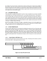
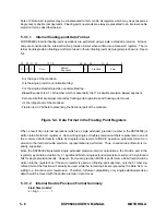
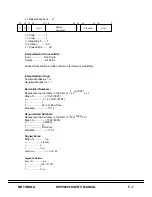
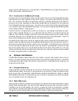
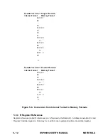
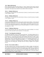
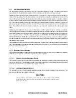
Figure 4-6. Operating Mode Register Format
4.11.3
Underflow flag (UF) Bit 5
The Underflow flag (UF) is set when a stack underflow occurs. The UF flag is cleared when a stack overflow
occurs. While the SE flag remains set, the UF flag does not change with Stack Pointer operations caused
by instructions that refer implicitly to the Stack Pointer such as RTI, RTS, DO, ENDDO, JSR, etc. The UF
flag is cleared by hardware reset (see Figure 4-5). Implicit stack pointer operations that do not produce a
stack error (i.e. do not set SE) will always clear UF as long as SE is not set.
4.11.4
Unimplemented Stack Pointer Register bits (Bits 6-31)
Any unimplemented stack pointer register bits are reserved for future expansion and read as zero during
DSP96002 read operations. They should be written with zero for future compatibility.
4.12
OPERATING MODE REGISTER (OMR)
The operating mode register (OMR) is a 32-bit register which defines the current chip operating mode of the
processor. The OMR bits are only affected by processor reset and by instructions which directly reference
the OMR.
The operating mode register format is shown in Figure 4-6 and is described below.
4.12.1
Chip Operating Mode (Bits 0,1,2)
The operating mode bits MA, MB and MC determine if the internal program RAM is enabled and the startup
procedure when the chip leaves the RESET state. These bits are loaded from the external Mode Select pins
MODC, MODB and MODA respectively when the
—
R
—
E
—
S
—
E
–
T pin is negated. After the DSP96002
leaves the RESET state, MC, MB and MA may be changed under program control. See Section 9 for more
details on the chip operating modes.
4.12.2
Data ROM Enable (Bit 3)
The Data ROM Enable (DE) bit enables the two on-chip 512x32 Data ROMs located at address $00000400
to $000007FF in the X and Y memory spaces. When DE is cleared, the $00000200 to $000007FF space is
part of the external X and Y data spaces and the on-chip Data ROMs are disabled (see the DSP96002 data
memory maps in Section 9.2 for additional details).
4.12.3
Reserved Operating Mode Register (Bits 4-31)
These operating mode register bits are reserved for future expansion and will read as zero during
DSP96002 read operations. They should be written with zero for future compatibility.
31
4
3
2
1
0
Operating Mode
Data Rom Enable
Reserved
*
DE
MC
MB
MA
Содержание DSP96002
Страница 3: ...1 2 DSP96002 USER S MANUAL MOTOROLA ...
Страница 38: ...MOTOROLA DSP96002 USER S MANUAL 3 15 Figure 3 4 Modulo Arithmetic Unit Block Diagram ...
Страница 39: ...3 16 DSP96002 USER S MANUAL MOTOROLA ...
Страница 53: ...4 14 DSP96002 USER S MANUAL MOTOROLA ...
Страница 76: ...MOTOROLA DSP96002 USER S MANUAL 5 23 Figure 5 8 Address Modifier Summary ...
Страница 86: ...6 10 DSP96002 USER S MANUAL MOTOROLA ...
Страница 101: ...MOTOROLA DSP96002 USER S MANUAL 7 15 Figure 7 9 HI Block Diagram One Port ...
Страница 140: ...7 54 DSP96002 USER S MANUAL MOTOROLA ...
Страница 166: ...9 10 DSP96002 USER S MANUAL MOTOROLA ...
Страница 181: ...MOTOROLA DSP96002 USER S MANUAL 10 15 Figure 10 8 Program Address Bus FIFO ...
Страница 336: ...A 148 DSP96002 USER S MANUAL MOTOROLA FMPY S2 S1 D1 FSUB S S3 D2 move syntax see the MOVE instruction de scription ...
Страница 337: ...MOTOROLA DSP96002 USER S MANUAL A 149 ...
Страница 404: ...A 216 DSP96002 USER S MANUAL MOTOROLA PC xxxx D ...
Страница 460: ...A 272 DSP96002 USER S MANUAL MOTOROLA SIOP Not affected ...
Страница 484: ...A 296 DSP96002 USER S MANUAL MOTOROLA SSH PC SSL SR SP 1 SP ...
Страница 519: ...MOTOROLA DSP96002 USER S MANUAL A 331 ...
Страница 580: ...MOTOROLA DSP96002 USER S MANUAL B 61 X Memory Y Memory n0 3 r0 x0 Xmin r4 y0 Xmax z0 Ymin x1 Ymax y1 Zmin z1 Zmax ...
Страница 718: ...MOTOROLA DSP96002 USER S MANUAL B 199 ...
Страница 871: ... MOTOROLA INC 1994 MOTOROLA TECHNICAL DATA SEMICONDUCTOR M Addendum ...
Страница 888: ...MOTOROLA INDEX 1 INDEX ...
Страница 889: ......


