


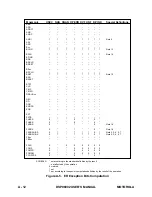

MOTOROLA
DSP96002 USER’S MANUAL
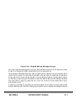
10 - 21
(ODEC releases the chip from the "halt" state and the instruction is executed again (in a "RE-
PEAT-like" fashion. The signal that marks the end of the instruction returns the chip to the
"halt" state and an acknowledge is issued to the command controller.)
24.
ACK
25.
Send command READ GDB REGISTER
(ODEC selects GDB as source for serial data and an acknowledge is issued to the command
controller.)
26.
ACK
27.
CLK
28.
Repeat from step 23 until the entire memory area is examined. At the end of the process R0
has to be restored.
10.12.4
Returning from Debug Mode to Normal Mode
There are two cases for returning from the debug mode. Either control will be returned to the program that
was running before debug was initiated or the registers will be changed to jump to a different program.
10.12.4.1
Case 1: Return to the previous program (Return to normal mode).
1.
Send command WRITE PDB REGISTER (no GO, no EX).
(ODEC selects the PDB as the destination for serial data – also, ODEC selects the on-chip
PAB register as the source for the PAB bus. After the PAB was driven, an acknowledge is is-
sued to the command controller.)
2.
ACK
3.
Send the 32 bits of the saved PIL (instruction latch) value.
(After all the 32-bits have been received the PDB register drives the PDB. ODEC causes the
core to load the opcode. An acknowledge is issued to the command controller.)
4.
ACK
5.
Send command WRITE PDB REGISTER (GO, EX).
(ODEC selects PDB as destination for serial data.)
6.
ACK
7.
Send the 32-bit of the saved PDB value.
(After 32 bits have been received, the PDB register drives the PDB. ODEC releases the chip
from the "halt" state and the Debug Mode bit in OSCR is cleared. The chip continues to ex-
ecute instructions until a Debug Mode condition occurs.)
10.12.4.2
Case 2: Jump to a new program (Go from address $xxxxxxxx).
1.
Send command WRITE PDB REGISTER (no GO, no EX).
(ODEC selects PDB as destination for serial data.)
2.
ACK
3.
Send 32 bits of the opcode of a two word jump instruction ($030c3f80) instead of the saved
PIL (instruction latch) value.
(After all the 32-bits have been received the PDB register drives the PDB. ODEC causes the
core to load the opcode. An acknowledge is issued to the command controller.)
Содержание DSP96002
Страница 3: ...1 2 DSP96002 USER S MANUAL MOTOROLA ...
Страница 38: ...MOTOROLA DSP96002 USER S MANUAL 3 15 Figure 3 4 Modulo Arithmetic Unit Block Diagram ...
Страница 39: ...3 16 DSP96002 USER S MANUAL MOTOROLA ...
Страница 53: ...4 14 DSP96002 USER S MANUAL MOTOROLA ...
Страница 76: ...MOTOROLA DSP96002 USER S MANUAL 5 23 Figure 5 8 Address Modifier Summary ...
Страница 86: ...6 10 DSP96002 USER S MANUAL MOTOROLA ...
Страница 101: ...MOTOROLA DSP96002 USER S MANUAL 7 15 Figure 7 9 HI Block Diagram One Port ...
Страница 140: ...7 54 DSP96002 USER S MANUAL MOTOROLA ...
Страница 166: ...9 10 DSP96002 USER S MANUAL MOTOROLA ...
Страница 181: ...MOTOROLA DSP96002 USER S MANUAL 10 15 Figure 10 8 Program Address Bus FIFO ...
Страница 336: ...A 148 DSP96002 USER S MANUAL MOTOROLA FMPY S2 S1 D1 FSUB S S3 D2 move syntax see the MOVE instruction de scription ...
Страница 337: ...MOTOROLA DSP96002 USER S MANUAL A 149 ...
Страница 404: ...A 216 DSP96002 USER S MANUAL MOTOROLA PC xxxx D ...
Страница 460: ...A 272 DSP96002 USER S MANUAL MOTOROLA SIOP Not affected ...
Страница 484: ...A 296 DSP96002 USER S MANUAL MOTOROLA SSH PC SSL SR SP 1 SP ...
Страница 519: ...MOTOROLA DSP96002 USER S MANUAL A 331 ...
Страница 580: ...MOTOROLA DSP96002 USER S MANUAL B 61 X Memory Y Memory n0 3 r0 x0 Xmin r4 y0 Xmax z0 Ymin x1 Ymax y1 Zmin z1 Zmax ...
Страница 718: ...MOTOROLA DSP96002 USER S MANUAL B 199 ...
Страница 871: ... MOTOROLA INC 1994 MOTOROLA TECHNICAL DATA SEMICONDUCTOR M Addendum ...
Страница 888: ...MOTOROLA INDEX 1 INDEX ...
Страница 889: ......


