Enhanced Serial Audio Interface (ESAI)
GPIO - Pins and Registers
MOTOROLA
DSP56367
10-53
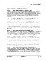
When programmed as input flags, the SCKR, FSR and HCKR logic values, respectively, are
latched at the same time as the first bit of the receive data word is sampled. Because the input
was latched, the signal on the input flag pin (SCKR, FSR or HCKR) can change without
affecting the input flag until the first bit of the next receive data word. When the received data
words are transferred to the receive data registers, the input flag latched values are then
transferred to the IF0, IF1 and IF2 bits in the SAISR register, where they may be read by
software.
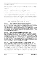
When programmed as output flags, the SCKR, FSR and HCKR logic values are driven by the
contents of the OF0, OF1 and OF2 bits in the SAICR register respectively, and are driven
when the transmit data registers are transferred to the transmit shift registers. The value on
SCKR, FSR and HCKR is stable from the time the first bit of the transmit data word is
transmitted until the first bit of the next transmit data word is transmitted. Software may
change the OF0-OF2 values thus controlling the SCKR, FSR and HCKR pin values for each
transmitted word. The normal sequence for setting output flags when transmitting data is as
follows: wait for TDE (transmitter empty) to be set, first write the flags, and then write the
transmit data to the transmit registers. OF0, OF1 and OF2 are double buffered so that the flag
states appear on the pins when the transmit data is transferred to the transmit shift register
(i.e., the flags are synchronous with the data).
10.5
GPIO - PINS AND REGISTERS
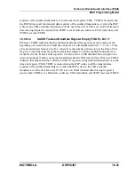
The GPIO functionality of the ESAI port is controlled by three registers: Port C control
register (PCRC), Port C direction register (PRRC) and Port C data register (PDRC).
10.5.1
PORT C CONTROL REGISTER (PCRC)
The read/write 24-bit Port C Control Register (PCRC) in conjunction with the Port C
Direction Register (PRRC) controls the functionality of the ESAI GPIO pins. Each of the
PC(11:0) bits controls the functionality of the corresponding port pin. See Table 10-12 for the
port pin configurations. Hardware and software reset clear all PCRC bits.
Содержание DSP56367
Страница 16: ...xvi MOTOROLA CONTENTS Paragraph Number Title Page Number ...
Страница 22: ...xxii MOTOROLA List of Figures Figure Number Title Page Number ...
Страница 26: ...xxvi MOTOROLA List of Tables Table Number Title Page Number ...
Страница 148: ...4 6 DSP56367 MOTOROLA Design Considerations PLL Performance Issues ...
Страница 248: ...9 30 DSP56367 MOTOROLA Serial Host Interface SHI Programming Considerations ...
Страница 306: ...10 58 DSP56367 MOTOROLA Enhanced Serial Audio Interface ESAI ESAI Initialization Examples ...
Страница 389: ...Bootstrap ROM Contents MOTOROLA DSP56367 A 15 end ...
Страница 390: ...A 16 DSP56367 MOTOROLA Bootstrap ROM Contents ...
Страница 432: ...C 8 DSP56367 MOTOROLA JTAG BSDL ...
Страница 484: ...D 52 DSP56367 MOTOROLA Programmer s Reference ...
Страница 490: ...E 6 DSP56367 MOTOROLA Power Consumption Benchmark ...
Страница 516: ...F 26 DSP56367 MOTOROLA IBIS Model ...
Страница 522: ...Index 6 MOTOROLA Index ...
Страница 523: ......


