10-16
DSP56367
MOTOROLA
Enhanced Serial Audio Interface (ESAI)
ESAI Programming Model
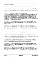
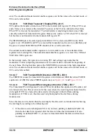
In the network mode, the operation of clearing TE0 and setting it again disables the
transmitter #0 after completing transmission of the current data word until the beginning of
the next frame. During that time period, the SDO0 pin remains in the high-impedance
state.The on-demand mode transmit enable sequence can be the same as the normal mode, or
TE0 can be left enabled.
10.3.2.2
TCR ESAI Transmit 1 Enable (TE1) - Bit 1
TE1 enables the transfer of data from TX1 to the transmit shift register #1. When TE1 is set
and a frame sync is detected, the transmit #1 portion of the ESAI is enabled for that frame.
When TE1 is cleared, the transmitter #1 is disabled after completing transmission of data
currently in the ESAI transmit shift register. The SDO1 output is tri-stated, and any data
present in TX1 is not transmitted (i.e., data can be written to TX1 with TE1 cleared; but data is
not transferred to the transmit shift register #1).
The normal mode transmit enable sequence is to write data to one or more transmit data
registers before setting TEx. The normal transmit disable sequence is to clear TEx, TIE and
TEIE after TDE equals one.
In the network mode, the operation of clearing TE1 and setting it again disables the
transmitter #1 after completing transmission of the current data word until the beginning of
the next frame. During that time period, the SDO1 pin remains in the high-impedance state.
The on-demand mode transmit enable sequence can be the same as the normal mode, or TE1
can be left enabled.
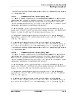
10.3.2.3
TCR ESAI Transmit 2 Enable (TE2) - Bit 2
TE2 enables the transfer of data from TX2 to the transmit shift register #2. When TE2 is set
and a frame sync is detected, the transmit #2 portion of the ESAI is enabled for that frame.
When TE2 is cleared, the transmitter #2 is disabled after completing transmission of data
currently in the ESAI transmit shift register. Data can be written to TX2 when TE2 is cleared
but the data is not transferred to the transmit shift register #2.
The SDO2/SDI3 pin is the data input pin for RX3 if TE2 is cleared and RE3 in the RCR
register is set. If both RE3 and TE2 are cleared the transmitter and receiver are disabled, and
the pin is tri-stated. Both RE3 and TE2 should not be set at the same time.
The normal mode transmit enable sequence is to write data to one or more transmit data
registers before setting TEx. The normal transmit disable sequence is to clear TEx, TIE and
TEIE after TDE equals one.
In the network mode, the operation of clearing TE2 and setting it again disables the
transmitter #2 after completing transmission of the current data word until the beginning of
the next frame. During that time period, the SDO2/SDI3 pin remains in the high-impedance
Содержание DSP56367
Страница 16: ...xvi MOTOROLA CONTENTS Paragraph Number Title Page Number ...
Страница 22: ...xxii MOTOROLA List of Figures Figure Number Title Page Number ...
Страница 26: ...xxvi MOTOROLA List of Tables Table Number Title Page Number ...
Страница 148: ...4 6 DSP56367 MOTOROLA Design Considerations PLL Performance Issues ...
Страница 248: ...9 30 DSP56367 MOTOROLA Serial Host Interface SHI Programming Considerations ...
Страница 306: ...10 58 DSP56367 MOTOROLA Enhanced Serial Audio Interface ESAI ESAI Initialization Examples ...
Страница 389: ...Bootstrap ROM Contents MOTOROLA DSP56367 A 15 end ...
Страница 390: ...A 16 DSP56367 MOTOROLA Bootstrap ROM Contents ...
Страница 432: ...C 8 DSP56367 MOTOROLA JTAG BSDL ...
Страница 484: ...D 52 DSP56367 MOTOROLA Programmer s Reference ...
Страница 490: ...E 6 DSP56367 MOTOROLA Power Consumption Benchmark ...
Страница 516: ...F 26 DSP56367 MOTOROLA IBIS Model ...
Страница 522: ...Index 6 MOTOROLA Index ...
Страница 523: ......


