background image

7I76   35

REFERENCE INFORMATION

SSLBP

NORMAL MODE OPERATION

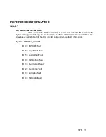
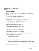
In normal mode the sequence of operations for a cyclic access with write before

read is as follows:

Note steps 1 through 5 are setup operations and are only done once per session

1. Issue STOP ALL command (0x800), wait for COMMAND register clear to verify stop
command completion.

2. Issue normal START command (0x9NN) with bitmask (NN) of channels to start.

3. Wait for COMMAND register clear to verify start command completion. (may be many
mS)

4.  Read  data  register  to  verify  that  all  selected  channels  started  (a  1  in  any  channel
position bit means a fault in the channel that the bit represents)

5. Read device unit number (This can only be read before DOIT has been asserted)

6. Check command register, if not clear, cycle time is too short. 

(Note the command register should never be written to when not clear except to issue a
stop command or when written with the command ignore bit set)

7.  Check  data  register,  any  1  bits  indicate  previous  DOIT  command  failed  for  in  the
corresponding channels

8. Read per channel Interface register 0 and interface register 1 for input process data

9. Write per channel output process data ( for 7I76) to interface 0 register and interface 1
register

10.  Write  DOIT  command  =  0x10NN  where  NN  is  the  bit  mask  of  channels  to  initiate
transfers.

11. Wait for next cycle,  at next cycle time, loop back to state 6

This sequence can be modified if a read-modify-write sequence is required, this

requires  polling  the  command  register  for  send/receive  completion.  This  will  take  a
maximum of 100 uSec from the DOIT command to command register clear and valid input
data.

Содержание 7I76

Страница 1: ...7I76 STEP DIR PLUS I O DAUGHTERCARD V1 22 ...

Страница 2: ......

Страница 3: ...S AND DEFAULT JUMPER POSITIONS 3 HOST INTERFACE CONNECTOR 4 TB2 STEP AND DIR CONNECTOR 5 TB3 STEP DIR ENCODER AND RS 422 CONNECTOR 6 TB4 SPINDLE CONNECTOR 7 FIELD INPUT OUTPUT CONNECTORS 8 TB6 PINOUT 8 TB5 PINOUT 9 FIELD POWER CONNECTOR 10 OPERATION 11 HOST INTERFACE 11 STEP DIR INTERFACE 11 RS 422 INTERFACE 11 ENCODER INTERFACE 12 SPINDLE INTERFACE 12 SPINDLE ISOLATED OUTPUTS 12 STATUS LEDS 12 ...

Страница 4: ...3 OVERTEMPERATURE PROTECTION 13 MAXIMUM PER CHIP CURRENT 14 VOLTAGE CLAMPS 14 FIELD INPUT CHARACTERISTICS 14 WHY SINKING INPUTS 14 ANALOG INPUTS 14 FIELD VOLTAGE MONITORING 14 WATCHDOG AND FAULTS 15 FIELD I O PARAMETERS 15 NON VOLATILE FIELD I O PARAMETERS 16 OPERATE MODE BAUD RATE 16 WATCHDOG TIMEOUT 16 RPD WPD AND UFLBP 17 SOFTWARE PROCESS DATA MODES 18 ...

Страница 5: ...NTERFACE AND CS REGISTER CONTENTS AT START 25 CS REGISTER AFTER START 27 CS REGISTER AFTER DOIT 27 PROCESS DATA DISCOVERY 28 PROCESS TABLE OF CONTENTS 28 PROCESS DATA DESCRIPTOR 29 PROCESS DATA DESCRIPTOR FIELDS 29 RECORD_TYPE 29 DATA_LENGTH 29 DATA_TYPE 30 DATA_DIRECTION 30 PARAMETER_MIN 30 PARAMETER_MAX 30 UNIT_STRING 31 NAME_STRING 31 NUMERIC PROCESS DATA SCALING 31 MODE DESCRIPTOR 31 MODE TYPE...

Страница 6: ...P DATA READ WRITEWCOMMAND 41 EXAMPLE COMMANDS 42 LOCAL LBP COMMANDS 43 LOCAL LBP READ COMMANDS 43 LOCAL LBP WRITE COMMANDS 45 RPC COMMANDS 45 EXAMPLE RPC COMMAND LIST 47 SPECIAL RPCS 48 CRC 48 FRAMING 48 SSERIAL REMOTE RPCS 49 SPECIFICATIONS 50 DRAWINGS 52 ...

Страница 7: ...voltage with direction and enable outputs is provided for spindle control as is a single spindle encoder channel with TTL or differential inputs 48 points of isolated field I O are provided for general control use including limit switch and control panel inputs coolant enable and tool changer control outputs Isolated I O includes 32 sinking inputs and 16 sourcing outputs Inputs can sense 5V to 32V...

Страница 8: ...osition 5V power must be supplied to the 7I76 via TB3 This option must be set to match the cable power option of the host FPGA card If the FPGA card supplies 5V W2 must be in the left hand position If the FPGA card does not supply 5V W2 must be in the right hand position Never apply external 5V power to the 7I76 s TB3 connector when W2 is in the left hand position or you may damage the 7I76 FPGA c...

Страница 9: ...7I76 3 CONNECTORS 7I76 CONNECTOR LOCATIONS AND DEFAULT JUMPER POSITIONS ...

Страница 10: ...9 STEP4 OUT 19 GND 7 IO10 SS0TX OUT 20 GND 8 IO11 SS0RX IN 21 GND 9 IO12 SS1TX OUT 22 GND or 5V 10 IO13 SS1RX IN 23 GND or 5V 11 IO14 ENCI IN 24 GND or 5V 12 IO15 ENCB IN 25 GND or 5V 13 IO16 ENCA IN Notes 1 If jumper W2 is is the left hand position pins 22 through 25 are 5V if W2 is in the right hand position Pins 22 through 25 are GND 2 GPIO pins are for first FPGA connector next connector serie...

Страница 11: ...ins TB2 is a 3 5 MM pluggable terminal block with supplied removable screw terminal plugs TB2 CONNECTOR PINOUT TB2 PIN SIGNAL TB2 PIN SIGNAL 1 GND 13 GND 2 STEP0 14 STEP2 3 STEP0 15 STEP2 4 DIR0 16 DIR2 5 DIR0 17 DIR2 6 5VP 18 5VP 7 GND 19 GND 8 STEP1 20 STEP3 9 STEP1 21 STEP3 10 DIR1 22 DIR3 11 DIR1 23 DIR3 12 5VP 24 5VP Note 5VP pins are PTC short circuit protected 5V output pins for field wirin...

Страница 12: ...gable terminal block with supplied removable screw terminal plugs TB3 CONNECTOR PINOUT TB3 PIN SIGNAL TB3 PIN SIGNAL 1 GND 13 IDX 2 STEP4 14 IDX 3 STEP4 15 GND 4 DIR4 16 RS 422 RX 5 DIR4 17 RS 422 RX 6 5VP 18 RS 422 TX 7 ENCA 19 RS 422 TX 8 ENCA 20 5VP 9 GND 21 5V 5V supply power 10 ENCB 22 5V 5V supply power 11 ENCB 23 GND 12 5VP 24 GND Note 5VP pins are PTC short circuit protected 5V output pins...

Страница 13: ...solated analog output and control signals for a spindle interface TB4 is a 8 terminal 3 5 MM pluggable terminal block with supplied removable screw terminal plugs TB4 PINOUT TB4 PIN SIGNAL 1 SPINDLE 2 SPINDLE OUT 3 SPINDLE 4 NC 5 SPINDLE ENA 6 SPINDLE ENA 7 SPINDLE DIR 8 SPINDLE DIR ...

Страница 14: ...minated at TB5 TB6 and TB5 are 3 5 MM pluggable terminal block with supplied removable screw terminal plugs Pin one is at the bottom edge of the 7I76 card TB6 CONNECTOR PINOUT TB6 PIN I O TB6 PIN I O 1 INPUT0 13 INPUT12 2 INPUT1 14 INPUT13 3 INPUT2 15 INPUT14 4 INPUT3 16 INPUT15 5 INPUT4 17 OUTPUT0 6 INPUT5 18 OUTPUT1 7 INPUT6 19 OUTPUT2 8 INPUT7 20 OUTPUT3 9 INPUT8 21 OUTPUT4 10 INPUT9 22 OUTPUT5...

Страница 15: ...TPUT TB5 PIN OUTPUT 1 INPUT16 13 INPUT28 2 INPUT17 14 INPUT29 3 INPUT18 15 INPUT30 4 INPUT19 16 INPUT31 5 INPUT20 17 OUTPUT8 6 INPUT21 18 OUTPUT9 7 INPUT22 19 OUTPUT10 8 INPUT23 20 OUTPUT11 9 INPUT24 21 OUTPUT12 10 INPUT25 22 OUTPUT13 11 INPUT26 23 OUTPUT14 12 INPUT27 24 OUTPUT15 ...

Страница 16: ...1 VFIELD FIELD POWER 8 32V Bottom pin 2 VFIELD FIELD POWER 8 32V 3 VFIELD FIELD POWER 8 32V 4 VFIELD FIELD POWER 8 32V 5 VIN LOGIC POWER 8 32V 6 NC 7 NC 8 GROUND VIN VFIELD COMMON Top pin Note When W1 is in the default left hand position VIN is connected to VFIELD so only VFIELD need be supplied to the 7I76 to power its field IO ...

Страница 17: ... with the unused signals left unconnected at the 7I76 The input common signal on drives with single ended inputs connects to the 7I76s GND or 5VP pins depending on the drive type RS 422 INTERFACE The 7I76 has one RS 422 interface available on TB3 This interface is intended for I O expansion with Mesa SSERIAL devices The easiest way to make a cable for interfacing the 7I76 to these devices is to ta...

Страница 18: ...een 5VDC an 15VDC with SPINDLE always being more positive than SPINDLE Because the analog output is isolated bipolar output is possible for example with SPINDLE connected to 5V and SPINDLE connected to 5V a 5V analog output range is created In this case the spindle output must be offset so that 50 of full scale is output when a 0V output is required Note that if bipolar output is used the output w...

Страница 19: ... or too low will cause faults FIELD OUTPUT CHARACTERISTICS The 7I76 field outputs are high side or sourcing type MOSFET drivers that is they source positive voltage to a ground referred load For example with a standard 24V field power 24V connects to the 7I76s field power input on TB1 and the outputs on TB5 and TB6 now source 24V power to loads All 7I76 loads will have one side returned to ground ...

Страница 20: ...40 of 24V 9 6V to be sensed as low These accurate thresholds and hysteresis allow high speed field signal detection while maintaining excellent noise immunity WHY SINKING INPUTS 7I76 field inputs are of the sinking type That is external power must be applied to the input to register as activated This mode was chosen so that accidental grounding of an input will not register as an activated input I...

Страница 21: ...the 7I76s startup condition meaning the host must first clear the fault before starting normal operation This is normally handled by SSLBP FIELD I O PARAMETERS The 7I76 has several user settable parameters but normally only a very few need be changed in normal operation PARAMETER TYPE FUNCTION NVBAUDRATE UINT Sets operate mode baudrate NVUNITNUMBER ULONG Non volatile unit number UNITNUMBER ULONG W...

Страница 22: ...ATE parameter The index numbers for available baud rates are as follows INDEX BAUD INDEX BAUD INDEX BAUD 0 9600B 1 19200B 2 38400B 3 57600B 4 115200B 5 230400B 6 460800B 7 921600B 8 1 25MB 9 2 5MB 10 5MB 11 10MB WATCHDOG TIMEOUT The default watchdog period is 50 mS but can be set to different periods to suit the application Watchdog timeout units are mS A watchdog timeout value of 0 will disable t...

Страница 23: ...lowing environment variables should be set SET BAUDRATE 115200 SET BAUDRATEMUL 1 SET PROTOCOL LBP SET INTERFACE OSDEVICE Example setting NVWATCHDOGTIMEOUT to 100 ms WPD NVWATCHDOGTIME 100 Note this is permanent change in the 7I76s watchdog timeout and like all non volatile parameters will only be applied after the 7I76 has been power cycled Example reading 7I76 faults in Hexadecimal RPD FAULT H Ex...

Страница 24: ...esulting in higher maximum update rates MODE 0 I O only mode 32 bits of input data 16 bit of output data MODE 1 I O plus analog input mode 32 bits of input data 16 bits of output data 4 analog input channels MODE 2 I O plus analog input and field voltage and MPG mode 32 bits of input data 16 bits of output data 4 analog input channels field voltage analog in and 2 MPG encoders on inputs 16 19 Defa...

Страница 25: ...I76 SSERIAL is a part of the HostMot2 motion interface firmware for MESA s Anything I O FPGA cards REGISTER MAP SSLBP has two global processor interface registers and four per channel remote device interface registers For more details on mapping of these registers in HostMot2 memory space see the REGMAP file that is included with the HostMot2 source distribution PROCESSOR INTERFACE REGISTERS There...

Страница 26: ...e device A set bit indicates that the corresponding channel will start or do a data transfer A command is started when written to the command register Command completion is signaled by the command register being cleared to 0x0000 by the internal SSLBP firmware If the command register is read before the command is complete it will reflect the previously written command The command register should n...

Страница 27: ...he parameter address ORed with the Request bit bit 13 is written to the command register 2 The host polls the command register until it reads as zero 3 The host reads the parameter byte from the data register LOCAL WRITE OPERATIONS The sequence used for writing a local SSLBP variable is as follows 1 The host polls the command register until it reads as zero 2 The host writes the data byte to the d...

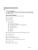
Страница 28: ... LOCAL PARAMETER ADDRESS DESCRIPTION INTERFACE_TYPE 0x0000 0x12 for SSLBP INTERFACE_WIDTH 0x0001 Data port width 8 MAJORREV 0x0002 Major SSLBP firmware revision MINORREV 0x0003 Minor SSLBP firmware revision GP_INPUTS 0x0004 Number of GP input bits 0 for SSLBP GP_OUTPUTS 0x0005 Number of GP output bits 0 for SSLBP PROCESSOR_TYPE 0x0006 0xD8 for Dumb8 CHANNELS 0x0007 1 to 8 depending on configuratio...

Страница 29: ...ote device This setup includes clearing any faults setting remote operational mode and setting the outputs off If no errors have occurred and all faults are clearable the SSLBP firmware enters a chatter loop where it repeatedly sends output data of all 0 s This keeps the remote devices watchdog fed while waiting for the first DOIT command When the command completes the command register is clear th...

Страница 30: ...ata from the interface registers to the remote device and request data from the remote device for presentation in the interface registers to the host This SSLBP function is designed for high speed real time operation Synchronization with the host is accomplished with the DOIT command When the host writes a DOIT command all outgoing process data from the host is sent to the remote devices and incom...

Страница 31: ...o the most significant byte of the remote channels CSR before a START or SETUP START command is issued A default value of 0x00000000 should be written to all CSRs if MODE is not used REMOTE MODE IS WRITTEN TO CSR MS BYTE BEFORE START CS REG MODE 0 0 0 INTERFACE AND CS REGISTER DATA AT START After a successful start command either setup start or normal start Interface register 0 reports the remote ...

Страница 32: ...the following format Byte3 X undefined for SSLBP versions 29 remote fault for versions 28 See CS REGISTER AFTER DOIT section Byte2 COM_STATE Communication state code debug only Byte1 Communication status code 0x00 for OK Bit 7 CommunicationNotReady Bit 6 NoRemoteID Bit 5 CommunicationError Bit 0 RemoteFault Byte0 Local Communication faults sticky cleared only by STOP Bit 7 TooManyerrors Bit 6 Remo...

Страница 33: ...h 2 of CS register are the same as after a start command but in addition the previously invalid byte 3 of the CS register contains remote fault information Byte3 REMOTE_FAULTS Bit 7 LBPCOMFault Bit 6 IllegalMode Fault Bit 5 LowVoltageFault Bit 4 HighVoltageFault Bit 3 OverCurrentFault Bit 2 OverTempFault Bit 1 NoEnableFault Bit 0 WatchdogFault ...

Страница 34: ...built in knowledge of the remote device PROCESS TABLE OF CONTENTS After a normal start or setup start command the PTOCP word in the low word of interface register 2 is a pointer to the current process table of contents PTOC in the remote device If remote devices that do not support process device discovery are present their PTOCP will be 0 and process data organization must be inferred from the re...

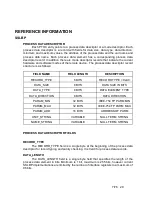
Страница 35: ...CRIPTION RECORD_TYPE 8 BITS RECORD TYPE 0xA0 DATA_SIZE 8 BITS DATA SIZE IN BITS DATA_TYPE 8 BITS DATA ELEMENT TYPE DATA_DIRECTION 8 BITS DATA DIRECTION PARAM_MIN 32 BITS IEEE 754 FP PARM MIN PARAM_MAX 32 BITS IEEE 754 FP PARM MAX PARAM_ADD 16 BITS ADDRESS OF PARM UNIT_STRING VARIABLE NULL TERM STRING NAME_STRING VARIABLE NULL TERM STRING PROCESS DATA DESCRIPTOR FIELDS RECORD_TYPE The RECORD_TYPE f...

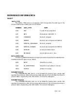
Страница 36: ...The DATA_DIRECTION field is a single byte field that specifies the data direction Valid Data direction bytes are as follows 0x00 INPUT Read from remote 0x40 BI_DIRECTIONAL Read from and written to remote 0X80 OUTPUT Written to remote PARAMETER_MIN The PARAMETER_MIN field is a 32 bit IEEE 754 floating point number that specifies the minimum value of the process data element This is to allow the dri...

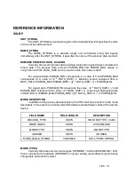
Страница 37: ...f 2 DATA_SIZE 1 Meaning scaled unsigned data is RAW_DATA PARAM_MAX PARAM_MIN 2 DATA_SIZE 1 PARAM_MIN For signed data PARAM_MIN corresponds the value 2 DATA_SIZE 1 1 and PARAM_MAX corresponds the value 2 DATA_SIZE 1 1 meaning scaled signed data is RAW_DATA PARAM_MAX PARAM_MIN 2 DATA_SIZE 1 1 PARAM_MIN MODE DESCRIPTOR In addition to the process data descriptors the PTOC will have pointers to two mod...

Страница 38: ...d from interface register 0 through interface register 2 Read data and bidirectional data is unpacked from the interface registers read by the host Write data and bidirectional data is packed into the interface registers written by the host Before a DOIT command is written to start a data transfer cycle with the remote device the host must write its packed outgoing process data OPD in table below ...

Страница 39: ...OST READS INCOMING INTERFACE REGISTERS AFTER DOIT CS REG REMOTE FLT COM_STATE STATUS LOCAL FLT INTERFACE 0 IPD BYTE 3 IPD BYTE 2 IPD BYTE 1 IPD BYTE 0 INTERFACE 1 IPD BYTE 7 IPD BYTE 6 IPD BYTE 5 IPD BYTE 4 INTERFACE 2 IPD BYTE 11 IPD BYTE 10 IPD BYTE 9 IPD BYTE 8 7I76 SPECIFIC PROCESS DATA EXAMPLE Process data is remote device dependent and also dependent on remote device mode The 7I76 supports 3...

Страница 40: ...OUT 7 0 TB5 OUTS 15 8 TB6 OUTS 7 0 INTERFACE 1 X X SPINDIR SPINENA INTERFACE 2 X X X X 7I76 INCOMING PROCESS DATA FOR MODE 1 CS REG REMOTE FLT COM_STATE STATUS LOCAL FLT INTERFACE 0 TB5 INS 31 24 TB5 INS 23 16 TB6 INS 15 8 TB6 INS 7 0 INTERFACE 1 ANALOG3 ANALOG2 ANALOG1 ANALOG0 INTERFACE 2 X X X X Note that this information is just for user convenience as the process data organization in the inter...

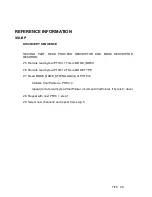
Страница 41: ...asserted 6 Check command register if not clear cycle time is too short Note the command register should never be written to when not clear except to issue a stop command or when written with the command ignore bit set 7 Check data register any 1 bits indicate previous DOIT command failed for in the corresponding channels 8 Read per channel Interface register 0 and interface register 1 for input pr...

Страница 42: ... READ EXAMPLE For a remote word read the sequence of operations is as follows 1 Issue a STOPALL command 0x800 wait for COMMAND register clear to verify stop command completion 2 Issue a setup START command 0xFNN with bitmask NN of channels to start 3 Wait for COMMAND register clear to verify start command completion may be many mS 4 Read data register to verify that all selected channels started a...

Страница 43: ...ult in the channel that the bit represents 5 Write the newparameter data to the selected channels Interface0 register right justified 6 Write LBP word write command 0x65 in the MSByte ORed with the parameter address to the selected channels CS register 0x6500PPPP 7 Issue a DOIT Command 8 Wait for the command register to be clear 9 Check that the data register is clear any set bits indicate an erro...

Страница 44: ...o verify stop command completion 2 Issue a setup START command 0xFNN with bitmask NN of channels to start 3 Wait for COMMAND register clear to verify start command completion may be many mS 4 Read data register to verify that the selected channels started a 1 bit means a fault in the channel that the bit represents 5 Read PTOCP from interface register 2 of selected channel if zero remote device do...

Страница 45: ...PTOC 1 This is DATA_SIZE 17 Remote read byte at PTOC 2 This is DATA_TYPE 18 Remote read byte at PTOC 3 This is DATA_DIRECTION 19 Remote read long at PTOC 4 This is PARAM_MIN 20 Remote read long at PTOC 8 This is PARAM_MAX 21 Remote read word at PTOC 10 This is PARAM_ADD not used normally 22 Read UNIT_STRING starting at PTOC 12 Initialize CharPointer to PTOC 12 repeat remote read byte at CharPointe...

Страница 46: ...mote read byte at PTOC 1 This is MODE_INDEX 26 Remote read byte at PTOC 2 This is MODE TYPE 27 Read MODE_NAME_STRING starting at PTOC 4 Initialize CharPointer to PTOC 4 repeat remote read byte at CharPointer increment CharPointer if byte is 0 done 28 Repeat with next PTOC step 1 29 Select next channel and repeat from step 5 ...

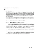
Страница 47: ...rd access as all the low level details are handed by the SSLBP code in the SSerial interface built into the FPGA but is presented here for completeness LBP DATA READ WRITE COMMAND 0 1 WR RID AI AS DS1 DS0 Bit 7 6 CommandType Must be 01b to specify data read write command Bit 5 Write 1 to specify write 0 to specify read Bit 4 RPCIncludesData 0 specifies that data is from stream 1 that data is from ...

Страница 48: ... Address MSB 0 0 0 0 0 0 0 0 Write data 0 1 0 1 0 1 0 1 0 Write Data 1 1 0 1 1 1 0 1 1 Write Data 2 1 1 0 0 1 1 0 0 Write Data 3 1 1 0 1 1 1 0 1 Write 2 more bytes 0xEE 0xFF at 0x014 and 0x015 COMMAND BITS CT1 CT0 WR RID AI AS DS1 DS0 LBPWrite 0 add 2 data 0 1 1 0 0 0 0 1 Write data 0 1 1 1 0 1 1 1 0 Write data 1 1 1 1 1 1 1 1 1 Read 8 bytes at 0x010 0x011 0x012 0x013 0x014 0x015 0x016 0x017 COMMA...

Страница 49: ...Get unit address 0xC1 Get LBP status LBP Status bit definitions BIT 7 Reserved BIT 6 Command Timeout Error BIT 5 Invalid write Error attempted write to protected area BIT 4 Buffer overflow error BIT 3 Watchdog timeout error BIT 2 Reserved BIT 1 Reserved BIT 0 CRC error 0xC2 Get CRC enable status note CRCs are always enabled on the 7I76 0xC3 Get CRC error count 0xC4 0xC9 Reserved 0xCA Get Enable_RP...

Страница 50: ...guration name only on some configurations 0xD8 Get low address 0xD9 Get high address 0xDA Get LBP version 0xDB Get LBP Unit ID Serial only not used with USB 0xDC Get RPC Pitch 0xDD Get RPC SizeL Low byte of RPCSize 0xDE Get RPC SizeH High byte of RPCSize 0xDF Get LBP cookie returns 0x5A ...

Страница 51: ...RC error count 0xE4 0xE9 Reserved 0xEA Set Enable_RPCMEM access flag non zero to enable access to RPC memory 0xEB Set Command timeout in mS for USB and character times for serial 0xEC 0xEF Reserved 0xF0 0xF6 Reserved 0xF7 Write LEDs 0xF8 Set low address 0xF9 Set high address 0xFA Add byte to current address 0xFB 0xFC Reserved 0xFD Set unit ID serial only 0xFE Reset LBP processor if followed by 0x5...

Страница 52: ...RPCNumber Specifies RPC 0 through 63 In the 7I76 LBP implementation RPCPitch is 0x8 bytes so each RPC command has native size of 0x08 bytes and start 0x8 byte boundaries in the RPC table area RPCs can cross RPCPitch boundaries if larger than RPCPitch RPCs are needed The stored RPC commands consist of LBP headers and addresses and possibly data if the command header has the RID bit set RPC command ...

Страница 53: ...bytes to address 0x10 0x11 with 2 data bytes supplied by host Command2 Reads two data bytes from address 0x12 0x13 COMMAND BITS CT1 CT0 WR RID I AS DS1 DS0 LBPWrite 2 add 2 data 0 1 1 0 0 1 0 1 Write Address LSB 0 0 0 1 0 0 0 0 Write Address MSB 0 0 0 0 0 0 0 0 LBPRead 2 add 2 data 0 1 0 0 0 1 0 1 Read Address LSB 0 0 0 1 0 0 1 0 Read Address MSB 0 0 0 0 0 0 0 0 Terminator 0 0 0 0 0 0 0 0 The data...

Страница 54: ...Cs with no reads will still cause a CRC byte to be returned this CRC byte will always be 00H FRAMING Since LBP is a binary protocol with no special sync characters the packet framing must be determined by other methods Framing is done by a combination of timing and pre parsing the serial data Timing based framing is used to reset the parser at gaps in the serial data stream This provides fast resy...

Страница 55: ...e following order RXSize TXSize PTOCLSB PTOCMSB GTOCLSB GTOCMSB RXSize is host relative so this is the size of data that the remote transmits Likewise TXSize is host relative so this is the size of process data the remote receives Note that the remote should check its remote SW mode and remote HW mode flags and return size data and pointers appropriate for the currently selected mode Note that the...

Страница 56: ...O LOGIC POWER 8VDC 32 VDC VIN POWER CONSUMPTION 1 W Typ 600 mW FIELD POWER 5VDC 28VDC FIELD OUTPUT CURRENT 350 mA Per output RESISTIVE LOADS AND INDUCTIVE LOADS WITH FLYBACK DIODE FIELD OUTPUT CURRENT 60 mA Per output INDUCTIVE LOADS WITH NO FLYBACK DIODE PER DRIVER CHIP CURRENT 1 4A Per chip HIGH SPEED ENCODER INPUT INPUT COMMON MODE RANGE 7 12 Volts INPUT TTL MODE THRESHOLD 1 4 1 8 Volts DIFFERE...

Страница 57: ...Volts OUTPUT HIGH 24 mA source VCC 8 Volts SPINDLE INTERFACE REFERENCE VOLTAGE 5 15 Volts SPINDLE B SPINDLE SUPPLY CURRENT 20 mA ISOLATION VOLTAGE 500 Volts DC NON LINEARITY 1 at 5KHz DIR ENA OUTPUT CURRENT 50 mA DIR ENA OUTPUT VOLTAGE 100 Volts DC DIR ENA ISOLATION VOLTAGE 500 Volts DC ENVIRONMENTAL TEMPERATURE C VERSION 0o C 70o C TEMPERATURE I VERSION 40o C 85o C ...

Страница 58: ...7I76 52 DRAWINGS ...

Отзывы: