background image

LTC3810-5

24

38105fd

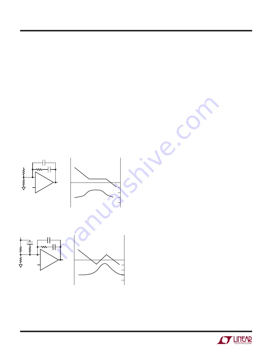
Figure 11. Type 2 Schematic and Transfer Function

requirement of the compensation will be to guarantee that 

the gain is below zero at frequencies above f

SW

/4. If the 

ESR zero is above the crossover frequency, the feedback 

amplifier will probably be required to provide phase boost. 

For most LTC3810-5 applications, Type 2 compensation will 

provide enough phase boost; however some applications 

where high bandwidth is required with low ESR ceramics 

and lots of bulk capacitance, Type 3 compensation may 

be necessary to provide additional phase boost.
The two types of compensation networks, “Type 2” and 

“Type 3” are shown in Figures 11 and 12. When compo-

nent values are chosen properly, these networks provide 

a “phase bump” at the crossover frequency. Type 2 uses 

a single pole-zero pair to provide up to about 60° of phase 

boost while Type 3 uses two poles and two zeros to provide 

up to 150° of phase boost.

Figure 12. Type 3 Schematic and Transfer Function

Feedback Component Selection
Selecting the R and C values for a typical Type 2 or Type 3 

loop is a nontrivial task. The applications shown in this 

data sheet show typical values, optimized for the power 

components shown. They should give acceptable perfor-

mance with similar power components, but can be way off if 

even one major power component is changed significantly. 

Applications that require optimized transient response will 

require recalculation of the compensation values specifically 

for the circuit in question. The underlying mathematics are 

complex, but the component values can be calculated in 

a straightforward manner if we know the gain and phase 

of the modulator at the crossover frequency.
Modulator gain and phase can be obtained in one of 

three ways: measured directly from a breadboard, or if 

the appropriate parasitic values are known, simulated or 

generated from the modulator transfer function. Mea-

surement will give more accurate results, but simulation 

or transfer function can often get close enough to give 

a working system. To measure the modulator gain and 

phase directly, wire up a breadboard with an LTC3810-5 

and the actual MOSFETs, inductor and input and output 

capacitors that the final design will use. This breadboard 

should use appropriate construction techniques for high 

speed analog circuitry: bypass capacitors located close 

to the LTC3810-5, no long wires connecting components, 

appropriately sized ground returns, etc. Wire the feedback 

amplifier with a 0.1µF feedback capacitor from I

TH

 to FB 

and a 10k to 100k resistor from V

OUT

 to FB. Choose the 

bias resistor (R

FB2

) as required to set the desired output 

voltage. Disconnect R

FB2

 from ground and connect it to 

a signal generator or to the source output of a network 

analyzer to inject a test signal into the loop. Measure the 

gain and phase from the I

TH

 pin to the output node at the 

positive terminal of the output capacitor. Make sure the 

analyzer’s input is AC coupled so that the DC voltages 

present at both the I

TH

 and V

OUT

 nodes don’t corrupt the 

measurements or damage the analyzer.
If breadboard measurement is not practical, a SPICE 

simulation can be used to generate approximate gain/

phase curves. Plug the expected capacitor, inductor and 

MOSFET values into the following SPICE deck and gener-

ate an AC plot of V

OUT

/V

ITH

 with gain in dB and phase in 

applicaTions inForMaTion

GAIN (dB)

38105 F11

0

PHASE

–6dB/OCT

–6dB/OCT

GAIN

PHASE (DEG)

FREQ

–90

–180

–270

–360

R

FB2

V

REF

R

FB1

R2

FB

C2

IN

OUT

+

C1

GAIN (dB)

38105 F12

0

PHASE

–6dB/OCT

+6dB/OCT

–6dB/OCT

GAIN

PHASE (DEG)

FREQ

–90

–180

–270

–360

V

REF

R2

FB

C2

IN

OUT

+

C1

C3

R3

R

FB2

R

FB1

Содержание LTC3810-5

Страница 1: ...ase Station Power Supplies n Networking Equipment Servers n Automotive and Industrial Control Systems n High Voltage Operation Up to 60V n Large 1 Gate Drivers n No Current Sense Resistor Required n D...

Страница 2: ...ODE SYNC ITH VFB PLL LPF SENSE NC NC NC SENSE BGRTN BG DRVCC NC I ON NC NC NC BOOST TG SW SS TRACK NC NC SHDN UVIN NDRV EXTV CC INTV CC TJMAX 125 C JA 34 C W EXPOSED PAD PIN 33 IS SGND MUST BE SOLDERE...

Страница 3: ...2 V ISHDN SHDN Pin Input Current 0 1 A VUVIN UVIN Undervoltage Lockout UVIN Rising UVIN Falling Hysteresis l l 0 86 0 78 0 07 0 89 0 80 0 10 0 92 0 82 0 12 V V V VVCCUV INTVCC Undervoltage Lockout Lin...

Страница 4: ...EXTVCC 6V VEXTVCC 15V 5 2 5 5 5 8 V DVEXTVCC 1 VEXTVCC VINTVCC at Dropout ICC 20mA VEXTVCC 5V 75 150 mV DVLOADREG 1 INTVCC Load Regulation from EXTVCC ICC 0mA to 20mA VEXTVCC 10V 0 01 VINTVCC 2 INTVCC...

Страница 5: ...RT 0 1 FRONT PAGE CIRCUIT 200 s DIV VOUT 5V DIV VFB 0 5V DIV IL 5A DIV 38105 G04 VIN 48V FRONT PAGE CIRCUIT 500 s DIV 38105 G05 VOUT 5V DIV SS TRACK 0 5V DIV VFB 0 5V DIV IL 5A DIV VIN 48V ILOAD 1A MO...

Страница 6: ...300 400 3 0 VRNG 2V 1 4V 1V 0 7V 0 5V ION CURRENT A 10 10 ON TIME ns 100 1000 10000 100 1000 10000 38105 G12 VON INTVCC VON VOLTAGE V 0 400 500 700 1 5 2 5 38105 G13 300 200 0 5 1 2 3 100 0 600 ON TI...

Страница 7: ...VINTVCC 5V 50 25 75 25 0 50 100 150 125 TEMPERATURE C R DS ON 1 25 1 50 1 75 38105 G20 1 00 0 75 0 50 0 25 VBOOST VINTVCC 5V DRVCC BOOST VOLTAGE V 4 5 7 9 11 13 PEAK SOURCE CURRENT A 3 0 2 5 2 0 1 5 1...

Страница 8: ...stics INTVCC VOLTAGE V 0 200 250 300 6 10 38105 G27 150 100 2 4 8 12 14 50 0 INTV CC CURRENT A 50 25 75 25 0 50 100 150 125 TEMPERATURE C SS TRACK CURRENT A 2 3 38105 G28 1 0 LOAD CURRENT A 0 2 0 3 0...

Страница 9: ...tage ranges from 0V to 2 6V with 1 2V corresponding to zero sense voltage zero current VFB Pin7 FeedbackInput ConnectVFBthrougharesistor divider network to VOUT to set the output voltage PLL LPF Pin 8...

Страница 10: ...resistor or MOSFET SW Pin 25 Switch Node Connection to Inductor and Bootstrap Capacitor The voltage swing at this pin is 0 7V a Schottky diode external voltage drop to VIN TG Pin 26 Top Gate Drive Th...

Страница 11: ...24 SW 25 TG BOOST CB 26 27 EXTVCC 15 INTVCC NDRV 16 14 UV 0 72V OV 0 88V CVCC VOUT M2 M1 M3 L1 COUT CIN SS TRACK DB 4 VIN VIN SENSE 20 OVERTEMP SENSE FOLDBACK 0 8V REF 5V REG INTVCC ITH 5 8 ION 31 VI...

Страница 12: ...behaves as a constant frequency part against the load and supply variations Pulling the SHDN pin low forces the controller into its shutdown state turning off both M1 and M2 Forcing a voltage above 1...

Страница 13: ...w side driver drives the bottom side MOSFET see Figure 3 The bottom side driver is supplied directly from the DRVCC pin The top MOSFET drivers are biased from floating bootstrap capacitor CB which nor...

Страница 14: ...OSFETissizedforproperdissipationand thedrivershutdown restartforVOUT 4 7Visdisabled This scheme is less efficient but may be necessary if VOUT 4 7V and a boost network is not desired 3 Tricklechargemo...

Страница 15: ...e tied to SGND or INTVCC in which case the nominal sense voltage defaults to 95mV or 215mV respectively Connecting the SENSE and SENSE Pins The LTC3810 5 can be used with or without a sense re sistor...

Страница 16: ...LLER is the calculated capacitance using the gate charge curve from the MOSFET data sheet and the technique described above BothMOSFETshaveI2RlosseswhilethetopsideN channel equation incudes an additio...

Страница 17: ...ration as the input supply varies f VOUT VVON RON 76pF HZ Toholdfrequencyconstantduringoutputvoltagechanges tie the VON pin to VOUT or to a resistive divider from VOUT when VOUT 2 4V The VON pin has i...

Страница 18: ...t occurs at the highest VIN To guarantee that ripple current does not exceed a specified maximum the inductance should be chosen according to L VOUT f IL MAX 1 VOUT VIN MAX Once the value for L is kno...

Страница 19: ...higher ESR and lower RMS current ratings A good approach is to use a combination of aluminum electrolyticsforbulkcapacitanceandceramicsforlowESR and RMS current If the RMS current cannot be handled by...

Страница 20: ...connected to the BOOST pin supplies the gate drive voltage for the topside MOSFET This capacitor is charged through diode DB from DRVCCwhentheswitchnodeislow WhenthetopMOSFET turns on the switch node...

Страница 21: ...tart cycles are then attempted at low duty cycle intervals to try to bring the output back up see Figure 10 This fault timeout operation is enabled by choosing the choosing RNDRV such that the resisto...

Страница 22: ...t up Once the INTVCC DRVCC voltage reaches the trickle charge UV threshold of 9V the drivers will turn on andstartdischargingCINTVCC CDRVCC ataratedetermined by the driver current IG In order to ensur...

Страница 23: ...he modulator the output filter and load and the feedback amplifier with its compensation network All of these components affect loop behavior and must be ac counted for in the loop compensation The mo...

Страница 24: ...in one of three ways measured directly from a breadboard or if the appropriate parasitic values are known simulated or generated from the modulator transfer function Mea surement will give more accur...

Страница 25: ...ossoverfrequencyabout25 of the switching frequency for maximum bandwidth Al though it may be tempting to go beyond fSW 4 remember that significant phase shift occurs at half the switching frequency th...

Страница 26: ...frequency operation To prevent forcing current back into the main power supply potentially boosting the input supply to a dangerous voltage level forced continuous modeofoperationisdisabledwhentheTRAC...

Страница 27: ...asheetstypicallyspecifynominalandmaximumvalues forRDS ON butnotaminimum Areasonableassumption is that the minimum RDS ON lies the same percentage below the typical value as the maximum lies above it C...

Страница 28: ...eedback divider shown in Figure 16 In this tracking mode VOUT1 mustbesethigherthanVOUT2 Toimplement the ratiometric tracking the ratio of the divider should be exactly the same as the master IC s feed...

Страница 29: ...the shifted common mode voltage The top two current sources are of the same amplitude In the coincident mode the TRACK SS voltage is substantially higher than 0 8V at steady state and effectively turn...

Страница 30: ...example if RDS ON 0 01 andRL 0 005 thelosswillrangefrom15mW to 1 5W as the output current varies from 1A to 10A 2 Transition loss This loss arises from the brief amount of time the top MOSFET spends i...

Страница 31: ...teepropercurrentlimitatworst caseconditions increasenominalVSNS byatleast50 to320mV bytying VRNG to 2V To check if the current limit is acceptable at VSNS 320mV assume a junction temperature of about...

Страница 32: ...e layer should not have any traces and it should be as close as possible to the layer with power MOSFETs Place CIN COUT MOSFETs D1 and inductor all in one compact area It may help to have some compone...

Страница 33: ...to ensure proper opera tion of the controller Segregate the signal and power grounds All small signal components should return to the SGND pin at one point which is then tied to the PGND pin close to...

Страница 34: ...k LTC3810 5 EXTVCC TG SENSE BG BGRTN DRVCC INTVCC NDRV BOOST 38105 TA03 CB 0 1 F CDRVCC 0 1 F CVCC 1 F RUV2 61 9k RUV1 470k RON 110k DB BAS19 M1 Si7850DP M2 Si7850DP C5 22 F D1 B1100 COUT 47 F 6 3V 3...

Страница 35: ...100pF CSS 1000pF VIN 15V TO 60V VOUT 3 3V 5A M3 ZVN4210G CC2 47pF RC 200k RFB2 3 24k RFB1 10 2k LTC3810 5 EXTVCC TG SENSE BG BGRTN DRVCC INTVCC NDRV BOOST 38105 TA04 CB 0 1 F CDRVCC 0 1 F CVCC 1 F RO...

Страница 36: ...NT SHALL NOT EXCEED 0 20mm ON ANY SIDE 5 EXPOSED PAD SHALL BE SOLDER PLATED 6 SHADED AREA IS ONLY A REFERENCE FOR PIN 1 LOCATION ON THE TOP AND BOTTOM OF PACKAGE PIN 1 TOP MARK NOTE 6 0 40 0 10 31 1 2...

Страница 37: ...circuits as described herein will not infringe on existing patent rights Revision History REV DATE DESCRIPTION PAGE NUMBER D 12 10 Change to Operating Temperature Range Updated Order Information tabl...

Страница 38: ...Down DC DC Controller PLL Fixed Frequency 100kHz to 600kHz 4V VIN 100V 0 8V VOUT 0 93VIN SSOP 16 SSOP 28 LT3845A 60V Low IQ Single Output Synchronous Step Down DC DC Controller Adjustable Fixed Frequ...

Отзывы: