


XL-R5020BK
24
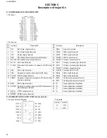
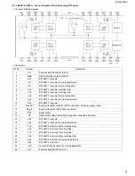
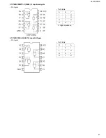
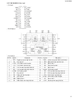
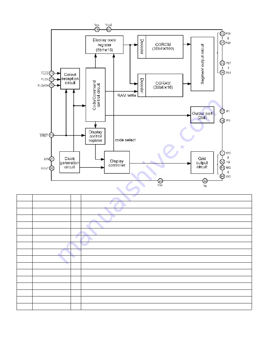
5.8 M66004SP(IC721):FL Driver
• Block diagram
• Pin function
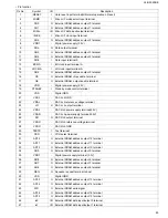
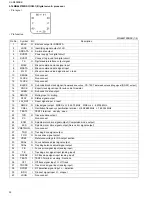
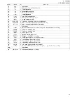
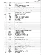
Pin.No.
Symbol
I/O
Description
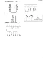
1~12
12G~1G
O
FL grid control signal output.
13
SRST
I
Reset signal input
14
FLCS
I
Chip select signal input.
15
FLCLK
I
Shift clock signal input.
16
FLDATA
I
Serial data input.
17
P1
O
Output port (static operation)
18
P0
O
Output port (static operation)
19
VCC1
-
Power supply for internal logic.
20
XOUT
O
Clock signal output.
21
XIN
I
Clock signal input.
22
VSS
-
Connect to ground.
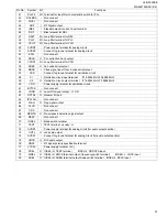
23~31
P36~P28
O
FL Segment control signal output.
32
VP
-
Power supply.
33~59
P27~P01
O
FL Segment control signal output.
60
VCC2
-
Power supply for grid output and segment output.
61~64
16G~13G
O
FL grid control signal output.
Содержание XL-R5020BK
Страница 5: ...XL R5020BK 5 1 7 Importance admistering point on the safety ...
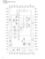
Страница 28: ...XL R5020BK 28 5 14TC94A02F 005 IC401 MP3 Decoder Block diagram ...
Страница 39: ...XL R5020BK 39 ...
Страница 123: ...0502KTYMDWJEM EN J VC VICTOR COMPANY OF JAPAN LIMITED ...


