


XL-R5020BK
36
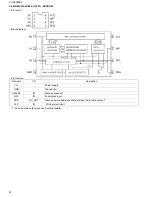
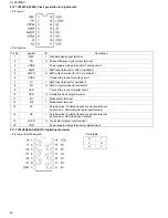
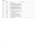
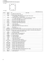
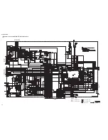
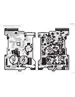
5.18UPD784215AGF513(IC501):System controller
• Pin layout
• Pin function
UPD784215AGF513 1/2
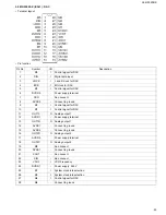
Pin No.
Symbol
I/O
Description
1
CKSL2
-
Not use
2
CKSL1
-
Not use
3
IDFS2
-
Not use
4
TEST-
I
Test mode input terminal L : Test mode
5
VR_STB
O Strobe signal output to IC891
6
VR_DATA
O Data output to IC891
7
VR_CK
O Clock signal output to IC891
8
NC
-
Non connect
9
VDD
-
Power supply te5V
10,11
CS1/CS2
I
Chip select terminal
12,13
JOGA/JOGB
I
Multi jog dial A/B input
14
FLDAT
O Serial data output to FL driver
15
FLCLK
O Shift clock signal output to FL driver
16
FLCS
O Chip select signal output to FL driver L : data output
17,18
NC
-
Non connect
19
PLL LOOK
I
PLL LOCK detect signal from IC404
20
DIN_COA
-
When digital input is coaxial for output H
21
NC
-
Non connect
22
VPP
-
Connect to ground
23
DIG_LED
O Digital LED control signal output L : Lighting
24
CD_LED
O 3CD LED control signal output L : Lighting
25
LIN_LED
O Line IN LED control signal output L : Lighting
26
MIC_LED
O MIC LED control signal output L : Lighting
27
CC LED
-
Non use
28
MIXBL
I
Mix balance volume level input
29
DIN_OPT
O When digital input is optical for output H
30
SMUTE
O System muting signal output
31
DACMUTE
O DAC muting signal output
32
CD_DRT
O It is a power output to the direct connection of analog recording
source 3CD to the A/D input of CD-RW as for L
33
SCD
O Analog recording source 3CD select control output
L : selected 3CD
34,35
SLIN1/SLIN2
O Analog recording source select control output
36
SMIC
O Analog recording source MIC select control output
L : selected MIC
37
VDD
-
Power supply te5V
(connects with the backup capacitor at power supply off. )
38
X2
O Main system clock output terminal 10MHz
39
X1
I
Main system clock input terminal 10MHz
40
VSS
-
Connect to ground
41
XT2
O Sub clock output terminal 32.768KHz
42
XT1
I
Sub clock input terminal 32.768KHz
43
RESET
I
Reset signal input
Содержание XL-R5020BK
Страница 5: ...XL R5020BK 5 1 7 Importance admistering point on the safety ...
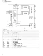
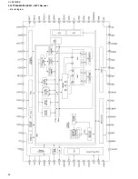
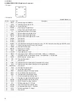
Страница 28: ...XL R5020BK 28 5 14TC94A02F 005 IC401 MP3 Decoder Block diagram ...
Страница 39: ...XL R5020BK 39 ...
Страница 123: ...0502KTYMDWJEM EN J VC VICTOR COMPANY OF JAPAN LIMITED ...


