


Functional Architecture
Intel® Server Board SE7520AF2 TPS
38
Revision
1.2
Intel order number C77866-003
can be routed to the front of the server. All five ports are high-speed, full-speed, and low-speed
capable.
3.1.4.8
Real-time Clock (RTC)
The ICH5-R contains a Motorola* MC146818A-compatible real-time clock with 256 bytes of
battery backed RAM. The real-time clock performs two key functions: keeping track of the time
of day and storing system data, even when the system is powered down. The RTC operates on
a 32.768 KHz crystal and a separate 3 V lithium battery. The RTC also supports two lockable
memory ranges. By setting bits in the configuration space, two 8-byte ranges can be locked to
read and write accesses. This prevents unauthorized reading of passwords or other system
security information.
3.1.4.9
General-purpose Input/Output (GPIO)
General-purpose inputs and outputs are provided for custom system design. The number of
inputs and outputs depends on the ICH5-R configuration. All unused GPI pins must be pulled
high or low, so that they are at a predefined level and do not cause undue side effects and must
meet the following guidelines:
GPIO 0:15 sticky bits on input, level triggered, 61µs min time for latch
GPI's only: 0:15, 40-47 (note: 42-47 unimplemented)
GPO's only: 16-23, 48-55 (note: 49-55 unimplemented)
GPI or GPO: 24-39 (note: 35-39 unimplemented, GPIO[33] is changed to SATA LED
and this GPIO is NOT available)
GPIO resume (3.3VSTBY) power well: 8-15, 24-25, 27-28
GPIO core (3.3V) power well: 0-7, 16-23, 32-34, 40-41, 48
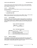
Table 3. ICH5-R GPIO Assignment
ICH5-R Signal
Type
Pin
PWR Well
Tolerance
Description
INTRUDER DETECT
Input
Y12
Core
3.3V
TP
GPI0/REQA
Input
A5
Core
5V
Board SKU 0
GPI1/REQB/REQ5#
Input
E7
Core
5V
Board SKU 1
GPI6/AGPBUSY#
Input
R5
Core
5V
Bios Recover Boot
GPI7 Input
U3
Core
5V
MCH
PME
GPI8 Input
Y2
Resume
3.3V
WAKE#/PCI
PME#
GPI9/OC[4]# Input
B14
Resume
3.3V
Reserved for USB OC4
(3 in back, 2 in front)
GPI10/OC[5]# Input
A14
Resume
3.3V
MCH
GPE
GPI11/SMBALERT# Input
AC3
Resume
3.3V
Board ID 0
GPI12 Input
W4
Resume
3.3V
SIO
SMI
GPI13
Input
W5
Resume
3.3V
BMC IRQ SMI
GPI14/OC[6]#
Input
D13
Resume
3.3V
SIO > ICH5R PME
GPI15/OC[7]# Input
C13
Resume
3.3V
Password
clear
GPO16/GNTA# Output
E8
Core
3.3V
TP
GPO17/GNTB#/GNT[5]# Output B4 Core
3.3V
TP


