background image

Platform Management 

Intel® Server Board SE7520AF2 TPS 

150  

Revision 

1.2 


Intel order number C77866-003 

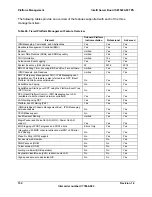
The following tables provide an overview of the features supported with each of the three 
management tiers: 

Table 66. Tiered Platform Management Feature Overview 

Element 

Onboard Platform 

Instrumentation Professional Advanced 

IPMI Messaging, Commands, and Abstractions 

Yes 

Yes 

Yes 

Baseboard Management Controller (BMC) 

Yes 

Yes 

Yes 

Sensors Limited 

Yes 

Yes 

Sensor Data Records (SDRs) and SDR Repository 

Limited 

Yes 

Yes 

FRU Information 

Limited 

Yes 

Yes 

Autonomous Event Logging 

Yes 

Yes 

Yes 

System Event Log (SEL) Entries 

92  

3276  

3276  

BMC Watchdog Timer, covering BIOS and Run-Time software 

Limited 

Yes 

Yes 

IPMI Channels, and Sessions 

Limited 

Yes 

Yes 

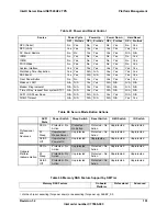
EMP (Emergency Management Port) - IPMI Messaging over 
Serial/Modem. This feature is also referred to as DPC (Direct 
Platform Control) over serial/modem. 

No 

Yes 

Yes 

Serial/Modem Paging 

No 

Yes 

Yes 

Serial/Modem Alerting over PPP using the Platform Event Trap 
(PET) format 

No 

Yes 

Yes 

DPC (Direct Platform Control) - IPMI Messaging over LAN 
(available via both on-board network controllers) 

Yes 

Yes 

Yes 

LAN Alerting using PET 

Yes 

Yes 

Yes 

Platform Event Filtering (PEF) 

Yes 

Yes 

Yes 

ICMB (Intelligent Chassis Management Bus) - IPMI Messaging 
between chassis 

No 

Yes 

Yes 

PCI SMBus support 

No 

Yes 

Yes 

Fault Resilient Booting 

Limited 

Yes 

Yes 

Magic Packet and Wake On LAN (WOL) / Power On LAN 
support Yes 

Yes 

Yes 

BIOS logging of POST progress and POST errors 

Errors Only 

Yes 

Yes 

Integration with BIOS console redirection via IPMI v2.0 Serial 
Port Sharing 

No 

Yes 

Yes 

Wake On Ring (WOR) support 

No 

Yes 

Yes 

Access via web browser 

No 

No 

Yes 

SNMP access (OOB) 

No 

No 

Yes 

Telnet access (OOB) 

No 

No 

Yes 

Alerting via Email (OOB operation) 

No 

No 

Yes 

Keyboard/Video/Mouse (KVM) redirection via LAN 

No 

No 

Yes 

High-speed access to dedicated NIC 

No 

No 

Yes 

Содержание SE7520AF2

Страница 1: ...Intel Server Board SE7520AF2 Technical Product Specification Intel order number C77866 003 Revision 1 2 March 2005 Enterprise Platforms and Services Marketing ...

Страница 2: ...ions 01 2004 0 5 First release 05 2004 0 97 Second release 05 2004 0 99 Added integrated Intel RAID Controller SROMBU42E Chapter 08 2004 1 0 First public release 01 2005 1 1 Q1 2005 Update rolled Spec Update documentation changes and updated BIOS Setup screen changes 03 2005 1 2 Updated mBMC and Intel Management Module platform sensors tables ...

Страница 3: ...erty right Intel products are not intended for use in medical life saving or life sustaining applications Intel may make changes to specifications and product descriptions at any time without notice Designers must not rely on the absence or characteristics of any features or instructions marked reserved or undefined Intel reserves these for future definition and shall have no responsibility whatso...

Страница 4: ...Table of Contents Intel Server Board SE7520AF2 TPS Revision 1 2 Intel order number C77866 003 iv This page intentionally left blank ...

Страница 5: ...29 3 1 Intel E7520 Chipset 30 3 1 1 Memory Controller Hub MCH 30 3 1 2 PCI X Hub PXH 34 3 1 3 IOP332 I O Processor 35 3 1 4 I O Controller Hub ICH5 R 35 3 2 Processor Sub system 39 3 2 1 Processor VRD 40 3 2 2 Reset Configuration Logic 40 3 2 3 Processor Module Presence Detection 40 3 2 4 GTL2006 41 3 2 5 Common Enabling Kit CEK Design Support 41 3 3 Memory Sub System 41 3 3 1 Supported Memory 42 ...

Страница 6: ...ution 81 4 Integrated Intel RAID Controller SROMBU42E 83 4 1 Overview 83 4 2 Primary Integrated Intel RAID Controller SROMBU42E Features 83 4 2 1 Configuration on Disk 85 4 2 2 Array Performance Features 85 4 2 3 Fault Tolerance Capabilities 85 4 3 RAID Software Stack 86 4 3 1 General RAID Features 86 4 3 2 RAID Level Migration 87 4 3 3 Fault Tolerant Features 87 4 3 4 Cache Options and Settings 8...

Страница 7: ...S 105 5 1 BIOS Identification String 105 5 2 Supported BIOS Features 105 5 3 Processor Initialization 106 5 3 1 Multiple Processor Initialization 106 5 3 2 Mixed Processor Steppings 107 5 3 3 Mixed Processor Models 107 5 3 4 Mixed Processor Families 107 5 3 5 Mixed Processor Cache Sizes 107 5 3 6 Jumperless Processor Speed Settings 107 5 3 7 Microcode 108 5 3 8 Processor Cache 108 5 3 9 Hyper Thre...

Страница 8: ...alization 116 5 5 13 Removable Media Initialization 117 5 6 Flash ROM 117 5 7 BIOS User Interface 117 5 7 1 System State Window 118 5 7 2 Logo Diagnostic Window 118 5 7 3 Current Activity Window 118 5 8 System Diagnostic Screen 118 5 8 1 Static Information Display 118 5 9 Quiet Boot OEM Splash Screen 119 5 10 BIOS Boot Popup Menu 119 5 11 BIOS Setup Utility 119 5 11 1 Localization 120 5 11 2 Conso...

Страница 9: ...t Architecture Overview 149 6 1 1 Tiered Server Management Model 149 6 1 2 5V Standby 153 6 1 3 IPMI Messaging Commands and Abstractions 154 6 1 4 IPMI Sensor Model 154 6 1 5 Private Management Bus 155 6 1 6 Management Controllers 156 6 2 Onboard Platform Instrumentation Management Features and Functionality 158 6 2 1 mBMC Self test 159 6 2 2 SMBus Interfaces 159 6 2 3 External Interface to mBMC 1...

Страница 10: ...t of Failed Processors 191 7 2 Error Logging 192 7 2 1 Error Sources and Types 192 7 2 2 SMI Handler 192 7 2 3 BIOS Generated IPMI Events 197 7 2 4 Single Bit ECC Error Throttling Prevention 198 7 3 Error Messages and Error Codes 199 7 3 1 POST Progress Codes and Messages 199 7 3 2 BIOS Messages 206 7 3 3 POST Error Messages and Handling 212 7 3 4 Boot Block Error Beep Codes 215 7 3 5 POST Error B...

Страница 11: ...n Jumper 242 10 General Specifications 243 10 1 Absolute Maximum Ratings 243 10 2 Processor Power Support 243 10 3 SE7520AF2 Power Budget 244 10 4 Power Supply Specifications 244 10 4 1 Power Timing 244 10 4 2 Voltage Recovery Timing Specifications 246 11 Product Regulatory Compliance 249 11 1 1 Product Safety Compliance 249 11 1 2 Product EMC Compliance 249 11 1 3 Product Regulatory Compliance Ma...

Страница 12: ...tel Server Board SE7520AF2 TPS Revision 1 2 Intel order number C77866 003 xii 11 2 7 BSMI Taiwan 251 11 3 Replacing the Back Up Battery 251 Integration and Usage Tips I Glossary II Reference Specifications and Documents V ...

Страница 13: ...12 Intel Portable Cache Module 63 Figure 13 Video Controller PCI Bus Interface 67 Figure 14 Intel Xeon Processor Memory Address Space 71 Figure 15 DOS Compatibility Region 72 Figure 16 Extended Memory Map 74 Figure 17 CONFIG_ADDRES Register 79 Figure 18 Intel RAID Activation Key 83 Figure 19 RAID 0 90 Figure 20 RAID 1 90 Figure 21 RAID 5 91 Figure 22 RAID 5 91 Figure 23 RAID 50 92 Figure 24 Inte R...

Страница 14: ...Managment Architecture 153 Figure 36 mBMC in a Server Management System 159 Figure 37 External Interfaces to mBMC 160 Figure 38 IPMI over LAN 163 Figure 39 Power Supply Control Signals 170 Figure 40 Location of Diagnostic LEDs on Baseboard 200 Figure 41 SE7520AF2 Configuration Jumpers J1D1 241 Figure 42 SE7520AF2 BIOS Bank Jumper J2J6 242 Figure 43 Output Voltage Timing 245 Figure 44 Turn on off T...

Страница 15: ...Connections 54 Table 14 IOP332 P64 A Configuration IDs 54 Table 15 IOP332 P64 B Configuration IDs 55 Table 16 IOP332 P64 B Arbitration Connections 55 Table 17 IOP332 P64 B Arbitration Connections 55 Table 18 PCI Interrupt Routing Sharing 56 Table 19 Interrupt Definitions 57 Table 20 Intel Server Board SE7520AF2 Video Modes 65 Table 21 Video Memory Interface 66 Table 22 NIC2 Status LED 68 Table 23 ...

Страница 16: ...uration Sub menu Selections 128 Table 49 BIOS Setup PCI Configuration Sub menu Selections 128 Table 50 BIOS Setup Memory Configuration Sub menu Selections 129 Table 51 BIOS Setup Boot Menu Selections 131 Table 52 BIOS Setup Boot Settings Configuration Sub menu Selections 131 Table 53 BIOS Setup Boot Device Priority Sub menu Selections 132 Table 54 BIOS Setup Hard Disk Drive Sub Menu Selections 132...

Страница 17: ...ors for the Intel Management Module 180 Table 82 Memory Error Events 194 Table 83 Examples of Event Data Field Contents for Memory Errors 195 Table 84 PCI error events 195 Table 85 Event Data Field Contents for PCI Errors 196 Table 86 FRB 2 Error Events 196 Table 87 Event Data Field Contents for FRB 2 Errors 197 Table 88 BIOS Generated IPMI Events 197 Table 89 POST Progress Code LED Example 199 Ta...

Страница 18: ...der Pin out J1A1 228 Table 118 IPMB Header Pin out J1G1 229 Table 119 IPMB Header Pin out J1B2 229 Table 120 HSBP Header Pin out J1K3 J1K2 229 Table 121 PCI Slot Characteristics 230 Table 122 Slot 1 and 5 PCI X 64bit 3 3V Pin out J1D4 J4D1 230 Table 123 Slot 3 and 4 PCI Express Pin out J2C1 J3C1 231 Table 124 Slot 6 PCI X 64 bit 3 3V Pin out J4D2 Riser Capable 232 Table 125 Front Panel 34 Pin Head...

Страница 19: ... 6 pin System Fan Headers Pin out J2K4 J2K2 240 Table 140 Configuration Jumper Options 241 Table 141 BIOS Bank Jumper Option 242 Table 142 Absolute Maximum Ratings 243 Table 143 Intel Xeon processor DP TDP Guidelines 243 Table 144 SE7520AF2 Power Budget 244 Table 145 SE7520AF2 Power Supply Voltage Specification 244 Table 146 Voltage Timing Parameters 245 Table 147 Turn On Off Timing 245 Table 148 ...

Страница 20: ...List of Tables Intel Server Board SE7520AF2 TPS Revision 1 2 Intel order number C77866 003 xx This page intentionally left blank ...

Страница 21: ... systems can be obtained by ordering the External Product Specification EPS or External Architecture Specification EAS for a given sub system The EPS documents available for this server board include the following Intel Server Board SE7520AF2 BIOS EPS Mini Baseboard Management Controller mBMC EPS Intel Server Board SE7520AF2 Baseboard Management Controller BMC EPS Server Management EAS Hot Swap Co...

Страница 22: ...e used together the fully integrated platform will meet the intended thermal requirements of these components It is the responsibility of the platform integrator who chooses not to use Intel developed server building blocks to consult vendor datasheets and operating parameters to determine the amount of airflow required for their specific application and environmental conditions Intel Corporation ...

Страница 23: ... Socket 604 and 800 MT s Front Side Bus Intel E7520 Memory Controller Hub MCH Intel 6700PXH PCI X Controller Hub PXH Intel 80332 I O Processor with Intel XScale Technology IOP332 Intel 82801ER I O Controller Hub5 ICH5 R Support for eight DDR2 400MHz compliant registered ECC DIMMs providing up to 16GB of memory in a dual channel architecture Five full length full height PCI expansion slots PCI Slot...

Страница 24: ...viding two optional USB ports for front panel support Two stacked PS 2 ports for keyboard and mouse interchangeable Two serial ports One external serial port Serial A on the rear I O area of the board and one internal header is also available providing an optional port Serial B One IDE connector supporting up to two ATA 100 compatible devices One standard floppy drive interface Six multi speed sys...

Страница 25: ...0 PCI X Hub PXH Intel IO Controller Hub ICH5 R LSI 53C1030 Dual U320 Controller SCSI SIO mBMC Intel 80332 I O Processor IOP332 ATA 100 Primary Floppy Intel RAID Key Intel 82546GB Gb Ethernet NIC ATI RAGE XL VGA SCSI CH_A SCSI CH_B DIMM 1B DIMM 1A DIMM 2B DIMM 2A DIMM 3B DIMM 3A DIMM 4B DIMM 4A CPU_1 FAULT LED CPU_2 FAULT LED CPU_1 FAN CPU_2 FAN SLOT1 PCI X 64 133 HP SLOT2 RAID DIMM SLOT3 PCI EXP x...

Страница 26: ...rview Intel Server Board SE7520AF2 TPS 26 Revision 1 2 Intel order number C77866 003 2 3 2 Mechanical Drawing The following mechanical drawing shows the physical dimensions of the server board Figure 2 Board Dimensions ...

Страница 27: ...rd SE7520AF2 TPS Server Board Overview Revision 1 2 27 Intel order number C77866 003 2 3 3 ATX I O Layout The following figure shows the ATX rear I O layout of the Server Board SE7520AF2 Figure 3 ATX Rear IO Connectors ...

Страница 28: ...Server Board Overview Intel Server Board SE7520AF2 TPS 28 Revision 1 2 Intel order number C77866 003 This page intentionally left blank ...

Страница 29: ...vision 1 2 29 Intel order number C77866 003 3 Functional Architecture This chapter provides a high level description of the functionality associated with the architectural blocks that comprise the Intel Server Board SE7520AF2 Figure 4 Server Board Block Diagram ...

Страница 30: ... with the LSI Logic 53C1030 SCSI controller to provide RAID functionality 3 1 1 Memory Controller Hub MCH The MCH is a 1077 ball FC BGA package which supports the following interfaces CPU Front Side Bus at 200MHz operation using AGTL Assisted Gunner Transceiver Logic signaling 4x 64 bit data bus at 6 4GB s Dual memory channels supporting registered 64 bit data ECC DDR2 400MHz DIMMs with bandwidth ...

Страница 31: ...s for one DIMM per channel to be held in reserve and brought on line if another DIMM in the channel becomes defective DIMM sparing and memory mirroring are mutually exclusive of one another Hardware periodic memory scrubbing including demand scrub support Retry on uncorrectable memory errors Intel x4 Single Device Data Correction SDDC for memory error detection and correction of any number of bit ...

Страница 32: ... performs a retry of that packet and all following packets Although this causes a temporary interruption in the delivery of packets the retry helps to maintain the link integrity 3 1 1 3 3 PCI Express Link Recovery If excessive errors occur the hardware may determine that the quality of the connection is in question and the end points can enter a quick training sequence known as recovery The width...

Страница 33: ...may NOT be added or removed Slot power in transition on off or off on PCI adapter may NOT be added or removed Attention LED Normal operation Slot on attention power fault or operational problem present on the slot Slot being identified at the user s request to locate the slot via the Hot Plug Interface Driver 3 1 1 3 7 PCI Express Hot Plug Controller The PCI Express hot plug solution is supported ...

Страница 34: ... speed of 100MHz with all loads present on the segment Slot also enables optional support for third party one or two slot riser Intel 10 100 1000 82546GB Dual Gigabit Ethernet controller 3 1 2 1 PCI X Hot Plug Option Hot plug support is available on the PCI X expansion Slot 5 and Slot 1 from the IOP332 I O processor discussed in a later section on the SE7520HPAF2 SKU The PCI X hot plug controller ...

Страница 35: ...secondary PCI device The upstream PCI Express port implements the PCI to PCI bridge programming model according to the PCI Express Specification Rev 1 0 The primary ATU is compliant with the Addendum to the PCI Local Bus Specification Rev 1 0a definitions of an application bridge The IOP332 I O processor is fully compliant with the PCI Local Bus Specification Rev 2 3 and the PCI Express Specificat...

Страница 36: ...ntel Server Board SE7520AF2 This integrated functionality provides the interface for IDE hard disks and ATAPI devices Each IDE device can have independent timings The IDE interface supports PIO IDE transfers up to 16 MB sec and Ultra ATA transfers up 100 MB sec The IDE interface integrates 16x32 bit buffers for optimal transfers and does not consume any ISA DMA resources The ICH5 R s IDE signal ch...

Страница 37: ...C interface Channels 0 3 are 8 bit channels Channels 5 7 are 16 bit channels Channel 4 is reserved as a generic bus master request The timer counter block contains three counters that are equivalent in function to those found in one 82C54 programmable interval timer These three counters are combined to provide the system timer function and speaker tone The 14 31818 MHz oscillator input provides th...

Страница 38: ...r low so that they are at a predefined level and do not cause undue side effects and must meet the following guidelines GPIO 0 15 sticky bits on input level triggered 61µs min time for latch GPI s only 0 15 40 47 note 42 47 unimplemented GPO s only 16 23 48 55 note 49 55 unimplemented GPI or GPO 24 39 note 35 39 unimplemented GPIO 33 is changed to SATA LED and this GPIO is NOT available GPIO resum...

Страница 39: ...l I2 C commands are implemented The SMBus host controller for the ICH5 R provides a mechanism for the processor to initiate communications with SMBus peripherals slaves The ICH5 R supports slave functionality including the Host Notify protocol Hence the host controller supports eight command protocols of the SMBus interface Quick Command Send Byte Receive Byte Write Byte Word Read Byte Word Proces...

Страница 40: ...rts the Flexible Mother Board FMB specification for all Nocona Irwindale processors with respect to current requirements and processor speed requirements FMB is an estimation of the maximum values the Nocona Irwindale versions of the Intel Xeon processors will have over their lifetime The value is an estimate specifications for future processors may differ At present the current demand per FMB is ...

Страница 41: ...CEK processor mounting and thermal solution The baseboard ships from Intel s factory with a CEK spring snapped onto the underside of the board beneath each processor socket The CEK spring is removable to allow the use of non Intel heat sink retention solutions Note When installing the server board into an Intel Server Chassis SC5300 the passive heatsink solution no fan must be used Figure 5 CEK Pa...

Страница 42: ...registered DDR2 400 DIMMs per channel which provides a total of eight DIMMs The maximum memory capacity supported is 16 GB using eight modules of 1 Gbit DRAM technology devices Table 5 SE7520AF2 Supported DIMM Modules Technology Organization DRAM Components DIMM Row Column Address Bits 4M X 8 X 4bks 8 12 10 128Mb 8M X 4 X 4bks 16 12 11 8M X 8 X 4bks 8 13 10 256Mb 16M X 4 X 4bks 16 13 11 16M X 8 X ...

Страница 43: ... up to 16 GB of system memory capacity Support a maximum of four ranks per channel1 Serial PD JEDEC Rev 2 0 Voltage options 1 8 V VDD VDDQ Interface SSTL2 Two DIMMs must be populated in a bank for a x144 wide memory data path DIMMs must be populated beginning with the socket furthest away from the MCH i e DIMM 1B and DIMM 1A DIMMs must be identical within the same bank For example the DIMM in sock...

Страница 44: ...eve DIMM information needed to program the MCH memory registers The following table provides the I2 C addresses for each DIMM slot Table 6 I2 C Addresses for Memory Module SMB Device Address DIMM 1A 0xA6 DIMM 1B 0xAE DIMM 2A 0xA4 DIMM 2B 0xAC DIMM 3A 0xA2 DIMM 3B 0xAA DIMM 4A 0xA0 DIMM 4B 0xA8 3 3 5 Memory Voltage Margining The supply voltage for memory devices is 1 8V The Intel Server Board SE752...

Страница 45: ...ring fail down as it does have significant performance impacts in that environment 3 3 6 2 Integrated Memory Scrub Engine The Intel E7520 MCH includes an integrated engine to walk the populated memory space proactively seeking out soft errors in the memory subsystem In the case of a single bit correctable error this hardware detects logs and corrects the data except when an incoming write to the s...

Страница 46: ...s with good ECC This speeds up the mandatory memory initialization step and frees the processor to pursue other machine initialization and configuration tasks Additional features have been added to the initialization engine to support high speed population and verification of a programmable memory range with one of four known data patterns 0 F A 5 3 C and 6 9 This function facilitates a limited ve...

Страница 47: ... victim DIMM if multiple DIMMs have crossed the threshold prior to sparing invocation and software must initiate the memory copy Hardware automatically isolates the failed DIMM after the copy has completed The data copy is accomplished by address aliasing within the DDR control interface thus it does not require reprogramming of the DRAM row boundary DRB registers nor does it require notification ...

Страница 48: ... M 4 A Primary Empty Empty Mirror Figure 7 Four DIMM Memory Mirror Configuration A six DIMM population uses identical devices within DIMM Bank 1 and between DIMM Banks 2 and 3 Referring to Figure 8 DIMMs labeled 3A 3B 2A and 2B must be single rank and identical and those labeled 1A and 1B must be dual ranked and identical The first group does not have to be identical to those in the second group ...

Страница 49: ... B D I M M 4 A Empty Mirror Primary Primary Mirror Figure 8 Six DIMM Memory Mirror Configuration An eight DIMM population uses identical devices in DIMM Banks 1 and 2 and in DIMM Banks 3 and 4 Referring to Figure 9 DIMMs labeled 1A 1B 2A and 2B must be identical and those labeled 3A 3B 4A and 4B must be identical The first group does not need to be identical to those in the second group ...

Страница 50: ...le on each channel Hardware in the MCH tracks which DIMM slots are primaries and which are mirrors such that data may be internally realigned to correctly reassemble cache lines regardless of which copy is retrieved There are four distinct cases for retrieval of the even and odd chunks of a cache line of data Interleaved dual channel read to the primary DIMM with even data on channel A Interleaved...

Страница 51: ...ne may be activated during initialization The feature can be enabled in system BIOS setup The selected feature must remain enabled until the next power cycle 3 4 I O Sub System The I O sub system is comprised of several components The MCH provides the PCI Express interface to PCI Express slots 3 and 4 The PXH provides the PCI X interface for the dual gigabit Ethernet controller and PCI X slots 5 a...

Страница 52: ... 31 16 which acts as a chip select on the PCI bus segment in configuration cycles This determines a unique PCI device ID value for use in configuration cycles The following table shows the bit to which each IDSEL signal is attached for the 32 bit on board device Table 8 ICH5 R P32 A Configuration IDs IDSEL Value Device 28 ATI Rage XL video controller 3 4 1 1 2 ICH5 R P32 A Arbitration The ICH5 R P...

Страница 53: ...signal connected to one bit of AD 31 16 which acts as a chip select on the PCI bus segment in configuration cycles This determines a unique PCI device ID value for use in configuration cycles The following table shows the bit to which each IDSEL signal is attached for PXH P64 A P64 B devices and corresponding device description Table 10 PXH P64 A Configuration IDs IDSEL Value Device 17 Slot 5 PCI ...

Страница 54: ...rnet controller PXH_PBREQ1 PXH_PBGNT1 Slot 6 PCI X 64 100 PXH_PBREQ1 PXH_PBGNT1 Slot 6 Upper slot of optional 2 slot riser PXH_PBREQ2 PXH_PBGNT2 Slot 7 Lower slot of optional 2 slot riser 3 4 1 3 IOP332 P64 A and P64 B 64 bit 133 MHz PCI Subsystem The two peer 64 bit PCI X bus segments are directed through the IOP332 I O bridge The first PCI X segment P64 A supports the interface to the on board L...

Страница 55: ...idge PCI interface arbitration lines PBREQx and PBGNTx are a special case in that they are internal to the host bridge The following table defines the arbitration connections Table 17 IOP332 P64 B Arbitration Connections Baseboard Signals Device IOP_PBREQ0 IOP_PBGNT0 Slot 1 PCI X 64 133 3 4 1 4 MCH PExp B and PExp C x8 x4 PCI Express PCI Subsystem The PCI Express PExp B and PExp C segments are ena...

Страница 56: ...ATA ICH5R_PIRQC Video ICH5R_PIRQB SIO ICH5R_SERIRQ Legacy IDE ICH5R_IRQ14 82546GB 1 PXH_PBIRQ4 82546GB 2 PXH_PBIRQ5 SCSI Controller 1 IOP_XINT0 SCSI Controller 2 IOP_XINT1 Slot 1 PCI X 64 133 IOP_XINT4 IOP_XINT5 IOP_XINT6 IOP_XINT7 Slot 3 PCI EXP x4 NA NA NA NA Slot 4 PCI EXP x8 NA NA NA NA Slot 5 PCI X 64 133 PXH_PAIRQ0 PXH_PAIRQ1 PXH_PAIRQ2 PXH_PAIRQ3 Slot 6 PCI X 64 100 PXH_PBIRQ0 PXH_PBIRQ1 PX...

Страница 57: ...ary ATA legacy mode PIRQA USB 1 1 controller 1 and 4 PIRQB Video PIRQC USB 1 1 controller 3 Native IDE SATA PIRQD USB 1 1 controller 2 PIRQE Option for SCI TCO HPET 0 1 2 PIRQF Option for SCI TCO HPET 0 1 2 PIRQG Option for SCI TCO HPET 0 1 2 PIRQH USB 2 0 EHCI controller 1 Option for SCI TCO HPET 0 1 2 Ser IRQ SIO3 3 4 2 4 Serialized IRQ Support The Intel Server Board SE7520AF2 supports a seriali...

Страница 58: ... IRQ9 IRQ10 IRQ11 IRQ12 IRQ13 IRQ14 IRQ15 IRQ16 IRQ17 IRQ18 ICH5 R IOAPIC 0 MCH HI 1 5 ICH5 R 8259PIC IRQ0 IRQ1 IRQ2 IRQ3 IRQ4 IRQ5 IRQ6 IRQ7 IRQ8 IRQ9 IRQ10 IRQ11 IRQ12 IRQ13 IRQ14 IRQ15 IRQ16 IRQ17 IRQ18 PXH IOAPIC 1 IRQ0 IRQ1 IRQ2 IRQ3 IRQ4 IRQ5 IRQ6 IRQ7 IRQ8 IRQ9 IRQ10 IRQ11 IRQ12 IRQ13 IRQ14 IRQ15 IRQ16 IRQ17 IRQ18 PXH IOAPIC 2 CPU1 CPU2 INTR INTR HL 1 5 PCI E INTERFACE PCI E INTERFACE ICH5 ...

Страница 59: ... Port1 ISA ISA Floppy ISA ISA RTC SCI ISA ISA ISA Mouse ISA Coprocessor Error P IDE ISA Not Used Cascade Serialized IRQ Interface SERIRQ ICH5 R Interrupt Routing SERIRQ USB 1 1 1 and 4 Video USB 1 1 3 Native IDE and S ATA PIRQD PIRQE PIRQF PIRQG PIRQH USB 1 1 2 Option for SCI TCO HPET 0 1 2 Option for SCI TCO HPET 0 1 2 Option for SCI TCO HPET 0 1 2 USB 2 0 EHCI Controller 1 Option for SCI TCO HPE...

Страница 60: ...erformance SCSI Ultra320 cores and a 64 bit 133 MHz PCI X bus master DMA core The LSI Logic 53C1030 employs three ARM966E S processors to meet the data transfer flexibility requirements of the Ultra320 SCSI PCI and PCI X specifications Separate ARM processors support each SCSI channel and the PCI PCI X interface These processors implement the LSI Logic Fusion MPT architecture a multithreaded I O a...

Страница 61: ...ized architecture Three ARM966E S processors provide high performance with low latency Two independent Ultra320 SCSI channels Designed for optimal packetized performance Uses proven integrated LVDlink transceivers for direct attach to either LVD or SE SCSI buses with precision controlled slew rates Supports expanded communication protocol ECP Supports Integrated Mirroring IM which provides feature...

Страница 62: ...ding split transactions Supports Message Signaled Interrupts MSI 3 4 4 RAID Functionality The Intel Server Board SE7520AF2 enables RAID on MotherBoard ROMB through the integrated Intel RAID Controller SROMBU42E This solution is comprised of the Intel 80332 I O Processor with XScale Technology in conjunction with the onboard LSI Logic 53C1030 SCSI controller and resident RAID firmware on the server...

Страница 63: ... or 512 MB DDR333 un buffered ECC DIMM enabling higher performance operation write back cache For enhanced data protection and maximum performance the ROMB functionality on the Intel Server Board SE7520AF2 supports the Intel Portable Cache Module accessory which provides up to 72 hours of battery back up The Intel Portable Cache Module accessory is shown below Figure 13 Intel Portable Cache Module...

Страница 64: ...regardless of the UDMA mode reported by the SATA device or the system BIOS The SATA interface from the ICH5 R supports data transfer rates up to 1 5 Gb s 150 MB s 3 4 6 1 Intel Embedded Server RAID Technology The Intel Server Board SE7520AF2 enables SATA RAID known as the Intel Embedded Server RAID Technology This solution is available via the 82801ER ICH5 R ICH5R and offers data stripping for hig...

Страница 65: ...D 3D modes supported for both CRT and LCD Table 20 Intel Server Board SE7520AF2 Video Modes 2D Video Mode Support 2D Mode Refresh Rate Hz 8 bpp 16 bpp 24 bpp 32 bpp 640x480 60 72 75 90 100 Supported Supported Supported Supported 800x600 60 70 75 90 100 Supported Supported Supported Supported 1024x768 60 72 75 90 100 Supported Supported Supported Supported 1280x1024 43 60 Supported Supported Suppor...

Страница 66: ...ng performance The Intel Server Board SE7520AF2 supports an 8MB 512Kx32bitx4 banks SDRAM device for video memory The following table shows the video memory interface signals Table 21 Video Memory Interface Signal Name I O Type Description CAS O Column Address Select CKE O Clock Enable for memory CS 1 0 O Chip Select for memory DQM 7 0 O Memory Data Byte Mask DSF O Memory Special Function Enable HC...

Страница 67: ...ert on LAN functionality Both channels can be disabled through the BIOS Setup Utility The 82546EB supports the following features 64 bit PCI X Rev 1 0 master interface Integrated IEEE 802 3 10Base T 100Base TX and 1000Base TX compatible PHY IEEE 820 3ab auto negotiation support Full duplex support at 10 Mbps 100Mbps and 1000 Mbps operation Integrated UNDI ROM support MDI MDI X and HWI support Low ...

Страница 68: ... I O device This chip contains the necessary circuitry to control two serial ports a floppy disk drive and PS 2 compatible keyboard and mouse The Intel Server Board SE7520AF2 supports the following features General Purpose Input Output GPIO Two serial ports Floppy controller Keyboard and mouse controller Wake up control 3 4 10 1 General Purpose Input Output GPIO The National Semiconductor PC87427 ...

Страница 69: ...tor located on the back I O area of the baseboard enabling Serial Port A One 9 pin DH 10 header on the server board enables an optional Serial Port B Serial Port B is an optional port accessed through a on board 9 pin internal DH 10 header A standard DH 10 to DB9 cable can be used to direct Serial Port A out the back or front of a chassis Table 24 Serial A Header Pin out Pin Signal Name Serial Por...

Страница 70: ...memory component that provides 2048Kb x 16 of BIOS and non volatile storage space The flash device is connected through the X bus from the SIO 3 5 Configuration and Initialization This section describes the initial programming environment including address maps for memory and I O techniques and considerations for programming ASIC registers and hardware option configuration 3 5 1 Memory Space At th...

Страница 71: ...f memory below 1 MB was defined for early PCs and must be maintained for compatibility The region is divided into subregions as shown in the following figure 4GB Optional ISA Hole Top of Low Memory TOLM 16MB 15MB 1MB 640KB 512KB 0 Additional Main Memory Address Range Main Memory Address Range DOS Legacy Address Range Lo PCI Memory Space Range TSEG SMRAM 64GB Hi PCI Memory Address Range Upper Memor...

Страница 72: ... 1 2 ISA Window Memory The ISA window memory is 128 KB between the address of 080000h to 09FFFFh This area can be mapped to the PCI bus or main memory Mappable to PCI or ISA memory Main memory only PCI only Shadowed in main memory 000000h 07FFFFh 080000h 09FFFFh 0A0000h 0BFFFFh 0C0000h 0DFFFFh 0E0000h 0EFFFFh 0F0000h 0FFFFFh 1MB 960KB 896KB 768KB 640KB 512KB 0 System BIOS Extended System BIOS Add ...

Страница 73: ...5 Extended System BIOS This 64 KB region from 0E0000h to 0EFFFFh is divided into four blocks of 16 KB each and may be mapped with programmable attributes to map to either main memory or to the PCI bus Typically this area is used for RAM or ROM This region can also be used extended SMM space 3 5 1 1 6 System BIOS The 64 KB region from 0F0000h to 0FFFFFh is treated as a single block By default this ...

Страница 74: ...he PCI bus memory space The remainder of this space up to 8 GB is always mapped to main memory unless TBSG SMM is used just under TOLM The range can be from 128KB up to 1MB 1MB depends on the BIOS setting which limits the top of memory to 256MB The BIOS occupies 512KB for 32 bit SMI handler Main Memory Address Region FFFFFFFFh FFE00000h FEC0FFFFh FEC00000h Top of Low Memory TOLM Depends on install...

Страница 75: ...el r Nocona and Irwindale processor based system can have up to 64 GB of addressable memory However the Intel E7520 chipset supports only 16 GB of addressable memory The BIOS uses the extended addressing mechanism to use the address ranges 3 5 1 3 Memory Shadowing The system BIOS and option ROM can be shadowed in main memory This is done to allow ROM code to execute more rapidly out of RAM ROM is ...

Страница 76: ...1 0 Disable Enable Disable 1 1 1 Disable Enable Enable 3 5 2 I O Map The Intel Server Board SE7520AF2 allows I O addresses to be mapped to the processor bus or through designated bridges in a multi bridge system Other PCI devices including the ICH5 R have built in features that support PC compatible I O devices and functions which are mapped to specific addresses in I O space On the Intel Server B...

Страница 77: ...65h NMI Status and Control Register Aliased 0067h NMI Status and Control Register Aliased 0070h NMI Mask bit 7 and RTC address bits 6 0 0072h NMI Mask bit 7 and RTC address bits 6 0 Aliased from 0070h 0074h NMI Mask bit 7 and RTC address bits 6 0 Aliased from 0070h 0076h NMI Mask bit 7 and RTC address bits 6 0 Aliased from 0070h 0071h RTC Data 0073h RTC Data Aliased from 0071h 0075h RTC Data Alias...

Страница 78: ...Port 1 Primary 03C0h 03CFh Video Display Controller 03D4h 03Dah Color Graphics Controller 03E8h 03Efh Serial Port A 03F0h 03F5h Floppy Disk Controller 03F6h 03F7h Primary IDE Sec Floppy 03F8h 03FFh Serial Port A primary 0400h 043Fh DMA Controller 1 Extended Mode Registers 0461h Extended NMI Reset Control 0480h 048Fh DMA High Page Register 04C0h 04CFh DMA Controller 2 High Base Register 04D0h 04D1h...

Страница 79: ...gure Bits 23 16 choose a specific bus in the system Bits 15 11 choose a specific device on the selected bus Bits 10 8 choose a specific function in a multi function device Bit 8 2 select a specific register in the configuration space of the selected device or function on the bus Figure 18 CONFIG_ADDRES Register 3 5 3 1 1 Bus Number PCI configuration space protocol requires that all PCI buses in a ...

Страница 80: ...SB UHCI controller 2 00 29 01 ICH5R USB UHCI controller 3 00 29 02 ICH5R USB 2 0 EHCI controller 00 29 07 Slot 1 PCI X 64 133 AD21 01 01 Slot 3 PCI EXP x4 01 04 Slot 4 PCI EXP x8 02 06 Slot 5 PCI X 64 133 AD17 00 01 Slot 6 PCI X 64 100 AD17 01 01 Slot 6 Upper Slot of optional 2 slot riser AD17 01 01 Slot 7 Lower Slot of optional 2 slot riser AD18 01 02 Intel 82546GB Dual Gb NIC P1B_AD20 04 0 1 LSI...

Страница 81: ...ooting 3 6 Clock Generation and Distribution The main clock source is the CK409B synthesizer driver component This device generates majority of the clocks in the design including the serial reference clock source provided to the DB800 differential buffer Individual serial reference clocks required for PCI Express devices slots are then generated by the DB800 All buses on the Intel Server Board SE7...

Страница 82: ...3 3A CMDCLK2_A DIMM5 2A CMDCLK2_A_L DIMM5 2A CMDCLK3_A DIMM7 1A CMDCLK3_A_L DIMM7 1A CMDCLK0_B DIMM2 4B CMDCLK0_B_L DIMM2 4B CMDCLK1_B DIMM4 3B CMDCLK1_B_L DIMM4 3B CMDCLK2_B DIMM6 2B CMDCLK2_B_L DIMM6 2B CMDCLK3_B DIMM8 1B MCH 200MHz CMDCLK3_B_L DIMM8 1B Clk Pin Device 133MHz PACLKO 0 Slot 5 PCI X 64 133 PBCLKO 0 Slot 6 PCI X 64 100 PBCLKO 2 Slot 6 Upper slot of optional 2 slot riser PBCLKO 1 Slo...

Страница 83: ...BU42E solution dual channel uses the Intel 80332 I O processor with Intel XScale Technology resident RAID firmware and the onboard LSI Logic 53C1030 U320 SCSI controller to offer two SCSI RAID channels via the two onboard VHDCI 68 pin SCSI connectors The integrated controller supports a low voltage differential LVD SCSI bus with throughput on each SCSI channel up to 320 Mbytes s The Intel RAID Con...

Страница 84: ...uration and management utilities Battery backup for up to 72 hours requires use of the Intel Portable Cache Module Accessory Support for up to 14 SCSI drives per channel on storage system with SAF TE enclosures SCSI accessed fault tolerant enclosures 15 SCSI drives per channel for other configurations 32 Kbyte x 8 NVRAM for storing RAID system configuration information the firmware is stored in fl...

Страница 85: ...if you make one change at a time 4 2 2 Array Performance Features Table 31 RAID Controller SROMBU42E Array Performance SROMBU42E Features Drive Data Transfer Rate 320 Mbytes s Maximum Scatter Gathers 26 elements Maximum Size of I O Requests 6 4 Mbytes in 64 Kbyte stripes Maximum Queue Tags per Drive As many as the drive can accept Stripe Sizes 2 4 8 16 32 64 or 128 Kbyte Maximum Number of Concurre...

Страница 86: ... firmware and utilities do not allow Random Deletion of logical drives Drives must be removed in reverse order of creation The total capacity of a configured drive array must be used by one or more logical drives before additional drive arrays can be configured Smart Initialization automatically checks consistency of logical drives when five or more disks are configured in a RAID 5 logical drive T...

Страница 87: ...re automatically detected and a transparent rebuild of the failed drive automatically occurs using hot spare drives Support for SAF TE enabled enclosures allows enhanced drive failure and rebuild reporting via enclosure LEDs support also includes hot swapping of hard drives Battery backup for cache memory is available as an option for some controllers RAID controller firmware automatically checks ...

Страница 88: ...e can result in the operating system requests not being serviced in a timely fashion and causing an operating system panic A consistency check validates parity or mirror integrity and can fix a parity or mirror error if necessary Consistency checks use the same rate as a rebuild Background initialization is a background check of consistency It has the same functionality as the check consistency op...

Страница 89: ...her the BIOS Console or Web Console management utilities will hold the alarm disabled after a power cycle The enable alarm option must be used to re enable the alarm The silence alarm option in either the BIOS Console or Web Console management utilities will silence the alarm until a power cycle or another event occurs 4 4 Levels of RAID 4 4 1 RAID 0 Data Striping In RAID 0 data blocks are split i...

Страница 90: ...only half of the installed capacity Disk mirroring requires two drives and each mirrored set is limited to two drives Figure 21 RAID 1 4 4 3 RAID 5 Data Striping with Striped Parity RAID 5 works in the same way as RAID 0 The data is striped across the hard disks and the controller calculates redundancy data parity information that is striped across all hard disks Should one hard disk fail all data...

Страница 91: ...to RAID 1 50 of the installed capacity is lost through redundancy RAID 10 tolerates a drive failure of one drive per stripe RAID 10 also requires a minimum of four drives and is set up by spanning two or more RAID 1 arrays Up to eight RAID 1 arrays can be spanned in a RAID 10 configuration Figure 23 RAID 5 4 4 5 RAID 50 Combination of RAID 5 and RAID 0 Like RAID 10 RAID 50 is created by first crea...

Страница 92: ...by its physical ID and maps it to a logical address For reasons of data coherency this information is extremely important for any logical drive construction consisting of more than one physical drive 4 4 6 2 Level 2 On this level of hierarchy the firmware forms the array drives An array drive can be any of the following Single drives or multiple disks Chaining sets concatenation of several hard di...

Страница 93: ...d on the SE7520AF2 server platform 4 6 Intel RAID Web Console Intel RAID products provide a powerful set of software tools for configuring and managing RAID systems Intel RAID Web Console is an object oriented GUI utility that configures and monitors RAID systems locally or over a network Web Console runs on Microsoft Windows XP Microsoft Windows 2000 Microsoft Windows Server 2003 Novell NetWare 6...

Страница 94: ...onsole utility by pressing Ctrl G 3 Start the Configuration Wizard 4 Choose a configuration method 5 Create arrays using the available physical drives 6 Define the logical drive s using the space in the arrays 7 Initialize the new logical drives 4 7 2 Starting the BIOS Console Utility on the Host Computer When the host computer boots hold the Ctrl key and press the G key when the following appears...

Страница 95: ...o provides access to the following screens Adapter Properties Physical Devices Logical Devices and Configuration Wizard 4 7 3 2 Adapter Properties Screen When you select the Adapter Selection option on the main screen BIOS Console displays a list of the Intel RAID adapters in the system The Adapter Properties screen allows you to view and configure the software and hardware of the selected adapter...

Страница 96: ...zation This option sets the span of the logical drive initialization PCI Delay Transfer This option enables PCI delay transfers Adapter BIOS This option enables the adapter BIOS Set Factory Defaults This option loads the default Intel RAID BIOS Console CU settings Auto Rebuild This option automatically rebuilds drives when they fail Class Emulation Mode This option is preset for Mass Storage as cl...

Страница 97: ...ough the Properties option you can Display the logical drive properties such as RAID level logical drive size and stripe size Display the read write and I O policies Change the read write and I O policies Start initialization Start a consistency check 4 7 3 5 Physical Drives Screen This screen displays the physical drives for each channel or port From this screen you can rebuild the physical array...

Страница 98: ...the NVRAM and the hard disk drives are different It will be automatically displayed after POST when a configuration mismatch occurs The Configuration Mismatch screen allows you to 1 Select Create New Configuration to delete the previous configuration and create a new configuration 2 Select View Disk Configuration to restore the configuration from the hard disk 3 Select View NVRAM Configuration to ...

Страница 99: ...ncy This option configures RAID 1 for systems with 2 drives or RAID 5 for systems with 3 or more drives All available physical drives will be included in the logical drive using all available capacity on the disks Note Hot spare drives must be designated before starting auto configuration using all available capacity on the disks 4 7 5 3 Custom Configuration Configures all available drives as a RA...

Страница 100: ...r Board SE7520AF2 TPS 100 Revision 1 2 Intel order number C77866 003 Figure 28 Array Definition Screen 4 7 5 5 Configure the Logical Drive The logical drive parameters are the RAID level stripe size and read ahead policy Figure 29 Logical Drive Definition ...

Страница 101: ...is installed Caution Do not use write back caching for any logical drive in a Novell NetWare volume Cache Policy The cache policy applies to I O on a specific logical drive It does not affect the read ahead cache The options are Cached I O or Direct I O Cached I O buffers all reads in cache memory Direct I O does not buffer reads in cache memory When possible Direct I O does not override the cache...

Страница 102: ...rn to the previous screens and change the configuration 4 7 6 Finish Configuration Click on the Next button and then the Accept button to complete the selection Accept to accept the configuration You are prompted to save the configuration and then to initialize the logical drive Choose Yes to initialize the local drive Figure 30 Configuration Wizard Preview Screen 4 7 7 Initialize the Drive Click ...

Страница 103: ...BU42E Revision 1 2 103 Intel order number C77866 003 Figure 31 Logic Drives Screen Click the Home button to return to the main configuration screen Select an additional logical drive to configure or exit the BIOS Console Configuration Utility and reboot the server system ...

Страница 104: ...Integrated Intel RAID Controller SROMBU42E Intel Server Board SE7520AF2 TPS 104 Revision 1 2 Intel order number C77866 003 This page intentionally left blank ...

Страница 105: ... Module has been updated two digits Build Date and time in MMDDYYYYHHMM format Figure 32 SE7520AF2 BIOS Identification String The system BIOS has the unique Board ID of SE7520AF2 The following is a sample production data string that is displayed during POST SE7520AF20 86B P01 01 00 0052 081320040715 5 2 Supported BIOS Features Table 35 BIOS Features Processors Two 800 MHz system bus Dual Processin...

Страница 106: ... over LAN BIOS Flash Intel TE28F320C3B flash part with 4MB I O Ports Five USB 2 0 ports two port header three external ports in back Two RS232 serial ports Serial A via DB9 on I O panel Serial B via DH10 header on board Single parallel legacy ATA 100 Native Serial ATA 150 with RAID 0 support Two interchangeable PS 2 ports for keyboard and mouse I O panel Two RJ45 connectors for Gbit Ethernet ports...

Страница 107: ...gh 01298003 is reported to the Management Module Acceptable mixed steppings are not reported as errors Note The error logging format for the Management Module and System Event Logging differ from each other See the Error Tables to determine which errors are logged in Management Module and which errors are logged as part of System Error Logging 5 3 3 Mixed Processor Models Processor models cannot b...

Страница 108: ...support this feature and enables it during POST BIOS Setup provides an option to selectively enable or disable this feature The default behavior is enabled The BIOS creates additional entries in the ACPI MP tables to describe the virtual processors The SMBIOS Type 4 structure shows only the physical processors installed It does not describe the virtual processors Because some operating systems are...

Страница 109: ...er CAS latency number of rows columns and devices timing parameters etc Memory sizing and configuration is guaranteed only for qualified DIMMs approved by Intel 5 4 2 Disabling DIMMs The BIOS provides a mechanism to disable a DIMM if it is detected to be faulty A faulty DIMM is defined to have either multiple correctable errors or a single uncorrectable error Memory errors are logged during runtim...

Страница 110: ... initialized by the BIOS before it can be used The BIOS must initialize all memory locations before using them The BIOS uses the auto initialize feature of the MCH to initialize ECC ECC memory initialization cannot be aborted and may result in a noticeable delay in the boot process depending on the amount of memory installed in the system 5 4 5 Memory Population The following memory populations ar...

Страница 111: ...rection x4 SDDC when in dual channel mode Both single bit and double bit memory errors are reported to baseboard management by the BIOS which handles SMI events generated by the MCH 5 4 8 Memory Test System memory is classified as base and extended memory Base memory is memory that is required for POST Extended memory is the remaining memory in the system Extended memory may be contiguous or may h...

Страница 112: ...he BIOS boot process and never change during the pre boot phase 5 5 2 Resource Assignment The resource manager assigns the PIC mode interrupt for the devices that will be accessed by the legacy code The BIOS configures the PCI Base Address Registers BAR and the command register of each device Code must not make assumptions about the scan order of devices or the order in which resources are allocat...

Страница 113: ... in Pre Boot Phase The hot plug controllers HPC come up in an un initialized state after a power off or reset As a result the hot plug slots come up in an un powered state The BIOS initializes the hot plug controllers during the boot process Hot plug controller initialization involves applying power to the hot plug slots detecting any error conditions and setting up the speed of the hot plug PCI b...

Страница 114: ...ower is applied to that PCI slot Adapters must not be added or removed from a slot while the green light is on The amber light is an attention indicator When the amber light is on the system has detected a power fault or other error condition on that slot The ACPI hot plug methods check the frequency and PCI PCI X capabilities of the adapter The ACPI hot plug methods do not allow less capable adap...

Страница 115: ...that are dependent on the device flushes any buffers communicating with the device and removes device drivers specific for the device After this the operating system invokes the appropriate BIOS ACPI method to power off the slot and turn off the power LED Wait for power LED to turn off Remove the adapter 5 5 8 5 Hot Insertion Procedure Open the chassis cover to see the status LEDs and to access th...

Страница 116: ...uration Memory Address Map 5 5 11 Legacy Universal Serial Bus USB Initialization The BIOS supports PS 2 emulation of USB 1 1 keyboards and mice During POST the BIOS initializes and configures the root hub ports and then searches for a keyboard and mouse The USB hub enables them 5 5 12 IDE Initialization The BIOS supports the ATA ATAPI Specification version 6 or later The BIOS initializes the embed...

Страница 117: ...vices that are backward compatible to the Universal Serial Bus Specification Revision 1 1 5 6 Flash ROM The BIOS supports the Intel 28F320C3B flash part The flash part is a 4 MB flash ROM 2 MB of which is programmable The flash ROM contains system initialization routines setup utility and runtime support routines The exact layout is subject to change as determined by Intel A 128 KB block is availa...

Страница 118: ...ode If no logo is present in the flash ROM or if Quiet Boot mode is disabled in the system configuration the summary and diagnostic screen is displayed If the user presses Esc the system transfers from the logo screen to the diagnostic screen 5 7 3 Current Activity Window The bottom portion of the screen is reserved for the Current Activity Window On a graphics console the screen is 640x48 On a te...

Страница 119: ... splash screen The BIOS allows OEMs to override the standard Intel logo with their own logo 5 10 BIOS Boot Popup Menu The BIOS Boot Specification BBS provides for a Boot Menu Pop up invoked by pressing the ESC key during POST BBS popup menu can display all available boot devices The list order in the popup menu is not the same as the boot order in BIOS setup it simply lists the bootable devices to...

Страница 120: ... selection in the parent menu ESC Exit The ESC key provides a mechanism for backing out of any field This key will undo the pressing of the Enter key When the ESC key is pressed while editing any field or selecting features of a menu the parent menu is re entered When the ESC key is pressed in any sub menu the parent menu is re entered When the ESC key is pressed in any major menu the exit confirm...

Страница 121: ...d Exit Pressing F10 causes the following message to appear Setup Confirmation Save Configuration changes and exit now Yes No If Yes is selected and the Enter key is pressed all changes are saved and Setup is exited If No is selected and the Enter key is pressed or the ESC key is pressed the user is returned to where they were before F10 was pressed without affecting any existing values 5 11 5 Ente...

Страница 122: ...English French German Italian Spanish Select the current default language used by the BIOS Select the current default language used by BIOS 5 11 5 1 1 Advanced Menu Selection Table 41 BIOS Setup Advance Menu Options Feature Options Help Text Description Processor Summary N A Configure processors Selects submenu IDE Configuration N A Configure the IDE device s Selects submenu Floppy Configuration N...

Страница 123: ...che Max CPUID Value Limit Enabled Disabled This should be enabled in order to boot legacy OSes that cannot support processors with extended CPUID functions CPU TM Function Enabled Disabled If enabled Thermal Monitor 2 TM2 feature of the Intel Xeon processor are turned on For CPUs 3 6GHz and above Hardware Prefetcher Enabled Disabled Enabling this feature can result on higher performance on some ap...

Страница 124: ...mode S ATA Mode Enhanced Legacy Legacy mode allows installation of legacy operating systems that do not support Enhanced Mode by allowing the user to emulate the ICH5 R S ATA ports S ATA A1 A2 as P ATA devices When in Legacy Mode and P ATA Channels is set to Primary the S ATA A1 emulates Secondary Master and S ATA A2 emulates Secondary Slave A1 Sec M A2 Sec S When in Legacy Mode and P ATA Channels...

Страница 125: ...cy Mode this S ATA device will be listed in the Secondary IDE fields above Hard Disk Write Protect Disabled Enabled Disable Enable device write protection This will be effective only if device is accessed through BIOS Primarily used to prevent unauthorized writes to hard drives IDE Detect Time Out Sec 0 5 10 15 20 25 30 35 Select the time out value for detecting ATA ATAPI device s Primarily used w...

Страница 126: ... The Auto setting will work in most cases PIO Mode Auto 0 1 2 3 4 Select PIO Mode The Auto setting will work in most cases DMA Mode Auto SWDMA0 2 MWDMA0 2 UWDMA0 5 Select DMA Mode Auto Auto detected SWDMA SinglewordDMAn MWDMA MultiwordDMAn UWDMA UltraDMAn The Auto setting will work in most cases S M A R T Auto Disabled Enabled Self Monitoring Analysis and Reporting Technology The Auto setting will...

Страница 127: ...s Feature Options Help Text Description USB Devices Enabled N A N A List of USB devices detected by BIOS USB Function Disabled Enabled Enables USB HOST controllers When set to disabled other USB options are grayed out Legacy USB Support Disabled Keyboard only Auto Keyboard and Mouse Enables support for legacy USB AUTO option disables legacy support if no USB devices are connected If disabled USB L...

Страница 128: ...layed if a device is detected includes a DeviceID string returned by the USB device Emulation Type Auto Floppy Forced FDD Hard Disk CDROM If Auto USB devices less than 530MB will be emulated as Floppy and remaining as hard drive Forced FDD option can be used to force a HDD formatted drive to boot as FDD Ex ZIP drive 5 11 5 1 8 PCI Configuration Sub Menu Table 49 BIOS Setup PCI Configuration Sub me...

Страница 129: ...ot device Enabled selects the on board device Grayed out if Onboard video is set to Disabled Onboard NIC Disabled Enabled Onboard NIC ROM Disabled Enabled Grayed out if device is disabled Slot 1 Option ROM Disabled Enabled PCI X 64 133 Hot pluggable on BAF2HPBB SKU Slot 3 Option ROM Disabled Enabled PCI Express x4 Hot pluggable on BAF2HPBB SKU Slot 4 Option ROM Disabled Enabled PCI Express x8 Hot ...

Страница 130: ...A Installed Not Installed Disabled Mirror Spare Informational display DIMM 3B Installed Not Installed Disabled Mirror Spare Informational display DIMM 4A Installed Not Installed Disabled Mirror Spare Informational display DIMM 4B Installed Not Installed Disabled Mirror Spare Informational display Extended Memory Test 1 MB 1 KB Every Location Disabled Settings for extended memory test Memory Retest...

Страница 131: ...e priority sequence from available hard drives Selects submenu Removable Drives N A Specifies the boot device priority sequence from available removable drives Selects submenu ATAPI CDROM Drives N A Specifies the boot device priority sequence from available ATAPI CD ROM drives Selects submenu 5 11 5 3 1 Boot Settings Configuration Sub menu Table 52 BIOS Setup Boot Settings Configuration Sub menu S...

Страница 132: ...menu Table 54 BIOS Setup Hard Disk Drive Sub Menu Selections Feature Options Help Text Description 1st Drive Varies Specifies the boot sequence from the available devices Varies based on system configuration nth Drive Varies Specifies the boot sequence from the available devices Varies based on system configuration 5 11 5 3 4 Removable drive sub menu selections Table 55 BIOS Setup Removable Drives...

Страница 133: ...cept the Supervisor password This node is grayed out and becomes active only when Admin password is set Clear User Password N A Immediately clears the user password Admin uses this option to clear User password Admin password is used to enter setup is required This node is graye if Administrator password is not installed Fixed disk boot sector protection Disabled Enabled Enable Disable Boot Sector...

Страница 134: ...button 5 11 5 5 Server menu Table 58 BIOS Setup Server Menu Selections Feature Options Help Text Description System management N A N A Selects submenu Serial Console Features N A N A Selects submenu Event Log configuration N A Configures event logging Selects submenu Assert NMI on SERR Disabled Enabled If enabled NMI is generated on SERR and logged Assert NMI on PERR Disabled Enabled If enabled NM...

Страница 135: ...rt action Reset will force the system to reset Power off will force the system to power off 5 11 5 5 1 System management sub menu selections Table 59 BIOS Setup System Management Sub menu Selections Feature Options Help Text Description Server Board Part Number N A N A Field contents varies Server Board Serial Number N A N A Field contents varies NIC 1 MAC Address N A N A Field contents varies NIC...

Страница 136: ... text directs the user to select Serial B for Serial Over LAN Baud Rate 9600 19 2K 38 4K 57 6K 115 2K N A Flow Control No Flow Control CTS RTS XON XOFF CTS RTS CD If enabled it will use the Flow control selected CTS RTS Hardware XON XOFF Software CTS RTS CD Hardware Carrier Detect for modem use Terminal Type PC ANSI VT100 VT UTF8 VT100 selection only works for English as the selected language VT U...

Страница 137: ...t menu Table 62 BIOS Setup Exit Menu Selections Feature Options Help Text Save Changes and Exit N A Exit system setup after saving the changes F10 key can be used for this operation Discard Changes and Exit N A Exit system setup without saving any changes ESC key can be used for this operation Discard Changes N A Discards changes done so far to any of the setup questions F7 key can be used for thi...

Страница 138: ...lash is divided into two partitions namely primary and secondary The active partition from which the system boots shall be referred to as primary partition The AMI FLASH update suite and Intel On line updates preserve the existing BIOS image on the primary partition BIOS updates are diverted to the secondary partition After the update a notification flag will be set During the subsequent boot foll...

Страница 139: ... i ROM filename n p b n c 5 14 1 4 In EFI Shell The flash disk must have ROM image and AFUEFI Boot to EFI Shell with the flash disk Do a map r to obtain the file system on the disk Change drive to the flash disk E g if the flash disk is fs0 type fs0 at the prompt Run command afuefi n p b n c ROM filename to perform the update 5 14 1 5 AFU Utility Switches The AFUxxx utilities must be used on the f...

Страница 140: ... pins 2 3 and damage to the ROM image will cause the system to enter recovery and update System ROM without the bootblock 5 14 3 1 BIOS Recovery The BIOS has its ROM image size of 2 MB A standard 1 44 MB floppy diskette cannot hold the ROM file due to the larger file size The SE7520AF2 BIOS supports Rolling BIOS see Rolling BIOS and On line Updates section above for details and contains a primary ...

Страница 141: ... the system can be powered off NOTE One of three different hot keys that can be invoked Ctrl Home Recovery with CMOS destroyed and NVRAM preserved Ctrl PageDown Recovery with both CMOS and NVRAM preserved Ctrl PageUp Recovery with both CMOS and NVRAM destroyed 5 14 4 Update OEM Logo BIOS can change OEMlogo in DOS Microsoft Windows 2000 2003 The OEMlogo in the ROM can be changed with utilities tool...

Страница 142: ...ow the user binary to update any data structures it defines System software can locate a run time user binary by searching for it like an option ROM checking each 2KB boundary from C0000h to EFFFFh The system vendor can place a signature within the user binary to distinguish it from other option ROMs Intel provides the tools and reference code to help users build their own user binary The user bin...

Страница 143: ...fset 21h is available for the user binary The BIOS also reserves eight CMOS bits for the user binary These bits are in an unchecksummed region of CMOS with default values of zero and will always be located in the first bank of CMOS These bits are contiguous but are not in a fixed location Upon entry into the user binary DX contains a token that points to the reserved bits This token has the follow...

Страница 144: ...ideo keyboard Table 63 Scan Point Definitions Scan Point Mask RAM Stack BDA Video Keyboard Near the pointer to the user binary extension structure The mask bit is 0 if this structure is not present Instead of a jump instruction the scan address offset 5 contains a 0CB followed by a near pointer 01h N A N A Obsolete no action taken 02h N A N A This scan occurs immediately after video initialization...

Страница 145: ...plash screen and information such as copyright notices The Quiet Boot process is controlled by a Setup Quiet Boot option If this option is set BIOS displays an activity indicator at the top of the screen and a Logo splash screen in the middle section of the screen on the local console The activity indicator measures POST progress and continues until the Operating System gains control of the system...

Страница 146: ...nents ACPI Tables These tables describe the interfaces to the hardware ACPI tables can make use of a p code type of language the interpretation of which is performed by the operating system The operating system contains and uses an ACPI Machine Language AML interpreter that executes procedures encoded in AML and stored in the ACPI tables AML is a compact tokenized abstract machine language The tab...

Страница 147: ...the BMC to generate an NMI non maskable interrupt The operating system is responsible for handling the NMI core dump The power button behaves differently depending on whether the operating system supports ACPI If the operating system supports ACPI the power button can be configured as a sleep button The operating system causes the system to transition to the appropriate system state depending on t...

Страница 148: ...Via Legacy Wake Power Button Always wakes system Always wakes system Ring indicate from Serial A Wakes from S1 and S4 Yes Ring indicate from Serial B Wakes from S1 and S4 If Serial B COM2 is used for Emergency Management Port Serial B wakeup is disabled Yes PME from PCI cards Wakes from S1 and S4 Yes WOL Wakes from S1 and S4 No RTC Alarm Wakes from S1 and S4 No Mouse Wakes from S1 No Keyboard Wake...

Страница 149: ...er build upon the features of the second Tier 1 Onboard Platform Instrumentation Default _ Essential server management functions are provided by default and are built into the baseboard This tier is Intelligent Platform Management Interface Specification v1 5 compliant although some functionality may be implemented in a manner different from the Professional and Advanced management models These fu...

Страница 150: ...also referred to as DPC Direct Platform Control over serial modem No Yes Yes Serial Modem Paging No Yes Yes Serial Modem Alerting over PPP using the Platform Event Trap PET format No Yes Yes DPC Direct Platform Control IPMI Messaging over LAN available via both on board network controllers Yes Yes Yes LAN Alerting using PET Yes Yes Yes Platform Event Filtering PEF Yes Yes Yes ICMB Intelligent Chas...

Страница 151: ... N A N A Yes Yes N A N A N A N A ACPI OS Power Down N A N A N A N A Yes Yes N A N A FRB 3 Timeout N A N A N A N A N A N A Yes Yes Table 68 Secure Mode Button Actions ACPI State Power Switch Sleep Switch Reset Switch NMI Switch ID Switch S0 On Protected No Action Protected No Action Protected No Action Unprotected Unprotected S1 Sleep Unprotected Wakes Server Unprotected Protected No Action Unprote...

Страница 152: ...IMM Sparing Partial1 Yes Yes DIMM Mirroring Partial1 Yes Yes 1 No SEL logging The following diagram shows a Logical Block Diagram of the platform management architecture implemented on the Server Board SE7520AF2 Note The interconnections and blocks shown are to illustrate the functional relationships between the system management elements and do not map directly to the exact circuit implementation...

Страница 153: ... In CPU 1 2 1U PCI SIO 3 Fan Tach In BB Fans Chas Intr Anvik NIC ICH SMBus I2C 1 FMM Connector Mini BMC SDR FRU SEL I2C 2 DIMM6 DIMM5 DIMM4 DIMM3 DIMM2 DIMM1 PWR_GOOD Power Control Power Control FRU PS1 PS1 FRU PS2 PS2 FRU FMM Present IPMB POWER UNIT Figure 36 Block Diagram of Platform Managment Architecture 6 1 2 5V Standby The power supply must provide a 5V Standby power source for the platform ...

Страница 154: ...any sensors are present what type they are and what events they generate The SDRs also include information such as minimum and maximum ranges sensor type accuracy and tolerance etc that guides software in interpreting and presenting sensor data Together IPMI Messaging and the SDRs provide a self descriptive abstracted platform interface that allows management software to automatically configure it...

Страница 155: ...on to locate sensors in order to poll them interpret and present their data readings adjust thresholds interpret SEL entries and alter event generation settings In Standard and Advanced management models SDRs also provide a mechanism for extending the baseboard management with additional chassis or OEM value added monitoring and events The baseboard monitoring can be extended by implementing an IP...

Страница 156: ...hen a match occurs to one of a configurable set of events This capability is called Platform Event Filtering or PEF The management controller includes recovery control functions that allow local or remote software to request actions such as power on off power cycle and system hard resets plus an IPMI Watchdog Timer that can be used by BIOS and run time management software as a way to detect softwa...

Страница 157: ... A clock internally maintained by the management controller that is used for time stamping events and recording when SDR and SEL contents have changed Intelligent Platform Management Bus IPMB The IPMB is a two wire multi master serial bus that provides a point for extending the baseboard management to include chassis management features and for enabling add in cards to access the baseboard managem...

Страница 158: ...rface Ports Standard and Advanced systems only System interface to the PCI SMBus via System Interface Ports Standard and Advanced systems only Secure Mode Control front panel lock unlock initiation Intelligent Platform Management Interface Specification v1 5 Management Controller Initialization Agent function Emergency Management Port EMP Serial Modem platform management interface Standard and Adv...

Страница 159: ... mBMC self test to be run It is strongly recommended to reset the mBMC via the Cold Reset command afterwards 6 2 2 SMBus Interfaces The mBMC incorporates one slave and two master only SMBus interfaces The mBMC interfaces with the host through the slave SMBus interface It interfaces with the LAN On Motherboard LOM and peripherals through two independent master bus interfaces 6 2 3 External Interfac...

Страница 160: ...supply and front panel Figure 38 External Interfaces to mBMC 6 2 3 1 Private Management I2 C Buses The mBMC implements a single private management bus The mBMC is the sole master on this bus External agents must use the mBMC Master Write Read I2 C command if they require direct communication with a device on this bus In addition the mBMC provides a Reserve Device command that gives an external age...

Страница 161: ... SDAH Optional SMBus alert signal SMBAH The signal notifies the host that the PC87431x has data to provide The mBMC is a slave device on the bus The host interface is designed to support polled operations Host applications can optionally handle an SMBus alert interrupt if the mBMC is unable to respond immediately to a host request In this case Not Ready is indicated in one of two ways The host int...

Страница 162: ...MI Platform Event Trap PET format Table 71 LAN Channel Capacity LAN CHANNEL Capability Options Number of Sessions 1 Number of Users 1 User Name NULL anonymous User Password Configurable Privilege Levels User Operator Administrator Authentication Types MD5 Number of LAN Alert Destinations 1 Address Resolution Protocol ARP Gratuitous ARP 6 2 5 Direct Platform Control IPMI over LAN Direct Platform Co...

Страница 163: ...use the side band interface to send packets from Port 26Fh as shown in the following figure LAN PCI NIC 1 mBMC System Bus RMCP Port 26Fh In band Traffic side band connection Figure 39 IPMI over LAN RMCP includes a field that indicates the class of messages that can be embedded in an RMCP message packet For RMCP version 1 0 the defined classes are IPMI ASF and OEM IPMI over LAN uses the IPMI class ...

Страница 164: ...h the appropriate Intel NIC Driver and the NIC correctly configured in order for DPC LAN operation to occur transparently to the operating system and network applications If an incorrect driver or NIC configuration is used it is possible to get driver timeouts when the IPMI over LAN feature is enabled 6 2 5 3 BIOS Boot Flags A remote console application can use the IPMI Set System Boot Options com...

Страница 165: ... transports In this way the SEL information can be accessed while the system is down by means of out of band interfaces The maximum SEL size that is supported by mBMC is 92 entries Supported commands are Get SEL Info Reserve SEL Get SEL Entry Add SEL Entry Clear SEL Get SEL Time Set SEL Time 6 2 8 1 Timestamp Clock The management controller mBMC or BMC maintains a four byte internal timestamp cloc...

Страница 166: ...lements the internal sensor initialization agent functionality specified in the Intelligent Platform Management Interface Specification v1 5 When the mBMC initializes or when the system boots the initialization agent scans the SDR repository and configures the sensors referenced by the SDRs This includes setting sensor thresholds enabling disabling sensor event message scanning and enabling disabl...

Страница 167: ...are outlined in the table below Note An action that has changed from delayed to non delayed or an action whose delay time has been reduced has a higher priority Each generated event is logged by SEL Table 73 PEF Action Priorities Action Priority Delayed Type Note Power down 1 Yes PEF Action Soft shut down 2 Yes OEM PEF Action Not executed if a power down action was also selected Power cycle 3 Yes ...

Страница 168: ...6 2 11 2 Alert over LAN LAN alerts are sent as SNMP traps in ASF formatted Platform Event Traps to a specified alert destination The Alert over LAN feature is used to send either Platform Event Trap alerts or directed events to a remote system management application regardless of the state of the host s operating system LAN alerts are sent over the dedicated server management NIC NIC1 LAN alerts c...

Страница 169: ...on 6 2 11 6 Alerting On System Reset Events The alerting process must complete before the system reset is completed This is done to simplify timing interactions between the mBMC and BIOS initialization after a system reset 6 2 11 7 Alert in Progress Termination An alert in progress will be terminated by a system reset or power on or by disabling alerting via commands to the management controller 6...

Страница 170: ...0 Power Supply Control Signals The mBMC uses the Power Good signal to monitor whether the power supply is on and operational and to confirm whether the actual system power state matches the intended system on off power state that was commanded with the Power On signal De assertion of the Power Good signal generates an interrupt that the mBMC uses to detect either power subsystem failure or loss of...

Страница 171: ...er Off or power cycle 3 Platform Event Filtering PEF Turns power Off or power cycle 4 Command Routed through command processor Turns power On or Off or power cycle 5 Power state retention Implemented via mBMC internal logic Turns power On when AC power returns 6 Chipset Sleep S5 Turns power On or Off 6 3 2 System Reset Control 6 3 2 1 Reset Signal Output The mBMC asserts the System Reset signal on...

Страница 172: ...can be driven to several levels according to temperature measurements Multiple bytes of a Sensor Initialization Table is used to hold parameters that set the temperature thresholds and corresponding PWM duty cycles This table is loaded as part of the baseboard configuration The management controller firmware expects to find an LM30 temperature sensor on the front panel board Thus the ambient tempe...

Страница 173: ...eboot process This action is immediate and without the cooperation of any software or operating system running on the system If Secure Mode is enabled or the button is forced protected the reset button does not reset the system but instead a Platform Security Violation Attempt event message is generated The reset button is disabled in sleep mode 6 3 4 3 Diagnostic Interrupt Button Front Panel NMI ...

Страница 174: ... seconds The optional timeout parameter in the Chassis Identify command also allows software to tell the LED to go Off immediately The Chassis Identify push button blinks the ID LED for 15 seconds when pressed on board platform instrumentation When an Intel Management Module is present however this button works using a toggle push on push off operation Each press of the push button toggles the LED...

Страница 175: ...auses the mBMC to generate a Physical Security sensor event message with a General Chassis Intrusion offset 6 3 4 7 Front Panel Lockout The management controller monitors a Secure Mode signal from the keyboard controller on the baseboard When the Secure Mode signal is asserted the management controller locks out the ability to power down or reset the system using the power or reset push buttons re...

Страница 176: ...rage Definition v1 0 for details The mBMC provides only low level access to the FRU inventory area storage It does not validate or interpret the data stored in FRU memory The baseboard s FRU information is kept in the mBMC internal flash memory 6 4 Sensors 6 4 1 Sensor Type Codes The following section list the sensor identification numbers and information regarding the sensor type name supported t...

Страница 177: ...d all Event Triggers are readable i e Readable Offsets consists of the reading type offsets that do not generate events Event Data This is the data that is included in an event message generated by the associated sensor For threshold based sensors the following abbreviations are used R Reading value T Threshold value The following table lists the core sensors located within the mBMC These sensors ...

Страница 178: ...ted As Trig Offset Physical Security Violation 09h Physical Security 05h Sensor Specific 6Fh General Chassis Intrusion As De General Chassis Intrusion Trig Offset The following table shows the platform sensors that are supported by the mBMC Table 80 Intel Server Board SE7520AF2 Sensors for OB Platform Instrumentation Management Sensor Name Sensor Sensor Type Event Reading Type Event Offset Trigger...

Страница 179: ...l nr c nc As De Analog R T Fault LED Action 01 Proc2 VCCP 17h Voltage 02h Threshold 01h u l nr c nc As De Analog R T Fault LED Action 01 Tach Fan 1 18h Fan 04h Threshold 01h u l nr c nc As De Analog R T Fault LED Action 01 Tach Fan 2 19h Fan 04h Threshold 01h u l nr c nc As De Analog R T Fault LED Action 01 Tach Fan 3 1Ah Fan 04h Threshold 01h u l nr c nc As De Analog R T Fault LED Action 01 Tach ...

Страница 180: ...reshold 01h u l nr c nc As De Analog R T Fault LED Action 01 CPU Configuration Error 2Ah Processor 07h Generic 03h State Asserted As De Discrete R T Fault LED Action 02 Baseboard Temp 1 2Bh Temp 01h Threshold 01h u l nr c nc As De Analog Trig Offset Fault LED Action 01 Baseboard Temp 2 2Ch Temp 01h Threshold 01h u l nr c nc As De Analog Trig Offset Fault LED Action 01 Front Panel Temp 2Dh Temp 01h...

Страница 181: ...imer Interrupt As De Trig Offset A X Platform Security Violation 04h Platform Security Violation Attempt 06h Sensor Specific 6Fh Secure mode violation attempt Out of band access password violation As Trig Offset A X Physical Security Violation 05h Physical Security 05h Sensor Specific 6Fh General Chassis Intrusion LAN Leash Lost As De General Chassis Intrusion LAN Leash Lost Trig Offset A X POST E...

Страница 182: ... 3V 16h Voltage 02h Threshold 01h u l nr c nc As De Analog R T A BB 3 3V Standby 17h Voltage 02h Threshold 01h u l nr c nc As De Analog R T A BB 5V 18h Voltage 02h Threshold 01h u l nr c nc As De Analog R T A BB 12V 19h Voltage 02h Threshold 01h u l nr c nc As De Analog R T A BB 12V 1Ah Voltage 02h Threshold 01h u l nr c nc As De Analog R T A BB Mem Vtt 1Bh Voltage 02h Threshold 01h u l nr c nc As...

Страница 183: ...set A Fan 2 Presence 4Ch Slot Connector 21h Sensor Specific 6Fh Device installed As De Trig Offset A Fan 3 Presence 4Dh Slot Connector 21h Sensor Specific 6Fh Device installed As De Trig Offset A Fan 4 Presence 4Eh Slot Connector 21h Sensor Specific 6Fh Device installed As De Trig Offset A LVDS SCSI channel 1 terminator fault 60h Terminator 1Ch Digital Discrete 06h Performance Met or Lags As Trig ...

Страница 184: ...shold 01h u l nr c nc As De Analog R T A Power Gauge aggregate power Power Supply 2 7Dh Other Units 0Bh Threshold 01h u l nr c nc As De Analog R T A Processor Missing 80h Module Board 15h Digital Discrete 03h State Asserted As Trig Offset A System ACPI Power State 82h System ACPI Power State 22h Sensor Specific 6Fh S0 G0 S1 S2 S3 S4 S5 G2 S4 S5 soft off G3 Mechanical Off G1 S5 Legacy On Legacy Off...

Страница 185: ... Threshold 01h u l nr c nc As De Analog R T A Processor 1 Fan A8h Fan 04h Threshold 01h u l nr c nc As De Analog R T M Processor 2 Fan A9h Fan 04h Threshold 01h u l nr c nc As De Analog R T M Processor 1 12v VRM B8h Voltage 02h Threshold 01h u l nr c nc As De Analog R T A Processor 2 12v VRM B9h Voltage 02h Threshold 01h u l nr c nc As De Analog R T A Processor 1 Thermal Control C0h Temp 01h Digit...

Страница 186: ...ce Installed Disabled Slot Holds Spare Device As Trig Offset A DIMM 2 E1h Slot Connector 21h Sensor Specific 6Fh Fault Status Asserted Device Installed Disabled Slot Holds Spare Device As Trig Offset A DIMM 3 E2h Slot Connector 21h Sensor Specific 6Fh Fault Status Asserted Device Installed Disabled Slot Holds Spare Device As Trig Offset A DIMM 4 E3h Slot Connector 21h Sensor Specific 6Fh Fault Sta...

Страница 187: ...lot 3 Hot plug Status EDh Slot Connector 21h Sensor Specific 6Fh Fault Status Asserted Device Installed Device ready for removal Slot power is off As De Trig Offset A PCI Express Slot 4 Hot plug Status EEh Slot Connector 21h Sensor Specific 6Fh Fault Status Asserted Device Installed Device ready for removal Slot power is off As De Trig Offset A PCI X Slot 5 Hot plug Status EFh Slot Connector 21h S...

Страница 188: ...r C77866 003 Sensor Name Sensor Sensor Type Event Reading Type Event Offset Triggers Assert Deassert Readable Value Offsets EventData Rearm Standby DIMM Domain 2 Sparing Redundancy F3h Memory 0Ch Discrete 0Bh Fully Redundant Non red Suff res from redund Non red Insuff res As Trig Offset A ...

Страница 189: ...because of the BSP s failure to fetch or execute BIOS code the BMC resets the system and disables the failed processor The BMC continues to change the bootstrap processor until the BIOS successfully disables the FRB 3 timer The BMC sounds beep codes on the system speaker if it fails to find a good processor It will continue to cycle until it finds a good processor The process of cycling through al...

Страница 190: ...igned to allow watchdog timer protection of the operating system load process This is done in conjunction with an operating system present device driver or application that will disable the watchdog timer once the operating system has successfully loaded If the operating system load process fails the BMC will reset the system BIOS shall disable the OS Watchdog Timer before handing control to the O...

Страница 191: ... disabled by the BMC are not available for use by the BIOS or the operating system Since the processors are unavailable they are not listed in any configuration tables including SMBIOS tables 7 1 6 Treatment of Failed Processors All the failures FRB 3 FRB 2 FRB 1 and AP failures including the failing processor are recorded into the system event log The FRB 3 failure is recorded automatically by th...

Страница 192: ...PCI bus Memory multi bit errors single bit errors are not logged Sensors Processor internal errors bus address errors thermal trip errors temperatures and voltages and GTL voltage levels Errors detected during POST logged as POST errors Sensors are managed by the mBMC The mBMC is capable of receiving event messages from individual sensors and logging system events 7 2 2 SMI Handler The SMI handler...

Страница 193: ...installed The SMI handler records the error and the DIMM location to the system event log Double bit errors in the memory array are mapped to SMI because the mBMC cannot determine the location of the bad DIMM The double bit errors may have corrupted the contents of SMRAM The SMI handler will log the failing DIMM number to the mBMC if the SMRAM contents are still valid The ability to isolate the fa...

Страница 194: ... revision 0 Note that the system software IDs in the range 0x10 0x1f are reserved for the SMI handler The IPMI specification reserves two distinct ranges for BIOS and the SMI handler Since the distinction between the two is not very important we use the same values of generator ID s for the BIOS as well as the SMI handler Technically the FRB 2 event is not logged by the SMI handler but it will use...

Страница 195: ...byte Table 83 Examples of Event Data Field Contents for Memory Errors Error Type Event Data 1 Event Data 2 Event Data 3 Single bit error no information about the error is available 00 0xFF 0xFf Multi bit memory error failed DIMM is the fifth DIMM on the second memory card 0x81 0x44 Bits 7 6 01 Bits 5 0 04 0xFF Single bit error Syndrome is 0x54 DIMM location is not known 0x20 0xFF 0x54 Multi bit er...

Страница 196: ...CI device 2 0 PCI function number Will always contain a zero if the device is not a multifunction device If the source of the PCI error cannot be determined this byte contains 0xff and the event data 1 byte indicates that byte 3 is unspecified 7 2 2 8 Examples of Event Data Field Contents for PCI Errors Table 85 Event Data Field Contents for PCI Errors Error Type Event Data 1 Event Data 2 Event Da...

Страница 197: ...is byte is specified it contains bits 7 0 of the POST code at the time FRB 2 reset occurred port 80 code Event Data 3 7 0 OEM code 3 or unspecified For format rev 0 if this byte is specified it contains bits 15 8 of the POST code at the time FRB 2 reset occurred port 81 code If the BIOS only uses one byte POST codes this byte will always be zero 7 2 2 10 Examples of Event Data Field Contents for F...

Страница 198: ...equently the system should continue to operate without a problem Occasionally correctable errors are caused by a persistent failure of a single component For example a broken data line on a DIMM would exhibit repeated errors until replaced Although these errors are correctable continual calls to the error logger can throttle the system preventing any further useful work For this reason the system ...

Страница 199: ...ion 7 3 1 2 Diagnostic LEDs The value of port 80h will be sent to four tri color LEDs The diagnostic LED feature consists of a hardware decoder and four dual color LEDs located on the baseboard During POST the LEDs will display all normal POST progress codes representing the progress of the BIOS POST Each code will be represented by a combination of colors from the four LEDs The LEDs are in pairs ...

Страница 200: ...um is OK Verify CMOS checksum manually by reading storage area If the CMOS checksum is bad update CMOS with power on default values and clear passwords Initialize status register A Initializes data variables that are based on CMOS setup questions Initializes both the 8259 compatible PICs in the system 05 Off G Off G Initializes the interrupt controlling hardware generally PIC and interrupt vector ...

Страница 201: ...ADM Activate ADM module 33 Off Off A A Initializes the silent boot module Set the window for displaying text information 37 Off G A A Displaying sign on message CPU information setup key message and any OEM specific information 38 G Off R R Initializes different devices through DIM See DIM Code Checkpoints section of document for more information 39 G Off R A Initializes DMAC 1 and DMAC 2 3A G Off...

Страница 202: ... Wait for user input at config display if needed AA A Off A Off Uninstall POST INT1Ch vector and INT09h vector De initializes the ADM module AB A Off A G Prepare BBS for Int 19 boot AC A G R Off End of POST initialization of chipset registers B1 R Off R A Save system context for ACPI 00 Off Off Off Off Passes control to OS Loader typically INT19h 61 70 OEM POST Error This range is reserved for chi...

Страница 203: ...ssed into memory CPUID information is stored in memory D9 A R Off A Store the Uncompressed pointer for future use in PMM Copying Main BIOS into memory Leaves all RAM below 1MB Read Write including E000 and F000 shadow areas but closing SMRAM DA A R G R Restore CPUID value back into register Give control to BIOS POST ExecutePOSTKernel See POST Code Checkpoints section of document for more informati...

Страница 204: ... to F000 ROM at F000 FFF0h 7 3 1 6 DIM Code Checkpoints The Device Initialization Manager DIM gets control at various times during BIOS POST to initialize different system buses The following table describes the main checkpoints where the DIM module is accessed Table 93 DIM Code Checkpoints Checkpoint Description 2A Initialize different buses and perform the following functions Reset Detect and Di...

Страница 205: ...itialization on the BUS concerned 3 func 3 input device initialization on the BUS concerned 4 func 4 IPL device initialization on the BUS concerned 5 func 5 general device initialization on the BUS concerned 6 func 6 error reporting for the BUS concerned 7 func 7 add on ROM initialization for all BUSes 8 func 8 BBS ROM initialization for all BUSes The lower nibble Y indicates the BUS on which the ...

Страница 206: ...may occur from faulty memory modules A multiple bit corruption of memory has occurred and the ECC memory algorithm cannot correct it This may indicate a defective memory module Parity Error Fatal Memory Parity Error System halts after displaying this message Table 96 Boot BIOS Messages Message Displayed Description Boot Failure This is a generic message indicating the BIOS could not boot from a pa...

Страница 207: ...IDE ATAPI device configured as Secondary Master could not be properly initialized by the BIOS This message is typically displayed when the BIOS is trying to detect and configure IDE ATAPI devices in POST Secondary Slave Hard Disk Error The IDE ATAPI device configured as Secondary Slave could not be properly initialized by the BIOS This message is typically displayed when the BIOS is trying to dete...

Страница 208: ...ry Slave failed an ATAPI compatibility test This message is typically displayed when the BIOS is trying to detect and configure IDE ATAPI devices in POST Secondary Master Drive ATAPI Incompatible The IDE ATAPI device configured as Secondary Master failed an ATAPI compatibility test This message is typically displayed when the BIOS is trying to detect and configure IDE ATAPI devices in POST Seconda...

Страница 209: ...ct and configure IDE ATAPI devices in POST S M A R T Capable but Command Failed The BIOS tried to send a S M A R T message to a hard disk but the command transaction failed This message can be reported by an ATAPI device using the S M A R T error reporting standard S M A R T failure messages may indicate the need to replace the hard disk S M A R T Command Failed The BIOS tried to send a S M A R T ...

Страница 210: ...ies to INTEL CPUs The message is most likely to appear when a brand new CPU is installed in a motherboard with an outdated BIOS In this case the BIOS must be updated to include the Microcode Update for the new CPU NVRAM Checksum Bad NVRAM Cleared An error was identified while validating the NVRAM data This causes POST to clear the NVRAM data Resource Conflict More than one system device is trying ...

Страница 211: ...Settings Wrong CMOS settings are invalid This error can be resolved by using AMIBIOS Setup CMOS Checksum Bad CMOS contents failed the Checksum check Indicates that the CMOS data has been changed by a program other than the BIOS or that the CMOS is not retaining its data due to malfunction This error can typically be resolved by using AMIBIOS Setup Table 101 Miscellaneous BIOS Messages Message Disp...

Страница 212: ... boot progress codes on the video screen Progress codes are 32 bit quantities plus optional data The 32 bit numbers include Class subclass and Operation information Class and subclass point to the type of the hardware that is being initialized where as the Operation field represents the specific initialization activity Based upon the data bit availability to display Progress Code a progress code c...

Страница 213: ...0194 CPUID Processor family are different Pause 0195 Front side bus mismatch System halted Pause 0196 CPUID Processor Model are different Pause 0197 Processor speeds mismatched Pause 5120 CMOS Cleared By Jumper Warning 5121 Password cleared by jumper Warning 5122 CMOS Cleared By BMC Request Warning 8103 Warning Unsupported USB device found and disabled Warning 8104 Warning Port 60h 64h emulation i...

Страница 214: ...mory in slot 1A Pause 8504 Bad or missing memory in slot 4B Pause 8505 Bad or missing memory in slot 3B Pause 8506 Bad or missing memory in slot 2B Pause 8507 Bad or missing memory in slot 1B Pause 8601 All memory marked as fail Forcing minimum back online Pause The messages in the following table do not appear on the video and nor do they get logged in the SEL These are error codes that are sent ...

Страница 215: ...nd used on CMIC HE box 00151710 Completed Hot Spare memory Copy Failed row rows and copied to spare row rows and used on CMIC HE box 7 3 4 Boot Block Error Beep Codes Table 106 Bootblock Error Beep Codes Number of Beeps Description 1 Insert diskette in floppy drive A 2 AMIBOOT ROM file not found in root directory of diskette in A 3 Base memory error 4 Flash Programming successful 5 Floppy read err...

Страница 216: ...ity of interference by a malfunctioning add in card Remove all expansion cards cards except the video adapter If beep codes are generated even when all other expansion cards are absent consult your system manufacturer s technical support If beep codes are not generated when all other expansion cards are absent one of the add in cards is causing the malfunction Insert the cards back into the system...

Страница 217: ...d Edge 98 PCI X 266MHz 2 J1D4 J4D1 Card Edge 184 PCI X 100MHz 1 J4D2 Card Edge 184 RAID Memory 1 J1D5 DIMM Socket 187 RAID Key 1 U1F2 Key Holder 3 IDE 1 J3K1 Shrouded Header 40 SCSI LED 1 J1C2 Header 4 System Fans 3 2 pin 2 J2J3 J2K3 J2J2 J2K1 Header 3 2 System Fans 6 pin 2 J2J4 J2K2 Header 6 System Fans 3 pin 2 J5A2 J5A3 Header 3 CPU Fans 2 J6F1 J5F1 Header 3 Battery 1 BATT1J1 Battery Holder 3 Ke...

Страница 218: ... 1 3 3V Orange 13 3 3V Orange 2 3 3V Orange 14 12V Blue 3 GND Black 15 GND Black 4 5V Red 16 PS_ON Green 5 GND Black 17 GND Black 6 5V Red 18 GND Black 7 GND Black 19 GND Black 8 PWR_OK Gray 20 RSVD_ 5V White 9 5VSB Purple 21 5V Red 10 12V Yellow 22 5V Red 11 12V Yellow 23 5V Red 12 3 3V Orange 24 GND Black Table 111 Power Supply Signal Connector J9B1 Pin Signal Color 1 5VSB_SCL Orange 2 5VSB_SDA ...

Страница 219: ... NC 188 A0 10 DQ3 130 VSS 69 VDD 189 VDD 11 VSS 131 DQ12 70 A10 AP 190 BA1 12 DQ8 132 DQ13 71 BA0 191 VDDQ 13 DQ9 133 VSS 72 VDDQ 192 RAS_L 14 VSS 134 DM1 DQS10 73 WE_L 193 S0_L 15 DQS1_L 135 NC DQS10_L 74 CAS_L 194 VDDQ 16 DQS1 136 VSS 75 VDDQ 195 ODT0 17 VSS 137 CK1 76 S1_L 196 A13 18 RESET_L 138 CK1_L 77 ODT1 197 VDD 19 NC 139 VSS 78 VDDQ 198 VSS 20 VSS 140 DQ14 79 VSS 199 DQ36 21 DQ10 141 DQ15...

Страница 220: ...M7 DQS16 54 A16 BA2 174 A14 113 DQS7_L 233 NC DQS16_L 55 RC02 175 VDDQ 114 DQS7 234 VSS 56 VDDQ 176 A12 115 VSS 235 DQ62 57 A11 177 A9 116 DQ58 236 DQ63 58 A7 178 VDD 117 DQ59 237 VSS 59 VDD 179 A8 118 VSS 238 VDDSPD 60 A5 180 A6 119 SDA 239 SA0 120 SCL 240 SA1 8 4 RAID Memory Module Connector The Intel Server Board SE7520AF2 has one RAID DIMM connector Slot 2 which supports one unbuffered ECC DDR...

Страница 221: ...NC 123 DQ23 156 VDDQ 25 DQS2 58 GND 91 SDA 124 GND 157 CS0 26 GND 59 BA0 92 SCL 125 A6 158 CS1 27 A9 60 DQ35 93 GND 126 DQ28 159 DM5 28 DQ18 61 DQ40 94 DQ4 127 DQ29 160 GND 29 A7 62 VDDQ 95 DQ5 128 VDDQ 161 DQ46 30 VDDQ 63 WE 96 VDDQ 129 DM3 162 DQ47 31 DQ19 64 DQ41 97 DM0 130 A3 163 RSVD 32 A5 65 CAS 98 DQ6 131 DQ30 164 VDDQ 33 DQ24 66 GND 99 DQ7 132 GND 165 DQ52 8 5 Processor Socket The SE7520AF...

Страница 222: ...CC A28 VCC C2 VCC D7 MCERR E12 VCC F17 ADSTB0 A29 VSS C3 VID3 D8 VCC E13 A28 F18 DBSY A30 VCC C4 VCC D9 AP1 E14 A24 F19 VSS A31 VSS C5 Reserved D10 BR3 1 E15 VSS F20 BNR B1 Reserved C6 RSP D11 VSS E16 COMP1 F21 RS2 B2 VSS C7 VSS D12 A29 E17 VSS F22 VCC B3 VID4 C8 A35 D13 A25 E18 DRDY F23 GTLREF B4 VCC C9 A34 D14 VCC E19 TRDY F24 TRST B5 OTDEN C10 VCC D15 A18 E20 VCC F25 VSS F26 THERMTRIP J3 VSS L2...

Страница 223: ...S L3 VSS N24 VSS T1 VSS V9 VSS H27 VCC L4 VCC N25 VCC T2 VCC V23 VSS H28 VSS L5 VSS N26 VSS T3 VSS V24 VCC H29 VCC L6 VCC N27 VCC T4 VCC V25 VSS H30 VSS L7 VSS N28 VSS T5 VSS V26 VCC H31 VCC L8 VCC N29 VCC T6 VCC V27 VSS J1 VSS L9 VSS N30 VSS T7 VSS V28 VCC J2 VCC L23 VSS N31 VCC T8 VCC V29 VSS V30 VCC Y22 VCC AB1 VSS AC11 D43 AD21 D29 V31 VSS Y23 D5 AB2 VCC AC12 D41 AD22 DBI1 W1 VCC Y24 D2 AB3 BS...

Страница 224: ...DSTBN2 AA25 D3 AC4 VCC AD14 D39 AE25 D19 Y16 VCC AA26 VCC AC5 D60 AD15 VSS AE26 D16 Y17 DSTBP1 AA27 D1 AC6 D59 AD16 COMP0 AE27 VSS Y18 DSTBN1 AA28 SM_TS1_A0 AC7 VSS AD17 VSS AE28 SM_VCC Y19 VSS AA29 SM_EP_A0 AC8 D56 AD18 D36 AE29 SM_VCC Y20 DSTBP0 AA30 VSS AC9 D47 AD19 D30 Y21 DSTBN0 AA31 VCC AC10 VCC AD20 VCC Note a These are Reserved pins on the Intel Xeon processor In systems utilizing the Inte...

Страница 225: ...sage Used as an Alert signal for the slave to notify master that data is ready to be read from slave Used as a clock Extension Stretching for the slave to indicate to the master to extend its low period of the clock FML_MDA_I2CSDA 28 Fast Management Link Data Out This signal is driven by the FML Master When not configured as FML this signal is used as I2C data ICH_LCLK 31 LPC 33Mhz clock input USB...

Страница 226: ...riven when IMM detects a bad drive from the Hot Swap controller on the Hot Swap disk Drive sub system IMM_PS_PWR_ON_N 65 Power On Request to the system Power Supply COOL_FLT_LED_N 66 Cool Fault LED output driven when IMM detects a bad Fan if SSI front panel is detect IMM_CPU_VRD_EN 67 This signal is driven by the IMM to enable the CPU VRDs and allow the VRD power good chain to complete This signal...

Страница 227: ...ata ICMB_TX 94 Inter Chassis Communication Management Bus transmit data ICMB_TX_EN 96 Inter Chassis Communication Management Bus transceiver enable IMM_RI_BUF_N 97 Ring Indicator from the EMP serial port on the baseboard RST_PWRGD_PS 101 Power good signal from power subsystem In typical system this signal is connected to PWR_OK signal on power supply This signal is monitored by the IMM to detect a...

Страница 228: ...A BMC IMB 5 V Standby Data Line 2 GND 3 Local I2C SCL BMC IMB 5 V Standby Clock Line Note IPMB bus is only available when an Intel Management Module Professional or Advanced is present 8 6 4 OEM RMC Header Table 119 IPMB Header Pin out J1B2 Pin Signal Name Description 1 I2C SDA Peripheral 3V Standby Data Line 2 GND 3 I2C SCL Peripheral 3V Standby Clock Line 4 5 V standby Power 5 POST Status ICH5 G...

Страница 229: ...3 100 66 MHz 3 3V 6 PCI X 64 bit 100 66 MHz 3 3V 2 slot riser support enabled Table 122 Slot 1 and 5 PCI X 64bit 3 3V Pin out J1D4 J4D1 Pin Side B Side A Pin Side B Side A 1 12 V TRST 49 M66EN AD 09 2 TCK 12 V 50 Ground Ground 3 Ground TMS 51 Ground Ground 4 TDO TDI 52 AD 08 C BE 0 5 5 V 5 V 53 AD 07 3 3 V 6 5 V INTA 54 3 3 V AD 06 7 INTB INTC 55 AD 05 AD 04 8 INTD 5 V 56 AD 03 Ground 9 PRSNT1 RSV...

Страница 230: ...D 45 Ground 36 3 3 V TRDY 82 Ground AD 44 37 DEVSEL Ground 83 AD 43 AD 42 38 Ground STOP 84 AD 41 3 3 V 39 LOCK 3 3 V 85 Ground AD 40 40 PERR SMBUS SCL 86 AD 39 AD 38 41 3 3 V SMBUS SDA 87 AD 37 Ground 42 SERR Ground 88 3 3 V AD 36 43 3 3 V PAR 89 AD 35 AD 34 44 C BE 1 AD 15 90 AD 33 Ground 45 AD 14 3 3 V 91 Ground AD 32 46 Ground AD 13 92 RSV RSV 47 AD 12 AD 11 93 RSV GND 48 AD 10 Ground 94 Groun...

Страница 231: ...2 26 Ground PERn2 Table 124 Slot 6 PCI X 64 bit 3 3V Pin out J4D2 Riser Capable Pin Side B Side A Pin Side B Side A 1 12 V TRST 49 M66EN AD 09 2 TCK 12 V 50 Ground Ground 3 Ground Lower Slot CLK 51 Ground Ground 4 TDO Upper Slot CLK 52 AD 08 C BE 0 5 5 V 5 V 53 AD 07 3 3 V 6 5 V INTA 54 3 3 V AD 06 7 INTB INTC 55 AD 05 AD 04 8 INTD 5 V 56 AD 03 Ground 9 PRSNT1 RSVD 57 Ground AD 02 10 RSVD 3 3 V 58...

Страница 232: ...3 3 V SMBUS SDA 87 AD 37 Ground 42 SERR Ground 88 3 3 V AD 36 43 3 3 V PAR 89 AD 35 AD 34 44 C BE 1 AD 15 90 AD 33 Ground 45 AD 14 3 3 V 91 Ground AD 32 46 Ground AD 13 92 Riser Presence1 Riser Presence2 47 AD 12 AD 11 93 Upper Slot REQ GND 48 AD 10 Ground 94 Ground Upper Slot GNT 8 8 Front Panel Connectors A standard SSI 34 pin header is provided to support a system front panel The header contain...

Страница 233: ...athode 8 9 VGA Connector The following table details the pin out of the VGA connector Table 126 VGA Connector Pin out J8A1 Pin Signal Name 1 Red analog color signal R 2 Green analog color signal G 3 Blue analog color signal B 4 No connection 5 GND 6 GND 7 GND 8 GND 9 No connection 10 GND 11 No connection 12 DDCDAT 13 HSYNC horizontal sync 14 VSYNC vertical sync 15 DDCCLK 8 10 SCSI Connector The In...

Страница 234: ...FFSENSE GROUND 50 17 TERMPWR TERMPWR 51 18 TERMPWR TERMPWR 52 19 RESERVED RESERVED 53 20 GROUND GROUND 54 21 ATN ATN 55 22 GROUND GROUND 56 23 BSY BSY 57 24 ACK ACK 58 25 RST RST 59 26 MSG MSG 60 27 SEL SEL 61 28 C D C D 62 29 REQ REQ 63 30 I O I O 64 31 DB 8 DB 8 65 32 DB 9 DB 9 66 33 DB 10 DB 10 67 34 DB 11 DB 11 68 8 11 NIC Connectors The Intel Server Board SE7520AF2 provides two Gigabit networ...

Страница 235: ...Name Pin Signal Name 1 RESET_L 2 GND 3 DD7 4 IDE_DD8 5 DD6 6 IDE_DD9 7 DD5 8 IDE_DD10 9 DD4 10 IDE_DD11 11 DD3 12 IDE_DD12 13 DD2 14 IDE_DD13 15 DD1 16 IDE_DD14 17 DD0 18 IDE_DD15 19 GND 20 KEY 21 IDE_DMAREQ 22 GND 23 IDE_IOW_L 24 GND 25 IDE_IOR_L 26 GND 27 IDE_IORDY 28 GND 29 IDE_DMAACK_L 30 GND 31 IRQ_IDE 32 Test Point 33 IDE_A1 34 DIAG 35 IDE_A0 36 IDE_A2 37 IDE_DCS0_L 38 IDE_DCS1_L 39 IDE_HD_A...

Страница 236: ...USB_BCK5_L USB Port 5 Negative Signal 4 USB_BCK4_L USB Port 4 Negative Signal 5 USB_BCK5 USB Port 5 Positive Signal 6 USB_BCK4 USB Port 4 Positive Signal 7 Ground 8 Ground 9 No Connect KEY 10 TP_USB_OVRCUR3_L Front Panel USB Overcurrent signal This signal is not used 8 14 Floppy Connector The Intel Server Board SE7520AF2 provides a standard 34 pin interface to the floppy drive controller The follo...

Страница 237: ...oard J1B1 enables an optional Serial Port B port The following tables detail the pin outs of these two ports Table 133 Rear DB 9 Serial A Port Pin out J8A1 Pin Signal Name Description 7 RTS Request To Send 4 DTR Data Terminal Ready 3 TD Transmit Data 5 SGND Signal Ground 9 RI Ring Indicate 2 RD Receive Data 1 DCD Carrier Detect 8 CTS Clear to send 6 DSR Data Set Ready Table 134 9 pin Header Serial...

Страница 238: ...The CPU fans are labeled CPU1_FAN and CPU2_FAN The CPU fan connectors only support steady 12 volt power The system fans are labeled SYS FAN_1 through SYS FAN_6 All system fan connectors have variable speed control and are capable of supporting variable speed fans SYS FAN_1 and SYS FAN_2 are enabled via a 3 pin 2 pin header SYS FAN_3 and SYS FAN_4 are enabled via a 6 pin header and SYS FAN_5 and SY...

Страница 239: ...to monitor the FAN speed Pin Signal Name Type Description 1 Fan LED Power Hot Swap fan LED power 2 Fan Presence In Fan Presence detect signal Table 139 6 pin System Fan Headers Pin out J2K4 J2K2 Pin Signal Name Type Description 1 Fan LED Power Hot Swap fan LED power 2 Fan Presence In Fan Presence detect signal 3 PWM In 4 Ground Power GROUND is the power supply ground 5 Fan Power Power Variable Spe...

Страница 240: ...ollowing table describes each jumper option Table 140 Configuration Jumper Options Option Description CMOS Clear If pins 1 and 2 are jumpered default preservation of configuration CMOS through system reset is controlled by the BMC If pins 2 and 3 are jumpered CMOS contents are set to manufacturing default during system reset Password Clear If pins 1 and 2 are jumpered default the current BIOS Setu...

Страница 241: ...t of the Rolling BIOS feature The figure below shows the factory default location for the jumper option Figure 43 SE7520AF2 BIOS Bank Jumper J2J6 The following table describes the jumper option Table 141 BIOS Bank Jumper Option Option Description Auto If pins 1 and 2 are jumpered default the platform instrumentation on the board controls which BIOS bank has the BIOS the board is intended to boot f...

Страница 242: ...device Note Intel Corporation server boards contain a number of high density VLSI and power delivery components which need adequate airflow to cool Intel ensures through its own chassis development and testing that when Intel server building blocks are used together the fully integrated system will meet the intended thermal requirements of these components It is the responsibility of the system in...

Страница 243: ...7 50 9 00 0 00 0 00 145 50 Chassis and Peripherals 0 00 3 73 9 40 0 00 0 00 131 45 System Totals 23 68 19 06 43 98 0 003 0 04 701 38 10 5 Power Supply Specifications This section provides power supply design guidelines for an SE7520AF2 based system including voltage and current specifications and power supply on off sequencing characteristics Table 145 SE7520AF2 Power Supply Voltage Specification ...

Страница 244: ...ters Item Description Min Max Units Tvout_rise Output voltage rise time from each main output 5 70 msec Tvout_on All main outputs must be within regulation of each other within this time 50 msec T vout_off All main outputs must leave regulation within this time 400 msec Table 147 Turn On Off Timing Item Description Min Max Units Tsb_on_delay Delay from AC being applied to 5VSB being within regulat...

Страница 245: ...during an off on cycle using AC or the PSON signal 100 msec Tsb_vout Delay from 5 V SB being in regulation to O Ps being in regulation at AC turn on 50 1000 msec T5vsb_holdup Time the 5 VSB output voltage stays within regulation after AC lost 70 msec Figure 45 Turn on off Timing 10 5 2 Voltage Recovery Timing Specifications The power supply must conform to the following specifications for voltage ...

Страница 246: ...ditions specified Voltages shall be stable as determined by bode plot and transient response The combined error of peak overshoot set point regulation and undershoot voltage shall be less than or equal to 5 of the output voltage setting The transient response measurements shall be made with a load changing repetition rate of 50 Hz to 5 kHz The load slew rate shall not be greater than 0 2 A µs Tabl...

Страница 247: ...Intel Server Board SE7520AF2 TPS General Specifications Revision 1 2 247 Intel order number C77866 003 This page intentionally left blank ...

Страница 248: ...your local Intel representative FCC Class A Verification Radiated and Conducted Emissions USA ICES 003 Class A Radiated and Conducted Emissions Canada CISPR 22 3rd Edition Class A Radiated and Conducted Emissions International EN55022 Class A Radiated and Conducted Emissions European Union EN55024 Immunity European Union CE EMC Directive 89 336 EEC European Union AS NZS 3548 Class A Radiated and C...

Страница 249: ...quipment and the receiver Connect the equipment to an outlet on a circuit other than the one to which the receiver is connected Consult the dealer or an experienced radio TV technician for help Any changes or modifications not expressly approved by the grantee of this device could void the user s authority to operate the equipment The customer is responsible for ensuring compliance of the modified...

Страница 250: ...rate compliance 11 2 7 BSMI Taiwan The BSMI DOC Mark is silk screened on the component side of the server board and the following BSMI EMC warning is marked on the server board 11 3 Replacing the Back Up Battery The lithium battery on the server board powers the RTC for up to 5 years in the absence of power When the battery starts to weaken it loses voltage and the server settings stored in CMOS R...

Страница 251: ...rukt batteri returneres apparatleverandøren VARNING Explosionsfara vid felaktigt batteribyte Använd samma batterityp eller en ekvivalent typ som rekommenderas av apparattillverkaren Kassera använt batteri enligt fabrikantens instruktion VAROITUS Paristo voi räjähtää jos se on virheellisesti asennettu Vaihda paristo ainoastaan laitevalmistajan suosittelemaan tyyppiin Hävitä käytetty paristo valmist...

Страница 252: ...ory only Memory installation occurs in pairs of contiguous sockets e g DIMM 1A and DIMM 1B Within each pair the DIMMs need to be the same size and vendor DIMM pair 1 is located closest to the edge of board When integrating the Intel Server Board SE7520AF2 in the SC5300 server chassis users will be required to install additional standoffs and one bumper in the chassis base plate Refer to the Quick ...

Страница 253: ...backed 128 bytes of memory which normally resides on the server board DDR Synchronous Dynamic RAM DMA Direct Memory Access DMTF Distributed Management Task Force ECC Error Correcting Code EMC Electromagnetic Compatibility EMP Emergency management port EPS External Product Specification ESCD Extended System Configuration Data FDC Floppy Disk Controller FIFO First In First Out FRB Fault resilient bo...

Страница 254: ...f electrical resistance P32 A 32 bit PCI Segment A P64 B 64 bit PCI Segment B P64 C 64 bit PCI Segment C PBGA Pin Ball Grid Array PDB Power Distribution Board PEF Platform Event Filtering PERR Parity Error PET Platform Even Trap PIO Programmable I O PMB Private Management Bus PMC Platform Management Controller PME Power Management Event PnP Plug and Play POST Power on Self Test PWM Pulse Width Mod...

Страница 255: ...e highest priority nonmaskable interrupt SMM System Management Mode SMS System Management Software SNMP Simple Network Management Protocol SPD Serial Presence Detect SSI Server Standards Infrastructure SSU Server Setup Utility TPS Technical Product Specification UART Universal asynchronous receiver and transmitter USB Universal Serial Bus VGA Video Graphic Adapter VID Voltage Identification VRM Vo...

Страница 256: ...cification Intel Corporation Microsoft Corporation Toshiba Corporation Intelligent Chassis Management Bus ICMB Specification Version 1 0 Intel Corporation Hewlett Packard Company NEC Corporation Dell Computer Corporation Intelligent Platform Management Bus Communications Protocol Specification Version 1 0 1998 Intel Corporation Hewlett Packard Company NEC Corporation Dell Computer Corporation Inte...

Отзывы: