background image


AP16098 

UPS Main Control 


XC164CS Implementation of Main Control 

Application Note 

13 

V1.0, 2007-03 

4.2 

Pin Configuration 

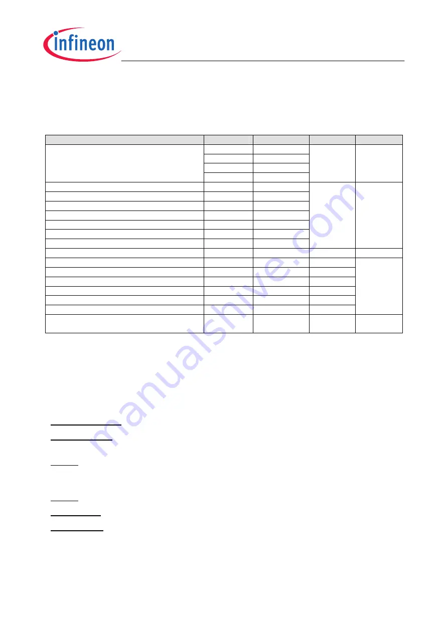
Table  2  indicates  the  configuration  for  all  the  XC164CM  pins  utilized  in  this  UPS 

reference design. 

Table 2

   XC164CM Pins Configuration 

Functions 

Pin Name 

Pin Number 

Direction 

Modules 

CC60 

49 

COUT60 

50 

CC61 

51 

PWM drive signals for inverter 

COUT61 

52 

Out 

CAPCOM6 

Primary current 

AN0 

IGBT temperature 

AN1 

10 

Output current 

AN2 

11 

DC-bus voltage 

AN3 

12 

Output voltage 

AN4 

13 

Line voltage 

AN5 

14 

Battery voltage 

AN10 

15 

In 

ADC 

Line voltage zero-crossing signal 

CC22 

56 

In 

CAPCOM2 

TRIAC control 

P1H.0 

In 

Bypass relay control 

P1L.4 

53 

Out 

DC-bus relay control 

P1L.5 

54 

Out 

Changer control 

P3.8 

35 

Out 

Short-circuit signal 

P9.1 

44 

In 

Disable inverter signal 

P9.2 

45 

Out 

I/O Ports 

UART  communication  with  XC866  for 
display control 

TXD0 

37 

Out 

ASC0 

4.3 

Initialization Settings 

4.3.1 

CAPCOM6 

The CAPCOM6 initialization for PWM signal generation to drive the full-bridge inverter is 

summarized as follows (according to display order in DAvE): 

“Module Clock”:

    Enable module. 

“Pin  Control”:

     Use pin  CC60,  CC61,  COUT60,  COUT61  as  output.  Pin  CC62  is  not 

used. 

“T12”:

        fcpu/1  (Resolution:  0.025us),  Center-aligned  mode,  T12  period  50us  (carried 

frequency 20KHz), Enable interrupt for T12 period match (generating interrupt 
per carrier cycle), Dead-time 1.2us. 

“T13”:

            No initialization is required for it isn’t used here. 

“Multi Ch.”:

   Disable multi-channel mode. 

“Channels”:

  Compare  and  capture  modes  should  be  disabled  for  channel  2.  Channel 

0,1  should  be  individually  configured  as  (x=0,1):  Compare  Mode  3  (Use 
pins  CC6x/COUT6x  as  output);  Enable  T12  modulation  for  CC6x;  The 
compare  output  CC6x  drives    passive  level  while  CC6xST  is  “1”;  The 
compare  output  COUT6x  drives    passive  level  while  CC6xST  is  “0”;  The 
passive  level  of  CC6x  and  COUT6x  output  are  all  “0”;  Enable  dead  time 
generation. 

Содержание XC164 Series

Страница 1: ...Microcontrollers XC164 Main Control for 5KVA Single Phase On Line UPS Reference Design with XC164CM Application Note V1 0 Mar 2007 AP16098...

Страница 2: ...MATION GIVEN IN THIS APPLICATION NOTE Information For further information on technology delivery terms and conditions and prices please contact your nearest Infineon Technologies Office www infineon c...

Страница 3: ...cts major changes since last revision We Listen to Your Comments Any information within this document that you feel is wrong unclear or missing at all Your feedback will help us to continuously improv...

Страница 4: ...3 Main Control Principle 9 4 XC164CS Implementation for Main Control 11 4 1 XC164CM Introduction 11 4 2 Pin Configuration 12 4 3 Initialization Settings 13 4 3 1 CAPCOM6 13 4 3 2 ADC 14 4 3 3 CAPCOM2...

Страница 5: ...e The basic theory and system control flow of this UPS reference design is briefly introduced in Section 2 Section 3 gives the detailed explanation of the main control principle In Section 4 XC164CM i...

Страница 6: ...tion output voltage feedback control system faults and errors managing charger module control modules synchronization is all handled by the control board based on Infineon 16 bit microcontroller XC164...

Страница 7: ...ugh a diode If input line power blackout happens the battery module will be switched to offer power to the inverter in order to keep the power uninterrupted The full bridge inverter is utilized whose...

Страница 8: ...C 187V 253V Input Frequency Nominal Frequency 50Hz 60Hz Auto detection Input Efficiency 87 At rated load VA Watt 5000VA 4000W Nominal Voltage AC 220V Sine Wave Voltage Regulation 2 THD 0 55 Normal mod...

Страница 9: ...rocessed by the microcontroller Once receiving fatal fault signals such as short circuit of the inverter or over temperature of IGBTs the microcontroller will immediately close off all PWM output and...

Страница 10: ...phase with the output voltage phase The ON OFF control signals for DC bus relay and bypass relay along with TRIAC control signal are both produced by the microcontroller The display control board is d...

Страница 11: ...r they can jointly generate control signal patterns to drive AC motors or inverters Its block diagram is shown on Figure 6 ADC Four conversion modes are supported Fixed Channel Single Conversion mode...

Страница 12: ...supports full duplex asynchronous communication and half duplex synchronous communication The highlighted features include Loopback capability autobaud detection unit for asynchronous operating modes...

Страница 13: ...XC866 for display control TXD0 37 Out ASC0 4 3 Initialization Settings 4 3 1 CAPCOM6 The CAPCOM6 initialization for PWM signal generation to drive the full bridge inverter is summarized as follows acc...

Страница 14: ...onnect all digital input stages from port P5 Functions In Initialization Function select ADC_vInit In Function Library Part 1 select ADC_vStartConv ADC_uwReadConv 4 3 3 CAPCOM2 The CAPCOM2 initializat...

Страница 15: ...so the primary current and output voltage are both involved to control the inverter Figure 8 shows the block diagram of this control scheme R LS LRCS RCS 2 1 1 RCS R Figure 8 Dual loop Control Block D...

Страница 16: ...order to be limited within the output range of voltage loop The value of the 90 point of modulated sine wave is also detected in the T12 period match interrupt service routine If short circuit fault o...

Страница 17: ...Control Application Note 17 V1 0 2007 03 4 5 States Diagram and Flow Chart Figure 9 States Diagram for Main Control Figure 9 illustrates the state diagram for main control The flowchart for T12 perio...

Страница 18: ...onize the Line Frequency PI Regulating for Output Voltage A D Conversion for Primary Current Yes Soft Start Yes Disable Inverter Yes Calculate Current Loop Calculate SPWM Duty Cycle Calculate Line Vol...

Страница 19: ...y The waveform for dynamic performance under battery mode is shown in Figure 12 b a Line Mode No Battery b Battery Mode Figure 12 Output Transient Response Figure 13 illustrates the short circuit prot...

Страница 20: ...AP16098 UPS Main Control Experiment Results Application Note 20 V1 0 2007 03 Figure 13 Short Circuit Protection Figure 14 Synchronization Figure 15 Overload Protection and Bypass Control...

Страница 21: ...t structure and difficulty in debugging the current trend for UPS design is to adopt a microcontroller as a main control center instead of the analog solution This application note intends to provide...

Страница 22: ...http www infineon com Published by Infineon Technologies AG...

Отзывы: