Appendix 1 - Technical Reference
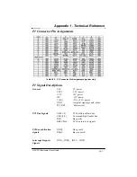
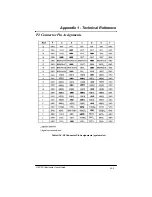
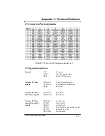
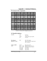
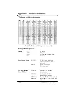
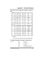
P3 Connector Pin Assignments
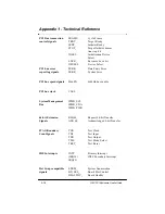
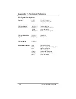
P3 Signal Descriptions
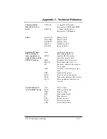
General
VCC
5V power
GND
to digital ground plane
PRST_
Primary PCI bus reset
Primary PCI bus
PAD(31:0)
32-bit Address/Data bus
signals
PCBE(3:0)_
Command/Byte Enable bus
PPAR
Bus parity
Primary PCI bus
PGNT(6:0)_
Bus grants
arbitrations signals
PREQ(6:0)_
Bus requests
Primary PCI bus
PFRAME_
Cycle Frame
transaction control
PTRDY_
Target Ready
signals
PIRDY_
Initiator Ready
PSTOP_
Target/Initiator transaction stop bit
PLOCK_
Resource Lock bit
PDEVSEL_
Devise Select
A1-5
G8 CPCI Enclosure User’s Guide
Table A1-3: P3 Connector Pin Assignments (system slot)
Содержание G8
Страница 1: ...G8 CPCI Enclosure User s Guide G8 8 Slot CompactPCI Enclosure User s Guide 095 30004 00 Rev A ...
Страница 8: ...iv Table of Contents This page was intentionally left blank G8 CPCI Enclosure User s Guide ...
Страница 12: ...1 4 Chapter 1 Introduction G8 CPCI Enclosure User s Guide This page was intentionally left blank ...
Страница 20: ...2 8 G8 CPCI Enclosure User s Guide Chapter 2 Hardware This page was intentionally left blank ...
Страница 26: ...4 4 This page was intentionally left blank Chapter 4 Drive Bays G8 CPCI Enclosure User s Guide ...

