Holtek BC45B4523 Скачать руководство пользователя страница 16

Rev. 1.20

16

October 28, 2020

BC45B4523

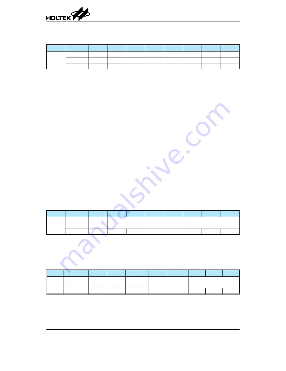
•  PrimaryStatus Register

This register contains flags for indicating the status of modem, interrupt and FIFO.

Address

Bit

7

6

5

4

3

2

1

0

0x03

Name

ModemState[2:0]

IRQ

ERR

HiAlert

LoAlert

Type

R

R

R

R

R

Reset Value

0

0

0

0

1

0

1

Bit 7 

Unimplemented, read as “0”

Bit 6~4

 ModemState[2:0]

: Indicate the state of RX, TX and FIFO

000: Idle – No operation, neither the transmitter nor the receiver is in operation

001: TxSOF – The transmitter is transmitting “Start of Frame” pattern
010: TxData – The transmitter is transmitting data from FIFO or CRC
011: TxEOF – The transmitter is transmitting “End of Frame” pattern

100: RxPrepare – Receiver circuitry is initialized at this state and wait for time period defined by the 

RxWait and BitPhase bits before starting to receive data

101: RxAwaiting – The receiver starts and is waiting for RX Start of Frame from tag
110: Receiving – The receiver is receiving data

Bit 3

 IRQ

: Interrupt request indication

If there are one or more interrupt requests in InterruptFlag register, the IRQ flag will be set to 1.

Bit 2

 ERR

: Error indication

If one or more errors occur in the Error register (Sector0-0x0A), the ERR flag will be set to 1.

Bit 1

 HiAlert

: FIFO HiAlert warning flag

If FIFOLength ≥ 64-Waterlevel, the HiAlert flag will be set to 1.

Bit 0

 LoAlert

: FIFO LoAlert warning flag

If FIFOLength ≤ Waterlevel, the LoAlert flag will be set to 1.

•  FIFOLength Register

This register indicates the number of data remaining in the FIFO buffer.

Address

Bit

7

6

5

4

3

2

1

0

0x04

Name

FIFOLength[6:0]

Type

R

Reset Value

0

0

0

0

0

0

0

Bit 7 

Unimplement, read as “0”

Bit 6~0

 FIFOLength[6:0]

: Indicates the number of data remaining in the FIFO buffer

•  SecondaryStatus Register

This register contains the status flags and values related to timers, CRC and receiver status.

Address

Bit

7

6

5

4

3

2

1

0

0x05

Name

Trunning RF_Det CRCReady EMD_Det SubC_Det

RxLastBit[2:0]

Type

R

R

R

R

R

R

Reset Value

0

0

1

0

0

0

0

0

Bit 7

 Trunning

: Timer running state indication

If Timer is running, Trunning will be set to 1. The value in TimerValue register decreases at the rate of 

timer clock, prescaling from 13.56MHz by TPreScaler bit field.

Содержание BC45B4523

Страница 1: ...em Abbreviation AGC Automatic gain control CRC Cyclic redundancy check DPLL Digital Phase locked Loop EGT Extra guard time in ISO14443B EOF End of Frame ETU Elementary Time Unit fc Carrier frequency F...

Страница 2: ...various configurations e g differential driving single ended driving and a mode to drive an external Class E amplifier for improving the drive strength in the gate antenna setup The BC45B4523 contains...

Страница 3: ...igital I O power supply 8 D_VSS Power Digital and digital I O ground 9 D_VDD Power Digital core power supply need an external 100nF decoupling capacitor 10 RSTPD Digital Input Master Reset Active High...

Страница 4: ...Temperature Range 40 C to 85 C Storage Temperature Range 65 C to 150 C Junction Temperature 125 C Thermal Impedance JA Note QFN 4 4 34 04 C W Note JA is determined by JEDEC 2S2P 4L PCB size 76 2 114...

Страница 5: ...25 C 11 0 A Standby bit StandBy 1 1 0 1 4 mA Average at Wake Up Card Detection Mode TwkUp 500ms transmitter on periodically calculated 10 4 A Average at Wake Up Card Detection Mode TwkUp 1000ms transm...

Страница 6: ...Gain Measured from RX to the output of the internal last amplifier Gain 1 0 11 Gain_ST3 2 0 000 48 dB Gain 1 0 00 Gain_ST3 2 0 000 12 Gstep Gain Step AGCEn 1 3 dB AGCEn 0 Defined by Gain 1 0 12 RxNois...

Страница 7: ...n Max Unit tSCK1 NCS Low to 1st SCK High 12 ns tSCK2 Last SCK Low to NCS High 12 ns tSCKH SCK High Period 25 ns tSCKL SCK Low Period 25 ns tSCKDin Data Change to SCK High 12 ns tSCKDout SCK Low to Dat...

Страница 8: ...opologies The envelope of the input signal is filtered and amplified with optional control by an automatic gain control AGC resulting in an amplitude control to prevent shape distortion The BPSK bit d...

Страница 9: ...100nF 10 F Bea d 5 0 V from USB Power Typical Operating Circuit for External Power Supply Not Apply On Chip 3 3V Regulator BC45B4523 TX1 TX2 RX VMID XTAL1 XTAL2 27 12MHz VREG_IN T_VDD 100nF 100nF 10 F...

Страница 10: ...the table below The timing constrain is shown in SPI Interface Timing diagram presented in the SPI Characteristics section Note that if NCS is set to high MISO will become high impedance This allows...

Страница 11: ...19 20 21 22 23 24 25 26 27 28 29 30 31 32 MISO Hi Z Hi Z D0 7 0 D1 7 0 D2 7 0 SPI Interface for Single Register Multiple Byte Write 0 1 A0 4 0 MOSI SCK NCS 0 0 0 A1 4 0 0 0 0 A2 4 0 0 0 0 0 1 2 3 4 5...

Страница 12: ...ister Name Bit 7 6 5 4 3 2 1 0 Command and Status 0 0 0 Sector Select Sector 0 1 Command Command 7 0 0 2 FIFOData FIFOData 7 0 0 3 PrimaryStatus ModemState 2 0 IRQ ERR HiAlert LoAlert 0 4 FIFOLength F...

Страница 13: ...l Reserved WkCDGoActive WkIgnoreFD WkFDEn Reserved CDTxDelay CDAverage 1 0 3 2 FDThreshold_I_H FDThreshold_I_H 7 0 3 3 FDThreshold_Q_H FDThreshold_Q_H 7 0 3 4 CDThreshold_I_L CDThreshold_I_L 7 0 3 5 C...

Страница 14: ...CfgFall 5 0 1 3 TxCfgRise TxCfgRise 5 0 1 4 1 5 1 6 1 7 3 1 8 1 9 1 A 1 B 1 C 1 D 1 E 1 F 4 2 0 2 1 2 2 2 3 2 4 2 5 2 6 2 7 RX Amplifier Corner 5 2 8 2 9 2 A 2 B 2 C 2 D 2 E ManualFilter M_HP1 1 0 M_L...

Страница 15: ...0x01 Name Command 7 0 Type DY Reset Value 0 0 0 0 0 0 0 0 Bit 7 0 Command 7 0 Commands for the device execution Code Command 0x00 Idle 0x1A Transmit 0x16 Receive 0x1E Transceive 0x12 CalCRC 0x19 LoadK...

Страница 16: ...ne or more interrupt requests in InterruptFlag register the IRQ flag will be set to 1 Bit 2 ERR Error indication If one or more errors occur in the Error register Sector0 0x0A the ERR flag will be set...

Страница 17: ...3 2 1 0 0x06 Name SetIEn CDIEn TimerIEn TxIEn RxIEn IdleIEn HiAlertIEn LoAlertIEn Type W R W R W R W R W R W R W R W Reset Value 0 0 0 0 0 0 0 0 Bit 7 SetIEn Interrupt enable setup SetIEn is a mask bi...

Страница 18: ...refer to the registers in page 5 of Sector 0 for details Bit 4 TxIRq Transmitter interrupt request flag TxIRq is set to 1 when one of these events occurs Transmit Command All data have been transmitte...

Страница 19: ...nication will be encrypted Crypto_MOn is set to 1 only if the authentication process is successful This bit can be cleared by external control Bit 2 TStopNow Timer immediate stop control Setting this...

Страница 20: ...the bit collision position Address Bit 7 6 5 4 3 2 1 0 0x0B Name CollPos 7 0 Type R Reset Value 0 0 0 0 0 0 0 0 Bit 7 0 CollPos 7 0 Collision position 0x00 the bit collision occurs at the start bit 0...

Страница 21: ...mands Bit 3 Unimplemented read as 0 Bit 2 0 TxLastBits 2 0 Define the number of bits of the last byte to be transmitted TxLastBits is used to define the number of bits of the last byte to be transmitt...

Страница 22: ...This register is used to configure TX1 and TX2 output conductance in the modulation state Address Bit 7 6 5 4 3 2 1 0 0x13 Name TxCfgMod Type R W Reset Value 0 1 0 0 0 0 Bit 7 6 Unimplemented read as...

Страница 23: ...Value 0 0 0 0 1 1 1 1 Bit 7 0 ModWidth 7 0 Define the pulse width of the modulation pulse in the transmitted bit Modulation width 2 ModWidth 1 fc For example ISO14443A 106k 0x0F Modulation width 2 36...

Страница 24: ...U low and 3 ETU high 10 11 ETU low and 2 ETU high 11 11 ETU low and 3 ETU high Sector 0 Page 3 RX and Decoder RxControl1 Register This register is used to control the receiver behaviours Address Bit 7...

Страница 25: ...lue defined by CollMarkVal This feature helps resolving anti collision procedure for ISO14443A Bit5 ZeroAfterColl If this bit is set to 1 all received bits after the collided bit will be marked to zer...

Страница 26: ...to be reached by the weaker half bit of the Manchester and FSK coded signal to generate the bit collision which is relative to the amplitude of the stronger half bit 8 steps in design 000 1 9 of stron...

Страница 27: ...it 7 6 5 4 3 2 1 0 0x1E Name Cont_Int RxAutoPD Reserved ByPassEnv Reserved DecoderSrc Type R W R W R W R W R W R W Reset Value 0 1 0 0 0 1 Bit 7 Cont_Int 0 The correlator gain equals to 1 1 The correl...

Страница 28: ...e invalid bits system will continue to search for next valid SOF and will be still in Receiving state If it is cleared to 0 system will quit the Receiving state with error reporting this occurrence Th...

Страница 29: ...trol1 register For example in ISO14443A 106kbps the RxWait should be set to 0x06 ChannelRedundancy Register This register is used to setup the CRC and Parity check for receiving data Address Bit 7 6 5...

Страница 30: ...4 3 2 1 0 0x25 Name ADC_Delay 1 0 FD_MinLvl ADC_FastMode ADC_Rsln Reserved Type R W R W R W R W R W Reset Value 1 0 0 0 1 1 Bit 7 6 Unimplemented read as 0 Bit 5 4 ADC_Delay 1 0 Define ADC delay time...

Страница 31: ...ase quadrature phase of reference clock Address Bit 7 6 5 4 3 2 1 0 0x27 Name ADC_Result_Q 7 0 Type R Reset Value 0 0 0 0 0 0 0 0 Bit 7 0 ADC_Result_Q 7 0 ADC Conversion output Q phase which defines R...

Страница 32: ...estarts from TReloadValue Bit 0 TStartTxBegin 0 The transmission of the 1st valid bit does not affect the timer 1 The program timer starts automatically after the 1st valid bit is transmitted If the p...

Страница 33: ...2 1 0 0x2E Name WkTReloadValue 7 0 Type R W Reset Value 0 0 1 0 0 0 0 0 Bit 7 0 WkTReloadValue 7 0 Define the wake up timer start value Note that the value modification will affect the timer in the ne...

Страница 34: ...in WkUpCD mode when WkFDEn 1 and RxIRq 1 0 If external RF field is detected RxIRq will be set The device will skip Card Detection operation to prevent RF field collision 1 Card Detection operation sti...

Страница 35: ...d_I_H CDIRq will be set when condition is matched following CDIRqCfg CDThreshold_I_H Register This register is used to setup the high threshold level phase I for card detection operation Address Bit 7...

Страница 36: ...and RX Adjustment TDIRqCtrl Register This register is used for TD and IRQ pin control Address Bit 7 6 5 4 3 2 1 0 0x39 Name IO1_InValue IO0_InValue TDSelect IO1_Mode IO0_Mode IRqInv Type R R R W R W R...

Страница 37: ...nternal setting this bit must be fixed at 1 and can not be modified Bit 6 5 RxCorrIntTime 1 0 00 60fc 01 56fc 1x 52fc This bit field is used to adjust integration time of half bit evaluation in correl...

Страница 38: ...egister This register is used to setup the gain of the last state amplifier Address Bit 7 6 5 4 3 2 1 0 0x3F Name Reserved Gain_ST3 2 0 Reserved Type R W R W R W Reset Value 0 0 0 0 0 0 0 0 Bit 7 6 Re...

Страница 39: ...ster This register is used to define LFO trimming methodology Address Bit 7 6 5 4 3 2 1 0 0x03 Name Reserved ManLFOTrim Type R W R W Reset Value 0 0 0 0 0 Bit 7 4 Reserved bits for internal setting th...

Страница 40: ...01 1 02 Vp 4 0mV per step at 8 bits resolution 10 1 64 Vp 6 6mV per step at 8 bits resolution 11 2 01 Vp 7 9mV per step at 8 bits resolution This bit field defines the maximum input RF amplitude at p...

Страница 41: ...is used to control the TX waveform for falling edge Refer to the TX Overshoot Control section for more details Address Bit 7 6 5 4 3 2 1 0 0x10 Name TxOvsT1Fall 3 0 TxOvsT2Fall 3 0 Type R W R W Reset...

Страница 42: ...W Reset Value 0 1 0 0 0 0 Bit 7 6 Unimplemented read as 0 Bit 5 0 TxCfgRise 5 0 Define TX1 and TX2 output conductance at rising edge of TX envelope Sector 1 Page 5 RX Amplifier Corner ManualFilter Reg...

Страница 43: ..._Coef 3 0 Define the filter corner frequency 0000 The corner frequency is set to the highest adjustable value 1111 The corner frequency is set to the lowest adjustable value 0101 Default value Sector...

Страница 44: ...4 0x02 0x02 0x02 0x02 0x02 0x02 0x02 0x02 TBD TBD 0x04 TBD TBD 1 E RxControl2 0x41 0x41 0x41 0x41 0x41 0x41 0x41 0x41 0x41 0x41 0x41 0x41 0x41 0x41 1 F RxControl3 0xA0 0xC3 TBD TBD TBD 0XC3 TBD TBD TB...

Страница 45: ...o the oscillator input the XTAL1 pin Transmitter A transmitter consists of two drivers and a control logic The drivers are capable of operating from 2 7V to 5 5V supplied on the T_VDD pin separated fr...

Страница 46: ...0ASK Tx2Inv Tx2Cw Tx2RFEn Tx1RFEn Type R W R W R W R W R W R W R W Reset Value 0 0 0 1 1 0 0 0 Configuration Input ENV_Int Output Mode Tx1RFEn 100ASK Tx1Inv TX1 Logic TX1 Conductance 0 X 0 0 0 Short t...

Страница 47: ...o transmit data from an internal coder an external control signal via pin TD or a tri state set through the ModulatorSource bit The output driver incorporates a non overlapping clock to reduce the pow...

Страница 48: ...or0 0x14 The following table shows CoderControl settings for ISO14443A ISO14443B and ISO15693 In addition the RF modulation width in both transmitted bits and the SOF in ISO14443A and ISO15693 can be...

Страница 49: ...en conductance is cleared or set to the same value of the first phase and wait until ENV is toggled high When ENV is set high TX conductance is set to the value of the TxCfgCW bit field for a time con...

Страница 50: ...xample Waveform for Overshoot Control 100ASK 1 TxOvsT1Fall 0 TxOvsT2Fall 4 TxOvsT1Rise 0 TxOvsT2Rise 3 ENV TX TxOvsT1Fall TxOvsT2Fall TxOvsT1Rise TxOvsT2Rise TxCfgCW TxCfg Fall TxCfgRise TxCfgCW TxCfg...

Страница 51: ...value Sector0 0x11 directly controls transmitter RF is turned on when register is configured to a proper value as shown in the above Suggested Values and Applications for Transmitter Configuration Co...

Страница 52: ...e internal envelope detector is suitable for proximity readers In addition the architecture allows the device to use an external envelope detector to boost read range In this case the ByPassEnv bit Se...

Страница 53: ...leared to 0 the time constant of the loop bandwidth equals one period of the operating subcarrier If TauAGC is 1 the time constant equals two periods In normal condition clearing the TauAGC to 0 is re...

Страница 54: ...correlator is suitable for high jitter baseband signal where bit boundary must swing around normal bit grid This method monitors repetitiveness of data stream to evaluate the incoming bit whether it i...

Страница 55: ...0x1A 4 3 and SubCCarrier the frame decoder extracts byte data checks CRC parity and frame formats Moreover it removes headers and trailers Then the decoded data is transferred to the FIFO For Manchest...

Страница 56: ...ecommended Values for RxWait and BitPhase in Each Standard table In addition if the control signal RxAutoPD Sector0 0x1E 6 is set the receiver part is only turned on after the end of the transmission...

Страница 57: ...esponse timing among various card manufacturers To achieve highest performance in a certain system or for a specific card RxWait and BitPhase shall be tuned to properly align with the card response Re...

Страница 58: ...difference between RF at input and clock reference as shown in the following figure Then both signals will be filtered to DC voltage represented RF amplitude before being converted to digital domain...

Страница 59: ...ed into field The other is process in which transmitter is turned off and ADC data is calculated After the conversion is completed IdleIRq is set And if the value of register ADC_Result_I Sector0 0x26...

Страница 60: ...CardDetect mode is controlled by CDAverage bits Sector0 0x31 1 0 While FDAverage bits Sector0 0x30 1 0 defines average times for FieldDetect Mode The average configuration is shown in the following ta...

Страница 61: ...Sector1 0x05 1 0 Define maximum input RF amplitude at pin RX for ADC Read Write 00 FD_MinLvl Sector0 0x25 3 Define step size of ADC in Field Detection operation Read Write 0 ADC_Delay Sector0 0x25 5 4...

Страница 62: ...st reading received data from FIFO can be performed immediately after a single byte of data becomes available Functions of registers associated with the FIFO are listed as below Register Address Bit I...

Страница 63: ...s interrupt to an executing command For example when the device is in the receiving state the FIFO is being written by the internal the microcontroller cannot write data to the FIFO Otherwise such rea...

Страница 64: ...t field Sector0 0x2A 4 0 in a range from 0 to 21 and defined as shown in the relation below Tclk 2TPreScaler 13 56MHz When the counter is started from defined events the TReloadValue Sector0 0x2C is i...

Страница 65: ...ion beginning 1st valid bit from uplink is received Reception end End of frame of uplink telegram is received or Error occurs during receiving Definitions of Beginning and End in the Transmission and...

Страница 66: ...controlled by WkTPreScaler bit field Secter0 0x2D 3 0 When the counter is started from writing WkTStartNow bit Secter0 0x2D 7 the WkTReloadValue Secter0 0x2E is initialized to counter Once the wake u...

Страница 67: ...an detect the first clock signal for the clock stable period before leaving this mode The device will completely leave the Soft Power Down mode if PowerDown where the external microcontroller can moni...

Страница 68: ...ield is occurred RxIRq is set and system will go to Sleep phase immediately On the other side if external RF level is lower than set FDThreshold CardDetect mode is executed After CardDetect mode is fi...

Страница 69: ...nt to create TimerIRq flag Read Write 0110 Registers Associated with the WkUpCD Mode Interrupt System The device is comprised of seven sources of interrupts available to serve interrupt oriented progr...

Страница 70: ...FDThreshold_H Turn off RF to avoid RF collision IdleIRq Operation of command is finished and state is changed to idle End of operation of all commands causes IdleIRq set to 1 Setting power down or st...

Страница 71: ...drop in voltage and current passing through This amount of heat must be taken into account for heat dissipation design BC45B4523 VREG_IN VREG_OUT A_VDD IO_VDD D_VSS A_VSS 100nF MCU 3 3V 100nF 10 F VDD...

Страница 72: ...rupt Flag 0x30 Indicate external microcontroller that the device is in initializing state The Startup command is started by the internal state machine automatically after reset It is used to indicate...

Страница 73: ...m If no more data available in the FIFO the CODEC appends CRC and EOF at the end and switches to idle state The state machine leaves the transmission state to idle state and the TxIRq and IdleIRq flag...

Страница 74: ...ent1Pulse In ISO15693 there is a requirement to send a single RF gap on air to indicate next slot during anti collision Regardless of data in the FIFO setting bit Sent1Pulse Sector0 0x14 7 and then wr...

Страница 75: ...n has finished is the second part of Transceive command After executing the Receive command from SPI the CODEC state machine changes to RxPrepare state and delays start of the receiver by the number o...

Страница 76: ...o the FIFO and the bit CRCErr in the Error register Sector0 0x0A will be set In case of parity if the bit ParityEn is set in the ChannelRedundancy register the parity is expected after the end of each...

Страница 77: ...of reception some errors in reception are indicated via the error flags in the Error register The meaning of the error flags related to the reception is described as follows Error Flag Event FramingE...

Страница 78: ...n ISO14443A Dynamic 000 SubCPulses Sector0 0x19 7 5 Define the number of subcarrier pulses per bit Read Write 011 SubCCarrier Sector0 0x19 4 3 Define the number of carrier clocks used in subcarrier Re...

Страница 79: ...rite 00 SOFSel43A Sector0 0x3C 3 Define the method of ISO1444A Manchester pattern header recognition Read Write 1 Gain_ST3 Sector0 0x3F 5 3 Define gain of the last state amplifier for systems requirin...

Страница 80: ...activates the CRC calculation of the data stream in the FIFO The preset value is defined in registers CRCPresetMSB and CRCPresetLSB and the calculation algorithm is configured by the ChannelRedundanc...

Страница 81: ...ead from FIFO Interrupt Flag 0x1C Execute the authentication between reader and card Card s Authent command Card s Block address Card s UID LSB Card s UID MSB IdleIRq TxIRq RxIRq The Authent command e...

Страница 82: ...brate ADC to record the ADC offset value IdleIrq The ADCCalibrate command enables ADC calibration process This command will start ADC conversion without input signal by disabling transmitter The ADC r...

Страница 83: ...transmitter is set to drive a differential antenna from pin TX1 and TX2 and the internal envelope detector is employed L1 C1 C2 and C3 form a transmitter antenna matching network while LAnt is a loop...

Страница 84: ...Moreover the device is capable of connecting to various RF topologies The transmitter driver can be designed to connect to not only a differential drive antenna but also a single ended drive antenna a...

Страница 85: ...o the carrier dividing scheme Note that the ByPassENV bit must be set if the external envelope detector is used A simple external envelope detector connection is shown in the following figure For an o...

Страница 86: ...g part and the digital part digital section of the device and the external microcontroller can be on the same ground plane However the power source direction and the ground return path from such noisy...

Страница 87: ...Rev 1 20 87 October 28 2020 BC45B4523 OUT3P RESET_INT RX OUT3P and RESET_INT Test Register is Set to 0x10 VRECT CORR_S_VALID RX VRECT and CORR_S_VALID Test Register is Set to 0x1E...

Страница 88: ...and ISO14443B the Twait must be set to assert before SOF of the card response Also some test signals can be used to see phase distortion from the antenna and its effect The following OUT3P and BPSK_DA...

Страница 89: ...Rev 1 20 89 October 28 2020 BC45B4523 OUT3P BPSK_DATA RX OUT3P and BPSK_DATA Test Register is Set to 0x11 OUT3P S_VALID RX OUT3P and S_VALID Test Register is Set to 0x12...

Страница 90: ...t Register is Set to 0x13 Furthermore when the proprietary protocol is implemented external MCU need to decode baseband itself by probling out RAW_DATA as shown in the following figures OUT3N RAW_DATA...

Страница 91: ...oder 0x1E 0 CORR_S_VALID Manch FSK decoder VRECT Manch FSK decoder 0x1F 0 CORR_S_COLL Manch FSK decoder VRECT Manch FSK decoder 0x4D 0 TX_EN Transmitter VRECT Manch FSK decoder Key Test Signal and Ind...

Страница 92: ...inking current can be approximated to be half sinusoidal shape as illustrated in the following figure Therefore the power loss from voltage drop across the driver is PlossTX Iout 2 Rout Where the Iout...

Страница 93: ...2 5 0 312W For the regulator the loss is PReg 150mA 5V 3 3V 0 255W The temperature coefficient JA of an operating PCB is 34 C W As shown in the Absolute Maximum Rating The different temperature betwee...

Страница 94: ...users are reminded to consult the Holtek website for the latest version of the package information Additional supplementary information with regard to packaging is listed below Click on the relevant...

Страница 95: ...0 035 A1 0 000 0 001 0 002 A3 0 008 BSC b 0 007 0 010 0 012 D 0 157 BSC E 0 157 BSC e 0 020 BSC D2 0 104 0 106 0 108 E2 0 104 0 106 0 108 L 0 014 0 016 0 018 Symbol Dimensions in mm Min Nom Max A 0 80...

Страница 96: ...e purpose of illustration and Holtek makes no warranty or representation that such applications will be suitable without further modification nor recommends the use of its products for application tha...

Отзывы: