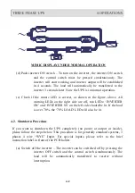
(d) Close the bypass breaker – The reserve breaker and reserve static switch
are still conducting. Therefore, when the maintenance bypass
breaker is closed, power will flow through the bypass loop instead
of the reserve loop because of the lower impedance of bypass
loop.
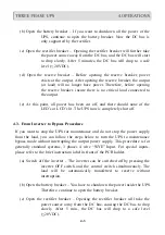
(e) Open the reserve breaker – You can now open the reserve breaker to free
the UPS from any power supply.
4.4. From Bypass to Inverter Procedure
If the UPS is in maintenance bypass mode, and you want to turn the UPS to
normal mode without interrupting the output AC, please follow the steps below.
This procedure is for generally standard systems, 3 phases 4 wire “WYE” Input.
For special inputs, please refer to the brief instruction label in front of the PCB
holder.
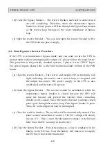
(a) Close the reserve breaker – The reserve and output LED on the mimic will
light, indicating the reserve static switch loop is energized, and
the output has power. The power supply in the UPS is also
established, and the fans will operate.
(b) Open the bypass breaker – The inverter cannot be switched on while the
maintenance bypass breaker is closed (because the CPU will
sense the breaker and prevent the inverter from connecting
directly to AC source). Since the reserve breaker is already closed,
power goes through the reserve loop if the bypass breaker is open.
Thus, AC at the output will not be interrupted.
(c) Close the rectifier breaker - The rectifier will be automatically started if the
power source connection is correct. The DC voltage will slowly
rise up (15 – 30sec.) until the designated voltage is reached and
held. Now, the DC is ready for the inverter.
(d) Close the battery breaker – For safety purposes, a fuse is employed in the
battery to the DC bus. Now the battery will take-over to supply
the DC bus if the rectifier mains fail.
4-4
Содержание T3UPS-33-700K
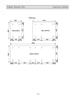
Страница 18: ...1 7 Dimension Drawings 10KVA 60KVA OUTLINE DRAWING 1 13 ...
Страница 19: ...10KVA 60KVA INTERIOR DRAWING 1 14 ...
Страница 20: ...75KVA 160KVA OUTLINE DRAWING 1 15 ...
Страница 21: ...75KVA 160KVA INTERIOR DRAWING 1 16 ...
Страница 22: ...175KVA 320KVA OUTLINE DRAWING 1 17 ...
Страница 23: ...175KVA 320KVA INTERIOR DRAWING 1 18 ...
Страница 24: ...INTER PCB DIAGRAM 1 19 ...
Страница 31: ...1 ...
Страница 35: ...3 3 ...
Страница 70: ...ONE TO TWO SERIAL REDUNDANCY 8 3 ...
Страница 77: ...Appendices Additional Data on Options UPSCOMTM UPSCALLTM DCMANTM ...
Страница 80: ...3 ...
Страница 81: ......

