background image

Содержание MBM-530NS

Страница 1: ...MBM 530NS User s Manual...

Страница 2: ...of Intel Corporation Windows and MS DOS are registered trademarks of Microsoft Corporation Award is a registered trademark of Award Software International Inc IBM and PS 2 are trademarks of Internati...

Страница 3: ...eturn it to the manufacturer for repairing Products warranty or service will not be extended if 1 the product is repaired modified or altered unless such repair modification or alternation is authoriz...

Страница 4: ...4 MBM 530NS User s Manual...

Страница 5: ...Taiwan 235 Telephone 886 2 3234 7000 Fax 886 2 2226 9623 E mail ipcservice nfic com tw Formosa USA Inc Address 21540 Praire Street Unit A Chatsworth CA91311 U S A Telephone 1 818 407 4965 Fax 1 818 4...

Страница 6: ...lel Port 24 2 HARDWARE CONFIGURATION 27 2 1 Jumper Connector Quick Reference Table 28 2 2 Block Diagram 29 2 3 Component Locations 30 2 4 How to Set the Jumper 31 2 5 System Clock Select and CPU Setti...

Страница 7: ...on 62 4 1 1 Award BIOS 62 4 1 2 Entering the Award BIOS Setup Menu 63 4 1 3 BIOS CONFIGURATION 64 4 2 Standard CMOS Setup 67 4 3 BIOS Features Setup 72 4 4 Chipset Features Setup 79 4 5 Power Manageme...

Страница 8: ......

Страница 9: ...ds such as support for four RS 232C ports and one 168 pin DIMM socket for up to 128MB of extended memory SDRAM The unit also comes with a programmable watchdog timer and other standard interfaces The...

Страница 10: ...ng items have been included inside the MBM 530NS package n MBM 530NS all in one single CPU board n Hard disk drive interface cable n Parallel port interface cable n Floppy interface cable n PS 2 mouse...

Страница 11: ...On board CRT and 18 bit TFT LCD panel display n Supports IDE hard disk drives n Supports floppy disk drives n Supports 1 bi directional parallel port n Supports 2 USB port n Supports 16 bit PnP sound...

Страница 12: ......

Страница 13: ...ktop and IPC computer designs The MediaGX MMX enhanced processor companion chips provide advanced video and audio functions and permit direct interface to memory This high performance 64 bit processor...

Страница 14: ...equivalent of two 8237A DMA controllers are implemented on the MBM 530NS board Each controller is a four channel DMA device that will generate the memory addresses and control signals necessary to tra...

Страница 15: ...buffer or wait for the system to poll its status register to determine when data is available Data can be written to the keyboard by writing data to the output buffer of the keyboard controller Each...

Страница 16: ...with the second controller representing IRQ8 to IRQ15 which is rerouted through IRQ2 on the first controller The following is the system information of interrupts levels IRQ8 Real time clock IRQ9 Seri...

Страница 17: ...0F1 Reset Math Co processor 0F8 0FF Math Co processor 170 178 Fixed disk 1 1F0 1F8 Fixed disk 0 201 Game port 208 20A EMS register 0 218 21A EMS register 1 278 27F Parallel printer port 2 LPT 2 2E8 2...

Страница 18: ...Address Description 00 Seconds 01 Second alarm 02 Minutes 03 Minute alarm 04 Hours 05 Hour alarm 06 Day of week 07 Date of month 08 Month 09 Year 0A Status register A 0B Status register B 0C Status r...

Страница 19: ...ach with a timing frequency of 1 19 MHz Timer 0 The output of this timer is tied to interrupt request 0 IRQ 0 Timer 1 This timer is used to trigger memory refresh cycles Timer 2 This timer provides th...

Страница 20: ...16x clock to drive the receiver logic Also included in the ACE a completed MODEM control capability and a processor interrupt system that may be software tailored to the computing time required handli...

Страница 21: ...Bit 7 Must be 0 4 Interrupt Identification Register IIR Bit 0 0 if Interrupt Pending Bit 1 Interrupt ID Bit 0 Bit 2 Interrupt ID Bit 1 Bit 3 Must be 0 Bit 4 Must be 0 Bit 5 Must be 0 Bit 6 Must be 0 B...

Страница 22: ...ror OR Bit 2 Parity Error PE Bit 3 Framing Error FE Bit 4 Break Interrupt BI Bit 5 Transmitter Holding Register Empty THRE Bit 6 Transmitter Shift Register Empty TSRE Bit 7 Must be 0 8 MODEM Status Re...

Страница 23: ...Bit 1 Bit 1 Bit 9 Bit 2 Bit 2 Bit 10 Bit 3 Bit 3 Bit 11 Bit 4 Bit 4 Bit 12 Bit 5 Bit 5 Bit 13 Bit 6 Bit 6 Bit 14 Bit 7 Bit 7 Bit 15 Desired Baud Rate Divisor Used to Generate 16x Clock 300 384 600 19...

Страница 24: ...7309 is for attaching various devices that accept eight bits of parallel data at standard TTL level 3 Data Swapper The system microprocessor can read the contents of the printer s Data Latch through t...

Страница 25: ...eceived the character and is ready to accept another Normally this signal will be active for approximately 5 microseconds before receiving a BUSY message stops Bit 5 A1 means the printer has detected...

Страница 26: ...te only Bit 4 A1 in this position allows an interrupt to occur when ACK changes from low state to high state Bit 3 A1 in this bit position selects the printer Bit 2 A0 starts the printer 50 microsecon...

Страница 27: ...n with your fingers or small needle nosed pliers Place the jumper over the two pins designated for the desired setting Press the jumper evenly onto the pins Be careful not to bend the pins We will sho...

Страница 28: ...tor J4 VGA Connector D SUB J5 IrDA Connector J6 SoDimm RAM Socket J7 COM2 RS 232 422 485 Selection S1 LCD Backlight Control JP1 CMOS Clear JP2 LCD Connector JP3 LCD Power VDD Select JP4 External Reset...

Страница 29: ...LOCK GENERATOR KEYBOARD MOUSE Geode CS5530A FLOPPY IrDA ISA BUS GRAPHICS AND VIDEO VOLTAGE REGULATOR MODULE V R M IDE MAIN MEMORY 144 PIN SODIMM Doc BLOCK DIAGRAM B Monday February 05 2001 20 2 0 1 Ti...

Страница 30: ...ides the hardware s jumper settings the connectors locations and the pin assignments The 1 pin assignments have all been designed on the right side of the board with a block indication on the diagram...

Страница 31: ...close the pins The jumper can be combined into sets which called jumper blocks When the jumpers are all in the block you have to put them together to set up the hardware configuration The figure belo...

Страница 32: ...NS User s Manual 2 5 System Clock Select and CPU Setting Table 1 CPU Core versus Core Frequency Characteristics CPU GX1 Series Core Voltage System Clock Freq Multiplier Core Freq 300B 85 2 0 2 0V 33MH...

Страница 33: ...osa21 com MBM 530NS User s Manual 33 2 6 Jumper Setting J1 Power Connector The J1 is a 4 pin power connector it connects the power 5V and 12V to apply MBM 530NS power 87654321 ON MBM 530 1 2 3 4 1 12V...

Страница 34: ...ual J2 TTL I O TTL Input Demo Program include stdio h include stdlib h include dos h define GPIO20 0x01 GPIO20 87654321 ON MBM 530 1 TTL Output Port 1 2 TTL Output Port 2 3 TTL Input Port 1 4 TTL Inpu...

Страница 35: ...Dev_Index Choose Logical Dev PM outportb Data_Reg PM_Num outportb Index_Reg 0x30 Enable PM register access outportb Data_Reg 0x01 outportb Index_Reg 0x60 PM Base address MSB mBAR inportb Data_Reg out...

Страница 36: ...Index_Reg 0x61 GPIO Base address LSB lBAR inportb Data_Reg GPIOBAR unsigned mBAR 8 unsigned lBAR Read from GPIO20 and check its status outportb Index_Reg 0x22 GPIO Bank select port_Select inportb Dat...

Страница 37: ...Reg 0x002E Data_Reg 0x002F unsigned char Dev_Index 0x07 GPIO_Num 0x07 PM_Num 0x08 unsigned char tmpData void main void unsigned char mBAR lBAR PM_Index_Reg PM_Data_Reg GPIO_En port_Select CFGDAT unsig...

Страница 38: ...rts function enable PM_Data_Reg inportb PMBAR 0x01 outportb PM_Index_Reg 0x01 GPIO_En inportb PM_Data_Reg outportb PM_Index_Reg 0x01 outportb PM_Data_Reg GPIO_En 0x80 outportb Index_Reg Dev_Index Choo...

Страница 39: ...select port_Select inportb Data_Reg outportb Index_Reg 0x22 GPIO port3 select outportb Data_Reg port_Select 0x80 outportb GPIOBAR 0x05 0x80 set port3 output direction tmpData inportb GPIOBAR 0x04 outp...

Страница 40: ...S User s Manual J3 CD Audio in Connector The J3 is used to connect to a multi sound panel connector It consist of a line in a line out and a microphone 87654321 ON MBM 530 1 2 3 4 1 CD In L 2 GND 3 GN...

Страница 41: ...tyle The last connector on the cable is the master Pin Signal Pin Signal 1 33 odd GROUND 18 DIRECTION 2 REDUCED WRITE CURRENT 20 STEP OUTPUT PULSE 4 NOT USED 22 WRITE DATA 6 NOT USED 24 WRITE ENABLE 8...

Страница 42: ...when you are using the on board VGA controller as the display adapter Pin assignments for the J5 connector are as follows 87654321 ON MBM 530 DB1 CRT Connector 6 10 15 11 1 2 3 4 5 1 Red 2 Green 3 Blu...

Страница 43: ...sing the internal IrDA header it will automatically become COM 2 This means that COM 2 will not be able to be used as a serial connection This selection should be selected in the BIOS The best setting...

Страница 44: ...44 MBM 530NS User s Manual JP1 LCD Backlight Control 87654321 ON MBM 530 3 2 1 1 Backlight 2 GND 3 12V Output...

Страница 45: ...Web site www formosa21 com MBM 530NS User s Manual 45 JP2 CMOS Clear 87654321 ON MBM 530 3 2 1 Clear CMOS 3 2 1 Normal...

Страница 46: ...w 87654321 ON MBM 530 1 LCD Power VDD 21 D10 2 GND 22 D11 3 FPCLK 23 LCD Power VDD 4 GND 24 D12 5 GND 25 D13 6 PPHSYNC 26 D14 7 FPVSYNC 27 D15 8 M Signal 28 GND 9 D16 29 D0 10 D17 30 D1 11 NC 31 D2 12...

Страница 47: ...Web site www formosa21 com MBM 530NS User s Manual 47 JP4 LCD Power VDD Select 87654321 ON MBM 530 1 2 3 3 3V 1 2 3 5V...

Страница 48: ...Reset Switch The switch is act as the MBM 530NS system reset control The extra reset control can be done by JP5 which connect to an external reset switch Shorting these two pins will reset the system...

Страница 49: ...Web site www formosa21 com MBM 530NS User s Manual 49 JP6 COM2 Power Select 87654321 ON MBM 530 1 2 3 5V 1 2 3 12V...

Страница 50: ...gure them use the BIOS Setup program covered later section The switch S1 for choosing between RS 232 RS 422 and RS 485 can adjust COM 2 Function 1 2 3 4 5 6 7 8 RS 232 Off Off Off Off Off Off Off Off...

Страница 51: ...Signal CN2 DB 25 Signal 1 1 Strobe 2 14 Auto Form Feed 3 2 Data 0 4 15 Error 5 3 Data 1 6 16 Initialize 7 4 Data 2 8 17 Printer Select In 9 5 Data 3 10 18 Ground 11 6 Data 4 12 19 Ground 13 7 Data 5 1...

Страница 52: ...connector COM1 COM2 uses on board 10 pin pinhead connectors CN3 To configure them use the BIOS Setup program covered later section The switch S1 for choosing between RS 485 RS 422 and RS 232C can adju...

Страница 53: ...eb site www formosa21 com MBM 530NS User s Manual 53 CN4 Multi Sound Panel Connector 87654321 ON MBM 530 1 GND 6 Line In R 2 MIC In 7 Line Out L 3 Line Out R 8 GND 4 GND 9 GND 5 GND 10 Line in L 2 10...

Страница 54: ...illustrates the pin assignments of the hard disk drive s 44 pin connector The last pin on the cable is the master PIN SIGNAL PIN SIGNAL PIN SIGNAL PIN SIGNAL 1 RESET 2 GROUND 23 LOW A 24 GROUND 3 DATA...

Страница 55: ...cation is being written SA0 SA19 Input Output The System Address lines run from bit 0 to 19 They are latched onto the falling edge of BALE DRQ 0 3 5 7 Input DMA Request channels 0 to 3 are for 8 bit d...

Страница 56: ...y are prioritized in the following sequence Highest IRQ 9 10 11 12 13 15 3 4 5 6 7 Lowest MASTER Input The MASTER is the signal from the I O processor which gains control as the master and should be h...

Страница 57: ...DiskOnChip Socket DOC Memory Address Select This section provides the information about how to use the DOC DiskOnChip 1 The address of DiskOnChip is DC000H 2 Insert programmed DiskOnChip into socket...

Страница 58: ......

Страница 59: ...IO DIR cryix exe license pdf RTL8139 DIR Brom DIR Client32 DIR Dmi DIR Freebsd DIR Linux DIR Macos DIR Mslanman dos DIR Mslanman Os2 DIR Ndis2Dos DIR Ndis2Os2 DIR Nt351 DIR Nwclient DIR Nwserver DIR R...

Страница 60: ...Execute the file Cryix exe the system will auto setup the video and audio functions 3 3 Install Network Utility 1 Change directory to the Rtl8139 2 Choose the proper driver for your operating system 3...

Страница 61: ...n n Standard CMOS Features n BIOS Features Setup n Chipset Features Setup n Power Management Setup n PnP PCI Configurations n Load BIOS Defaults n Load Setup Defaults n Integrated Peripherals Features...

Страница 62: ...updated when BIOS upgrades are released This built in routine allows you to configure the system parameters and then save the configuration into the 256 bytes CMOS area in the BIOS ROM The BIOS ROM is...

Страница 63: ...Alt Delete or by pressing the Reset button on the system case You can also restart by turning the system off and then back on again Do it only if the first two methods fail If you do not press the key...

Страница 64: ...PNP PCI configuration This setup page includes all the configurations of PCI PnP ISA resources Load BIOS defaults BIOS Defaults indicates the most appropriate value of the system parameters that syst...

Страница 65: ...exit current page and return to Main Menu PageUp Increase the numeric value or make changes modify parameters PageDown Decrease the numeric value or make change modify parameters Increase the numeric...

Страница 66: ...ion LOAD BIOS DEFAULTS to load the minimum settings for troubleshooting or LOAD SETUP DEFAULTS to load optimised defaults for regular use All applicable set tings will be modified Note All BIOS defaul...

Страница 67: ...CMOS battery weakens It will also get lost when you remove the CMOS battery from SBC Note The screen contents in this manual are provided as examples only and may not reflect the screen contents disp...

Страница 68: ...nth month From Jan to Dec year From 1900 to 2099 Time To set the time highlight the Time field and then press PageUp PageDown or to set the current time Follow the hour minute and second format Valid...

Страница 69: ...sectors and MODE The SIZE field automatically adjusts according to the configuration you specify The documentation that comes with your hard disk should provide you with the information regarding the...

Страница 70: ...f floppy disk drives installed in your system The available options for drive A are 360K 5 25in 1 2M 5 25in 720K 3 5in 1 44M 3 5in 2 88M 3 5in None None No floppy drive installed 360K 5 25 in 5 1 4 in...

Страница 71: ...op for a keyboard or disk error it will stop for all other errors Memory This field is display only The BIOS will automatically detect the total amount of memory during POST Power On Self Test Base Me...

Страница 72: ...f these keys and their respective uses If you need information on a particular entry highlight it and then press F1 A pop up help menu will appear to provide you with the information you need F5 loads...

Страница 73: ...ions which at tempting to access the boot sector table can cause the above warning message If you will be running such a program we recommend that you first disable Virus Warning beforehand CPU Intern...

Страница 74: ...Swap Floppy Drive Disabled This item allows you to switch between the floppy letter assignments without hardware modification The choice Enabled Disabled Boot Up Floppy Seek Enabled During POST BIOS w...

Страница 75: ...lding down a key on the keyboard will generate only one keystroke On the contrary the BIOS will report repeated keystrokes when this field is enabled For example you may use this feature to accelerate...

Страница 76: ...this section this option determines when the system prompts for password It allows you to limit access to the system and Setup or just to Setup The default setting is Setup where the system goes thro...

Страница 77: ...IRQ for VGA Disabled The default value is Disabled Enable Assign a specific IRQ for VGA Disable No IRQ is assigned for VGA OS Select for DRAM 64 Non OS2 This item allows you to access the memory that...

Страница 78: ...system to shadow the ROMs of optional expansion controllers to RAM To enable this feature a specific shadowing address is necessary An example of such ROM shadowing would be the support of onboard SC...

Страница 79: ...ault settings have been chosen because they provide the best operating conditions for your system Warning The parameters in this screen are for system designers service personnel and technically compe...

Страница 80: ...Recovery Time These options specify the length of the delay in BUSCLK inserted between consecutive 8 bit 16 bit I O operations USB Controller Disabled If you do not use the onboard USB feature it all...

Страница 81: ...related to the following modes Doze Mode Standby Mode Suspend Mode HDD Power Down There are three selections for Power Management Min Power Saving Minimum power management Doze Mode 1 hr Standby Mode...

Страница 82: ...tem is in Suspend mode Selecting 1 Min 15 Min allows you define the HDD idle time before the HDD enters the Power Saving Mode The options 1 Min 15 Min will not work concurrently When HDD is in the Pow...

Страница 83: ...trongly recommended that only experienced users should make any changes to the default settings PnP PCI Configuration PnP OS Installed No This field allows you to use a Plug and Play PnP operating sys...

Страница 84: ...Data when you have installed a new add on and the system has participated a serious configuration conflict which causes the operating system to not boot The Choice Enabled and Disabled PCI IRQ Active...

Страница 85: ...anently in the BIOS ROM These BIOS defaults are designed to provide the minimum requirements for the system to operate To load the BIOS defaults highlight Load BIOS Defaults on the main menu and then...

Страница 86: ...lts which is designed to provide maximum system performance To load the Setup defaults highlight Load Setup Defaults on the main menu and then press Enter The system displays a confirmation message on...

Страница 87: ...use the fast block mode to transfer data to and from your hard disk drive HDD Enabled IDE controller uses block mode Disabled IDE controller uses standard mode Primary IDE Channel Enabled The integrat...

Страница 88: ...to Disabled if you want to use a separate controller card to connect the floppy disk drives The Choice Enabled Disabled Onboard Serial Port 1 3F8 IRQ4 Port 2 2F8 IRQ3 These items allow you to determi...

Страница 89: ...rd parallel port Select ECP mode for Microsoft and HP Extended Capabilities Parallel Port Select ECP EPP mode for both ECP and EPP modes The Choice SPP ECP EPP1 7 EPP1 7 SPP EPP1 9 SPP ECP ECP EPP1 9...

Страница 90: ...also press Esc to abort the selection and not enter a password To disable a password just press Enter when you are prompted to enter the password A message will confirm the password will be disabled O...

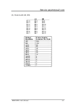
Страница 91: ...Web site www formosa21 com MBM 530NS User s Manual 91 when user tries to enter Setup utility...

Страница 92: ...meters causes the program to enter zeros after that drive letter When auto detection is completed the program automatically enters all entries you accepted on the field for that drive in the Standard...

Страница 93: ...n on the main menu type Y and then press Enter When you confirm the entries and save them the system will automatically reboot and per form the changes you made Save Exit Setup 4 13 Exit Without Save...

Страница 94: ...rompt and then copy AWDFLASH EXE to this diskette 2 Re boot the system and run AWDFLASH EXE from this diskette your screen will show the table below 3 Press Enter for the File Name to Program window 4...

Страница 95: ...Diskette your screen will show the table below 5 5 Enter the new BIOS file name with extension into the File Name to Program window and then press Enter 6 Enter N for the Error Message Do You Want To...

Страница 96: ......

Страница 97: ...set FDD Port Supports 3 5 or 5 25 Floppy Devices Parallel Port Supports SPP EPP ECP Mode COM Port One RS232C One RS232C RS485C with 5V 12V Selected by Jumper IR Port One 115Kbps IrDA Compliant Serial...

Страница 98: ...8 Bit TFT LCD Display Simultaneous Supports LCD Back Light Control Connector LED Indicators Power LED and IDE LED EXT BUS 16 Bit PC 104 BUS and 32 Bit PCI BUS PCI Bus depends on the PCB Size WDT Progr...

Страница 99: ...ut data Step 3 Waiting for data empty Step 4 Disable TXC Note Please refer to the Serial Port section in the chapter System Controller for the detailed description of the COM port s register 1 Initial...

Страница 100: ...signal and the bit 0 of the address of offset 4 sets at 0 3 Send out one block data Transmit the data more than two characters Step 1 Enable the TXC signal and the bit 0 of the address of offset 4 jus...

Страница 101: ...20 OUT H3FC INP H3FC OR H01 30 REM Send out one character 40 PRINT 1 OUTCHR 50 REM Check transmitter holding register and shift register 60 IF INP H3FD AND H60 0 THEN 60 70 REM Disable transmitter by...

Страница 102: ...0 1 0 8 3 0 1 1 16 4 1 0 0 20 5 1 0 1 24 6 1 1 0 28 7 1 1 1 32 WDT I O Port 443H I O Write The enable cycle 443H I O Write The refresh cycle 441H I O Write The disable cycle Sample Program include st...

Страница 103: ...28 32 n exit 1 outportb Index_Reg Dev_Index Choose Logical Dev PM outportb Data_Reg PM_Num outportb Index_Reg 0x30 Enable PM register access outportb Data_Reg 0x01 outportb Index_Reg 0x60 PM Base add...

Страница 104: ...ata_Reg outportb Index_Reg 0x22 GPIO port1 select outportb Data_Reg port_Select 0x7F outportb Index_Reg 0x60 GPIO Base address MSB mBAR inportb Data_Reg outportb Index_Reg 0x61 GPIO Base address LSB l...

Отзывы: