14. How to use
RX4111CE
Jump to
ETM62E-02
Seiko Epson Corporation
48
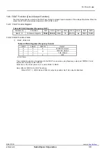
6h
Time Stamp
Control 3
z
z
z
TSFUL
TSEMP TSDA2
TSDA1 TSDA0
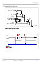
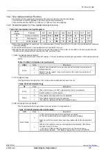
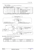
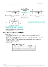
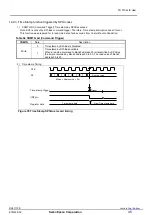
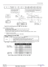
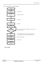
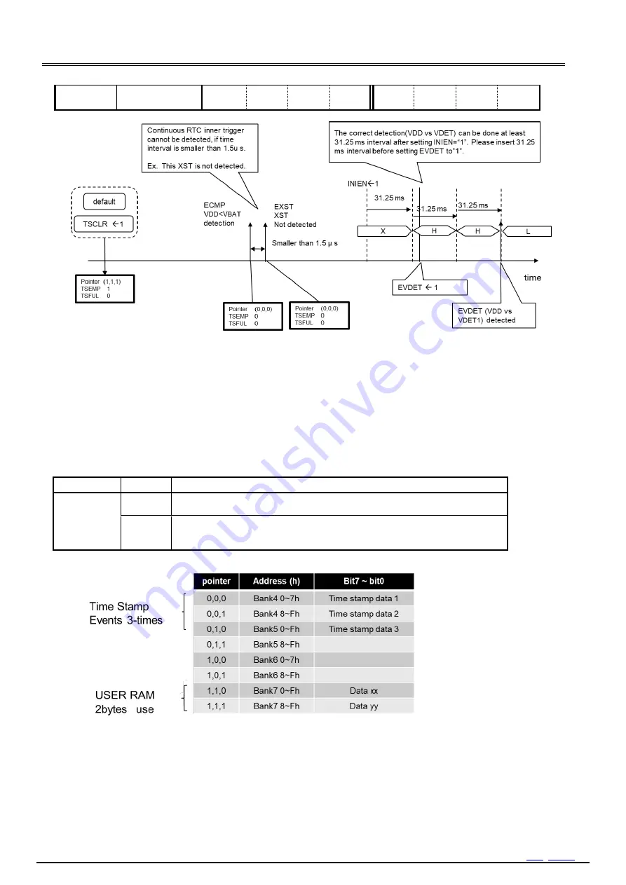
Figure 37 Careful timing process for VDET, XST time stamp
14.8.7. Multiple Time Stamp
By using following registers, user can record time stamp maximum 8-times.
Multiple timestamp related register
Multiple time stamp operation is possible by setting the following registers.
1/1024 seconds and WEEK information are not recorded in the recording area of Bank4
Bank7.
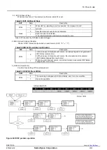
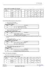
1) TSRAM bit (Time Stamp RAM)
Selection of time stamp recording area or USER RAM.
Table 63 TSRAM bit (Time Stamp RAM)
TSRAM
Data
Description
Write
0
It can read and write as USER RAM.
Time stamp data is recorded only at addresses Bank2 0h to 8h.
1
Bank4 to Bank7 is used as the time stamp recording area.
To clear the time stamp data, write 0 directly to the recording area by SPI-Bus
access.
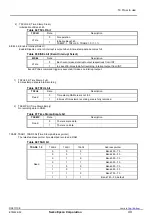
When TSRAM = 1, the first time stamp is recorded in both Bank2 0h
8h and Bank4 0h
7h.
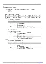
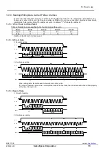
Figure 38 Mixed usage of USER RAM and Time stamp RAM

