67
c
Paper Feed Section
chap.2
¡
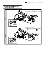
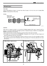
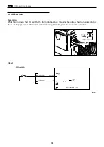
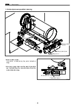
When there is no paper :
¡
When there is paper placed :
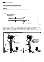
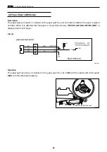
(5) Paper Sensor
Description
Circuits
Operation
Senses presence/absence of paper in the feed tray. When the paper in the tray runs out, the message
"NO
PAPER"
is displayed and printing stops.
When there is no paper, the sensor is in the state of photopassing(open). When paper is placed inside, the
sensor is in the state of photointerrupting(close). When an absence of paper is detected, the message
"NO
PAPER"
is displayed on the LCD panel.
2
When absence of paper is sensed, platemaking, printing and test printing are not possible.
2
If the paper runs out during printing,
"NO PAPER"
is displayed on the LCD panel, printing is stopped, and
the feed tray descends to its lower limit position.
2
If the paper runs out during platemaking, operation continues until the end of the platemaking process,
then operation stops (without proceeding to the printing process), and the feed tray descends to its lower
limit position.
R8S02053
R8S02E19e
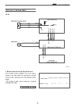
Photointerrupting
Photopassing
Paper
Paper sensor
Содержание DP-S Series
Страница 1: ......
Страница 9: ......
Страница 11: ......
Страница 16: ...x Dimensions chap 1 15 R8S01001 xDimensions 622 1360 510 228 1080 710 980 688 370 mm...
Страница 22: ...v Part Names and Their Functions chap 1 21 44000A1e 2A 2B 2C R8S01006a 2Detailed drawing...
Страница 33: ...32 z Scanner Section chap 2 Circuit R8S02E03e...
Страница 53: ...52 x Platemaking Master Feed Ejection Section chap 2 2 Master Attach Detach Operation R8S02037e...
Страница 87: ...86 m Drum Section chap 2 2 Circuit R8S02E30...
Страница 171: ...170 MEMO...
Страница 193: ...192 MEMO...
Страница 195: ...194 z Help mode List chap 7 z HELP Mode List...
Страница 243: ...242 c HELP Mode Function and Operation Procedures chap 7...
Страница 270: ...269 c HELP Mode Function and Operation Procedures chap 7...
Страница 281: ...280 MEMO...
Страница 293: ...292 z Electrical Parts Layout and Their Functions chap 9 MEMO...
Страница 294: ...293 x Overall Wiring Layout chap 9 x Overall Wiring Layout Overall Wiring Layout 1 Main PCB 1 2...
Страница 295: ...309 294 x Overall Wiring Layout chap 9 Overall Wiring Layout 1 Main PCB 2 2...
Страница 296: ...310 O 295 x Overall Wiring Layout chap 9 2 Overall Wiring Layout 2 Overall Wiring Layout 2 Drive PCB 1 2...
Страница 297: ...311 296 x Overall Wiring Layout chap 9 Overall Wiring Layout 2 Drive PCB 2 2...
Страница 298: ...297 Reproduction prohibited 1st printing February 2007 Issued by DUPLO SEIKO CORPORATION PRINTED IN JAPAN...

