63
c
Paper Feed Section
chap.2
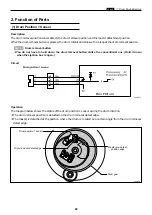
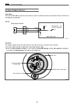
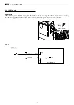
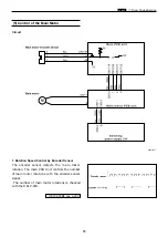
Circuit
Operation
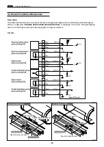
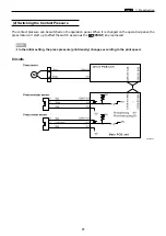
Top and bottom limit of print position is detected by
the vertical registration encoder sensor and the
center sensor.
The center position is detected by the standard
position sensor.
Operation with the Power ON
The printing position returns to the standard
position by operating with the power ON,
depending on the sensor state as follows.
2
When positioned between the standard position
and the bottom limit:
Rotate the vertical registration motor normally (CW)
to return the printing position to the standard.
2
When positioned between the standard position
and the top limit:
Rotate the vertical registration motor reversely (CCW)
to return the printing position to the standard.
R8S02E15e
R8S02G10e
2
The vertical registration encoder sensor
detects the vertical registration motor rotation.
The main PCB unit controls the number of
vertical registration motor rotations with the
vertical registration encoder sensor signal.
NOTE :
Содержание DP-S Series
Страница 1: ......
Страница 9: ......
Страница 11: ......
Страница 16: ...x Dimensions chap 1 15 R8S01001 xDimensions 622 1360 510 228 1080 710 980 688 370 mm...
Страница 22: ...v Part Names and Their Functions chap 1 21 44000A1e 2A 2B 2C R8S01006a 2Detailed drawing...
Страница 33: ...32 z Scanner Section chap 2 Circuit R8S02E03e...
Страница 53: ...52 x Platemaking Master Feed Ejection Section chap 2 2 Master Attach Detach Operation R8S02037e...
Страница 87: ...86 m Drum Section chap 2 2 Circuit R8S02E30...
Страница 171: ...170 MEMO...
Страница 193: ...192 MEMO...
Страница 195: ...194 z Help mode List chap 7 z HELP Mode List...
Страница 243: ...242 c HELP Mode Function and Operation Procedures chap 7...
Страница 270: ...269 c HELP Mode Function and Operation Procedures chap 7...
Страница 281: ...280 MEMO...
Страница 293: ...292 z Electrical Parts Layout and Their Functions chap 9 MEMO...
Страница 294: ...293 x Overall Wiring Layout chap 9 x Overall Wiring Layout Overall Wiring Layout 1 Main PCB 1 2...
Страница 295: ...309 294 x Overall Wiring Layout chap 9 Overall Wiring Layout 1 Main PCB 2 2...
Страница 296: ...310 O 295 x Overall Wiring Layout chap 9 2 Overall Wiring Layout 2 Overall Wiring Layout 2 Drive PCB 1 2...
Страница 297: ...311 296 x Overall Wiring Layout chap 9 Overall Wiring Layout 2 Drive PCB 2 2...
Страница 298: ...297 Reproduction prohibited 1st printing February 2007 Issued by DUPLO SEIKO CORPORATION PRINTED IN JAPAN...

