


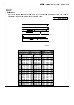


DP-S550
DP-S520 / S510
DP-S850
DP-S620
DP-S650
292.6
0.1mm
Item
39
x
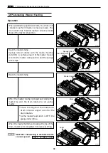
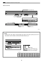
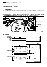
Platemaking / Master Feed / Ejection Section
chap.2
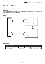
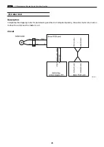
(1)Thermal Head
Description
The thermal elements are in alignment in the primary scanning (vertical direction), and are heated on the
image section to make holes on the master film.
Specifications
Circuit
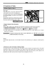
3. Functions of Parts
R8S02E07
No.
1
Picture element density 600DPI (23.6dot/mm)
2
Effective memory width
300DPI (11.81dot/mm) 400DPI (15.7dot/mm)
260.1
0.1mm
300DPI (11.81dot/mm)
260.2
0.2mm
400DPI (15.7dot/mm)
Содержание DP-S Series
Страница 1: ......
Страница 9: ......
Страница 11: ......
Страница 16: ...x Dimensions chap 1 15 R8S01001 xDimensions 622 1360 510 228 1080 710 980 688 370 mm...
Страница 22: ...v Part Names and Their Functions chap 1 21 44000A1e 2A 2B 2C R8S01006a 2Detailed drawing...
Страница 33: ...32 z Scanner Section chap 2 Circuit R8S02E03e...
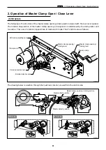
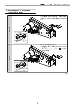
Страница 53: ...52 x Platemaking Master Feed Ejection Section chap 2 2 Master Attach Detach Operation R8S02037e...
Страница 87: ...86 m Drum Section chap 2 2 Circuit R8S02E30...
Страница 171: ...170 MEMO...
Страница 193: ...192 MEMO...
Страница 195: ...194 z Help mode List chap 7 z HELP Mode List...
Страница 243: ...242 c HELP Mode Function and Operation Procedures chap 7...
Страница 270: ...269 c HELP Mode Function and Operation Procedures chap 7...
Страница 281: ...280 MEMO...
Страница 293: ...292 z Electrical Parts Layout and Their Functions chap 9 MEMO...
Страница 294: ...293 x Overall Wiring Layout chap 9 x Overall Wiring Layout Overall Wiring Layout 1 Main PCB 1 2...
Страница 295: ...309 294 x Overall Wiring Layout chap 9 Overall Wiring Layout 1 Main PCB 2 2...
Страница 296: ...310 O 295 x Overall Wiring Layout chap 9 2 Overall Wiring Layout 2 Overall Wiring Layout 2 Drive PCB 1 2...
Страница 297: ...311 296 x Overall Wiring Layout chap 9 Overall Wiring Layout 2 Drive PCB 2 2...
Страница 298: ...297 Reproduction prohibited 1st printing February 2007 Issued by DUPLO SEIKO CORPORATION PRINTED IN JAPAN...