


287
z
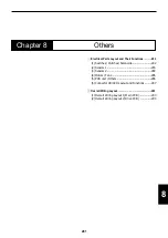
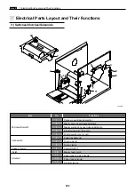
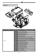
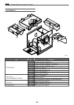
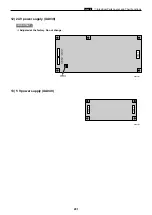
Electrical Parts Layout and Their Functions
chap.9
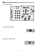
(6) Connector VR/LED Layout and Functions
1) CCD PCB unit : (R8-V325
*
*
)
CCD PCB unit : (R8-V322
*
*
)
CCD PCB unit : (R8-V323
*
*
)
DP-S550/S520/S510
DP-S650/S620
DP-S850
2) Inverter PCB unit (J2-X105
*
*
)
3) LCD Panel (TG014)
R8S09006
¡
Do not remove the CCD PCB or loosen the screw
in the market.
IMPORTANT :
R8S09007
R8S09008
Содержание DP-S Series
Страница 1: ......
Страница 9: ......
Страница 11: ......
Страница 16: ...x Dimensions chap 1 15 R8S01001 xDimensions 622 1360 510 228 1080 710 980 688 370 mm...
Страница 22: ...v Part Names and Their Functions chap 1 21 44000A1e 2A 2B 2C R8S01006a 2Detailed drawing...
Страница 33: ...32 z Scanner Section chap 2 Circuit R8S02E03e...
Страница 53: ...52 x Platemaking Master Feed Ejection Section chap 2 2 Master Attach Detach Operation R8S02037e...
Страница 87: ...86 m Drum Section chap 2 2 Circuit R8S02E30...
Страница 171: ...170 MEMO...
Страница 193: ...192 MEMO...
Страница 195: ...194 z Help mode List chap 7 z HELP Mode List...
Страница 243: ...242 c HELP Mode Function and Operation Procedures chap 7...
Страница 270: ...269 c HELP Mode Function and Operation Procedures chap 7...
Страница 281: ...280 MEMO...
Страница 293: ...292 z Electrical Parts Layout and Their Functions chap 9 MEMO...
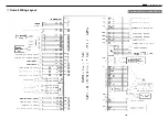
Страница 294: ...293 x Overall Wiring Layout chap 9 x Overall Wiring Layout Overall Wiring Layout 1 Main PCB 1 2...
Страница 295: ...309 294 x Overall Wiring Layout chap 9 Overall Wiring Layout 1 Main PCB 2 2...
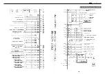
Страница 296: ...310 O 295 x Overall Wiring Layout chap 9 2 Overall Wiring Layout 2 Overall Wiring Layout 2 Drive PCB 1 2...
Страница 297: ...311 296 x Overall Wiring Layout chap 9 Overall Wiring Layout 2 Drive PCB 2 2...
Страница 298: ...297 Reproduction prohibited 1st printing February 2007 Issued by DUPLO SEIKO CORPORATION PRINTED IN JAPAN...