background image

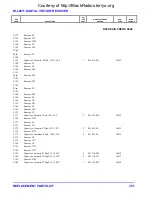
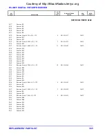
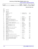
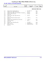
WJ-8611 DIGITAL VHF/UHF RECEIVER 


REF 

DESIG 


DESCRIPTION 

QTY 
PER 

ASSY


MANUFACTURERS 

PART NO. 


MFR. 

CODE 


RECM 

VENDOR 


REPLACEMENT PARTS LIST 

7-71 


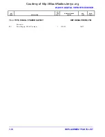
REF DESIG PREFIX A3A2 


R303 

Resistor, Fixed, 390

, ±5%, .1W 

  1   841414-063 

14632 

R304 

Same as R75 

R305 

Same as R37 

R306 

Same as R12 

R307 

Same as R233 

R308 

Same as R15 

R309 

Same as R11 

R310 

Same as R233 

R311 
Thru 

Same as R132 

R313 
R314 

Resistor, Fixed, 68k

, ±5%, .1W 

  2   841414-117 

14632 

R315 

Same as R314 

R316 

Resistor, Fixed, 1.5M

, ±5%, .1W 

  2   841414-149 

14632 

R317 

Same as R316 

R318 

Same as R15 

R319 

Same as R15 

R320 

Same as R123 

R321 

Same as R82 

R322 

Same as R82 

R323 

Same as R233 

R324 

Same as R37 

R325 

Resistor, Variable, Film, 10K

±

10%, .25W 

  1   3262X-1-103 

80294 

R326 

Same as R37 

R327 

Same as R5 

R328 

Same as R9 

R329 

Same as R233 

R330 

Same as R15 

R331 
Thru 

Same as R142 

R335 
R336 

Same as R1 

R337 

Same as R15 

R338 

Resistor, Fixed, 270

, ±5%, .1W 

  1   841414-059 

14632 

R339 

Same as R2 

R340 
Thru 

Same as R37 

R344 
R345 

Same as R5 

R346 

Same as R11 

R347 

Same as R2 

R348 

Same as R12 

R349  
Thru 

Same as R2 

R352  

Courtesy of http://BlackRadios.terryo.org

Содержание WJ-8611

Страница 1: ...HE WJ 8611 DIGITAL VHF UHF RECEIVER P N 181122 001 Revision T Copyright DRS Signal Solutions Inc 1996 All Rights Reserved DRS Technologies DRS Signal Solutions Inc 700 Quince Orchard Road Gaithersburg...

Страница 2: ...WARRANTIES ARE EXCLUSIVE AND IN LIEU OF ALL OTHER WARRANTIES OF MERCHANTABILITY FITNESS FOR PURPOSE OR OTHER WARRANTIES OR GUARANTIES OF ANY KIND OR DESCRIPTION WHETHER STATUTORY EXPRESS OR IMPLIED If...

Страница 3: ...A B blank Courtesy of http BlackRadios terryo org...

Страница 4: ...THIS PAGE INTENTIONALLY LEFT BLANK Courtesy of http BlackRadios terryo org...

Страница 5: ...2 3 Section Two Pages P 2 4 Section Two Page D 2 5 Section Two Page P 2 6 Section Two Page M 2 7 Section Two Page K 2 8 Section Two Page D 2 9 Section Two Page L 2 10 Section Two Page N 2 11 thru 2 1...

Страница 6: ...ection Seven Page S 7 10 Section Seven Page E 7 11 thru 7 12 Section Seven Pages G 7 13 thru 7 14 Section Seven Pages E 7 15 Section Seven Page G 7 16 thru 7 18 Section Seven Pages E 7 19 thru 7 20 Se...

Страница 7: ...blank Foldout G FP 13 FP 14 blank Foldout L FP 15 FP 16 blank Foldout Q FP 17 FP 18 blank Foldout L FP 19 FP 20 blank Foldout L FP 21 FP 22 blank Foldout L FP 23 FP 24 blank Foldout L FP 25 FP 26 bla...

Страница 8: ...WJ 8611 DIGITAL VHF UHF RECEIVER vi LIST OF EFFECTIVE PAGES THIS PAGE INTENTIONALLY LEFT BLANK Courtesy of http BlackRadios terryo org...

Страница 9: ...section cover pages and their back pages Removed intentionally left blank pages and replaced with Notes pages that are formatted with headers and page numbers 9 97 F Incorporated ECO 038860 8 98 G In...

Страница 10: ...WJ 8611 DIGITAL VHF UHF RECEIVER viii REVISION RECORD THIS PAGE INTENTIONALLY LEFT BLANK Courtesy of http BlackRadios terryo org...

Страница 11: ...ions 1 7 1 6 1 8611 SM Signal Monitor Option 1 7 SECTION 2 INSTALLATION Paragraph Page 2 1 Unpacking and Inspection 2 1 2 2 Installation 2 1 2 2 1 Internal Switch Configuration 2 2 2 2 2 Rack Mounting...

Страница 12: ...3 3 Detection Mode Match 3 20 3 3 4 If Bandwidth Selection 3 20 3 3 5 Gain Control Mode Selection 3 21 3 3 6 Squelch Operation 3 22 3 3 7 Noise Blanking Operation 3 23 3 3 8 Beat Frequency Oscillator...

Страница 13: ...Dependent Error Register 4 28 4 6 5 Local Oscillator Error Register 4 29 4 6 6 DSP Error Register 4 30 4 6 7 Hardware Device Error Register 4 31 SECTION 5 CIRCUIT DESCRIPTIONS Paragraph Page 5 1 WJ 8...

Страница 14: ...le Performance Tests 6 12 6 7 1 Type 766032 Switching Power Supply Performance Test 6 13 6 7 2 Type 797228 RF Assembly A3 Performance Test 6 13 6 7 3 Type 797168 Digital Assembly A2 Performance Test 6...

Страница 15: ...nverter PC Assembly A3A2 7 54 7 5 4 Type 766032 1 Power Supply PS1 7 74 APPENDICES Appendix Appendix A 8611 SM Signal Monitor Option LIST OF TABLES Table Page 1 1 Table of Specifications 1 2 1 2 Sensi...

Страница 16: ...ion of Jonathan Type 110QD 20 2 Slide Mounts 2 8 2 4 WJ 8611 Digital VHF UHF Receiver Rear Panel 2 10 2 5 Timing Diagram for I Q Data Transfers at the DIGITAL IF OUT Connector 2 13 2 6 Strobe Output O...

Страница 17: ...ation Drawing 482554 FP 19 FO 11 Type 797168 Digital Control PC Assembly A2 Component Location Drawing 797168 FP 21 FO 12 Part 482902 1st LO 1st Converter PC Assembly A3A1 Component Location Drawing 4...

Страница 18: ...WJ 8611 DIGITAL VHF UHF RECEIVER xvi TABLE OF CONTENTS THIS PAGE INTENTIONALLY LEFT BLANK Courtesy of http BlackRadios terryo org...

Страница 19: ...1 i SECTION 1 GENERAL DESCRIPTION Courtesy of http BlackRadios terryo org...

Страница 20: ...1 ii THIS PAGE INTENTIONALLY LEFT BLANK Courtesy of http BlackRadios terryo org...

Страница 21: ...performed using a DSP algorithm after the signal has been digitized Many of the receiver functions such as fine tuning IF filtering gain control and demodulation are performed digitally using DSP tec...

Страница 22: ...mum LO Phase Noise 95 dBc Hz 10 kHz offset Synthesizer Lock Time 10 msec maximum to within 1 kHz Internal Frequency Accuracy 0 5 x 10 6 5 to 40 C IF Bandwidths 6 dB BW 200 kHz 150 kHz 100 kHz 60 kHz 5...

Страница 23: ...oltage Directive 72 23 EEC EMC Directive 89 336 EEC Table 1 2 Sensitivity Bandwidth kHz Modulation 60 6 dB IFBW Shape Factor Sensitivity dBm 20 to 1000 MHz 0 5 CW 1 0 CW 5 0 AM 10 AM FM 20 AM FM 50 AM...

Страница 24: ...below the parameter display a numeric keypad and a 2 1 2 inch tuning wheel provide the means for front panel control All input and output connectors except for the front panel PHONES jack are located...

Страница 25: ...are includes the following software areas Internal Control Remote Front Panel DSP A DSP B Filters FLEX 1 and FLEX 2 Version 01 00 03 of the Control software was released on February 7 1996 This releas...

Страница 26: ...erent in units with this software version installed from units with earlier versions installed To avoid selection of incorrect bandwidths operators should be aware of the software configuration in the...

Страница 27: ...ON The 8611 SM Signal Monitor Option adds the capability of providing frequency and signal strength information about the 21 4 MHz IF signal to a controlling computer enabling the computer to provide...

Страница 28: ...WJ 8611 DIGITAL VHF UHF RECEIVER 1 8 GENERAL DESCRIPTION NOTES Courtesy of http BlackRadios terryo org...

Страница 29: ...2 i SECTION 2 INSTALLATION Courtesy of http BlackRadios terryo org...

Страница 30: ...2 ii THIS PAGE INTENTIONALLY LEFT BLANK Courtesy of http BlackRadios terryo org...

Страница 31: ...card This card should be used if reshipment of the equipment is required It also contains important warranty adjustment information 4 Carefully inspect the equipment for dents scratches damage or loos...

Страница 32: ...FF position INTERFACE CONTROL MODE Switch A2S1 provides control over the selection of the control mode that the remote interface assumes on receiver power up It also determines if the receiver s IEEE...

Страница 33: ...S1 3 Not Used S1 4 Front Panel Recognition Standard Front Panel Present OFF Default Standard Front Panel Not Present ON S1 5 Not Used S1 6 IEEE 488 Address Update Front Panel Update Enabled OFF Defau...

Страница 34: ...nrf 8611 PRA nrf nrf nrf PRA Loads or reads the preselector configuration data for preselector band A Range nrf 0 255 17 Data Bytes PRB nrf nrf nrf PRB Loads or reads the preselector configuration da...

Страница 35: ...ss 31 positions 1 5 DOWN is not a valid address and should not be used Switch position 8 of A2S2 determines the RS 232 interface baud rate When A2S2 8 is in the Down position the baud rate is fixed at...

Страница 36: ...head screws are used to install each chassis section to a receiver side panel After both chassis sections have been securely tightened to the equipment the cabinet sections are installed into the equ...

Страница 37: ...RACKET CENTERSUPPORTBRACKET HANDLEASSEMBLY OUTSIDEREARHANDLE INSIDEREARHANDLE SPACERSUPPORTBRACKET PARTNO NOM ENCLATURE 9 5 6 8 9 283496 2 283496 1 283496 1 384036 1 282576 2 282576 2 384036 1 10382 A...

Страница 38: ...than Type 110QD 20 2 Slide Mounts A 1 amp slo blo fuse F1 located on the receiver rear panel provides over current protection To replace this fuse turn off the receiver and unplug the line cord from t...

Страница 39: ...ital VHF UHF Receiver Input Output Connectors Connector Reference Designator Description Function Mating Connector Cage Code Comment RF IN J4 50 ohm N Type RF antenna input or other signal source 3031...

Страница 40: ...ivers 21 4 MHz intermediate frequency IF with the RF tuned frequency centered within 1 kHz of 21 4 MHz The bandwidth of the spectrum is 10 MHz typical and the signal level is approximately 14 dB great...

Страница 41: ...nd LO 2nd Converter Subassembly A3A2 This signal will be approximately 34 dB above the level of the RF input signal until the input level reaches 40 dBm At this point the unit s automatic gain control...

Страница 42: ...fferential negative I Q A 4 I or Q Data Indicator 1 I 0 Q I Q B 12 I or Q Data Indicator 0 I 1 Q 5V 14 5V power 12V 7 12V power 12V 15 12V power GND 8 Ground power The data words are 16 bit twos compl...

Страница 43: ...WORD 98 0327 Figure 2 5 Timing Diagram for I Q Data Transfers at the DIGITAL IF OUT Connector Figure 2 6 illustrates two examples of the strobe over a longer period of time several I Q pair transfers...

Страница 44: ...ales representative or the factory Customer Service Department to prevent the possibility of voiding the terms of the warranty Contact the factory via mail telephone wire or cable at DRS Signal Soluti...

Страница 45: ...a firm cushion and to prevent movement inside the container 3 If shipping the unit for service fill out all information on the 5x6 PRODUCT DISCREPANCY REPORT card that was provided with the original s...

Страница 46: ...chard Road Gaithersburg Maryland 20878 1794 U S A When storing the equipment for extended periods follow the above packing instructions to prevent damage to the equipment The safe limits for storage e...

Страница 47: ...3 i SECTION 3 LOCAL OPERATION Courtesy of http BlackRadios terryo org...

Страница 48: ...3 ii THIS PAGE INTENTIONALLY LEFT BLANK Courtesy of http BlackRadios terryo org...

Страница 49: ...ICATORS The receiver front panel contains all of the controls and indicators associated with local operation of the WJ 8611 Digital VHF UHF Receiver Refer to Figure 3 1 as a reference for the controls...

Страница 50: ...z detection mode DET signal strength SIGNAL dBm active gain control mode AGC BFO offset BFO Hz and squelch level SQL dBm as illustrated in Figure 3 2 It also provides displays associated with memory p...

Страница 51: ...el is a 2 1 2 inch diameter knob located in the lower right hand corner of the front panel Its function is to change the receiver s tuned frequency It is functional in the normal and step tuning modes...

Страница 52: ...key is used to select the desired IF bandwidth from the 17 available selections provided by the receiver It is also used in conjunction with the configuration menu paragraph 3 2 9 to customize the sel...

Страница 53: ...on the key illuminates and the currently active gain control mode displayed in the parameter display flashes This indicates that the gain control selection mode is under active control Each press of...

Страница 54: ...ect entry the BFO Offset must be entered with the 1 Hz digit included The last digit entered is a placeholder and does not affect the frequency display The 1 Hz digit is always zero In the shifted mod...

Страница 55: ...QUENCY CONTROL KEY AFC The AFC control key sets the automatic frequency control function on or off This function is selectable in the AM and FM detection modes and only when the active IF bandwidth is...

Страница 56: ...the size of the tuning increments may be set to any value ranging from 000 01 kHz 10 Hz to 100 00 kHz using direct keypad entry or by using the EDIT knob The resolution of the EDIT knob tuning is set...

Страница 57: ...sed the frequency display is updated FREQUENCY TERMINATION KEY MHz The MHz key is used for termination of direct frequency entries As frequency digits are entered they are displayed in the Tuned Frequ...

Страница 58: ...ither of these keys returns the receiver to the normal decade tuning mode The SHIFT LED must be extinguished before the left or right arrow keys are enabled SHIFT KEY SHIFT The SHIFT key places the fr...

Страница 59: ...additional press of the MENU key increments the display to the next menu in the sequence There are nine menus to assist in the configuration as follows 1 IF BANDWIDTH SELECT The IF Bandwidth Select m...

Страница 60: ...he Configuration Menu and returns the receiver to its normal operating mode Pressing the MENU key selects the next item in the Configuration Menu The failure messages associated with BITE are SRAM FAI...

Страница 61: ...the MENU key skips over menu 4 and selects the ADDRESS menu menu 5 If the RS 232 interface is selected pressing the MENU key selects menu 4 4 BAUD RATE The Baud Rate menu is available for selection wh...

Страница 62: ...quency changes per tuning wheel rotation At this selection a complete rotation provides approximately 120 tuning increments SLOW The SLOW rate provides a less responsive tuning wheel response With thi...

Страница 63: ...ides real time control over the time permitting optimum pulse width adjustment while listening to the active signal When in this menu pressing one of the dedicated control keys other than REMOTE exits...

Страница 64: ...uency must be greater than the F1 frequency Otherwise the message OUT OF RANGE is displayed in the display and the entry is not accepted When the F1 and F2 frequencies are entered the Step Size is req...

Страница 65: ...ure is typically 8 dB In the manual operating mode tuning is performed at the front panel by rotation of the tuning wheel by direct entry from the keypad or in the SHIFT mode by using the Left and Rig...

Страница 66: ...sing the left key increments the frequency and pressing the right key decrements the frequency The size of the increments is determined by the flashing digit or by the Step Tune Size NUMERIC ENTRY The...

Страница 67: ...CW The CW selection provides demodulation of continuous wave or interrupted continuous wave type signals In this detection mode all of the available IF bandwidths are available for selection The Auto...

Страница 68: ...last selected IF bandwidth and gain control mode setting In the manual gain mode the detection match feature does not store the actual attenuation setting 3 3 4 IF BANDWIDTH SELECTION There are a tota...

Страница 69: ...excluded from the list 5 When the selection list is completed press the DET key to exit the Configuration menu 3 3 5 GAIN CONTROL MODE SELECTION There are three gain control modes that are available...

Страница 70: ...the receiver activates the audio output and is used in the receiver scan operations to determine if the scan should stop on a signal contact When the SQUELCH key is pressed the LED on the key lights...

Страница 71: ...chevron is extinguished 4 Tune the receiver to the desired signal The above procedure sets the threshold slightly above the ambient noise level Slight additional adjustment may be required depending o...

Страница 72: ...digit to the next digit determining the resolution of the EDIT knob Selection of the BFO frequency may be performed by direct keypad entry in kHz terminated by the BFO key or by rotation of the EDIT...

Страница 73: ...Offset Sets the BFO Offset in the 8000 Hz range when the CW detection mode is programmed CHANNEL PROGRAMMING Programming of the Channel memory is locally performed by tuning the receiver to the desir...

Страница 74: ...lay is updated with the selected status and the display increments to the next channel number The Skip and Include status only affects the activation during a channel scan It does not affect recalling...

Страница 75: ...eter display and the frequency and bandwidth are stored in memory When stored the display increments to the next available lockout channel 4 The lockouts are stored in Lockout memory in the order that...

Страница 76: ...ty greater than the specified squelch threshold level As the scan progresses the frequency display is updated with the frequency at each incremental step of the scan If a signal is detected the receiv...

Страница 77: ...play does not initialize with the one of the scan types displayed continue pressing the SETUP key until the second line of the menu displays one of the three scan types CHANNEL F1 F2 or F1 F2 W LK Rot...

Страница 78: ...m 0 to 600 specify the signal dwell time in seconds 0 to 10 minutes A value of 601 specifies an infinite dwell time It the signal falls below the squelch level before the timer expires the scan resume...

Страница 79: ...00 MHz with a 10 Hz resolution When programming the start and stop frequencies the F1 frequency must be less than the F2 frequency that will be entered in the next step From the numeric keypad enter t...

Страница 80: ...mes to the next increment From the numeric keypad enter the desired Signal Dwell time and terminate the entry by pressing the SETUP key When the entry is terminated the value is momentarily displayed...

Страница 81: ...ickly clearing all receiver memory resetting the front panel parameters to a default setting and resetting internal registers in the receiver circuitry This operation is performed by holding the CE ke...

Страница 82: ...Control Processor to front panel processor communication test failure DUART ERROR RS 232 Interface Write Read test failure FILTER ERROR Digital filter write read test failure LO 1 UNLOCK 1st LO synth...

Страница 83: ...nu is displayed 3 Rotate the EDIT knob to activate BITE At the completion of the BITE tests the word PASSED is displayed to indicate no failures If a failure is detected the error is displayed Pressin...

Страница 84: ...WJ 8611 DIGITAL VHF UHF RECEIVER 3 36 LOCAL OPERATION NOTES Courtesy of http BlackRadios terryo org...

Страница 85: ...4 i SECTION 4 REMOTE CONTROL Courtesy of http BlackRadios terryo org...

Страница 86: ...4 ii THIS PAGE INTENTIONALLY LEFT BLANK Courtesy of http BlackRadios terryo org...

Страница 87: ...e interfaces permits complete control over the receiver operations The information in this section provides all of the commands and formatting information necessary to control and monitor the receiver...

Страница 88: ...e the end of a transfer sequence EOI The fifth management line REN is not used in this configuration The IEEE 488 interface provides the receiver with talk and listen capabilities when commanded by th...

Страница 89: ...FORMATS Query responses from the receiver are transmitted in a fixed field format The response begins with the three character mnemonic of the query in upper case characters followed by a numeric argu...

Страница 90: ...han one half nr1 The nr1 is a numeric response format for integers composed of an optional sign field followed by any number of digits The decimal point is implicitly defined to always follow the last...

Страница 91: ...frequency BWA BWA nr1 Requests the currently active IF bandwidth Range 1 17 See BWS command Reset BWA 8 Default BWA 8 BWC nrf Selects an IF bandwidth by specifying its size in MHz If the specified si...

Страница 92: ...BYP 0 Bypass off BYP 1 Bypass on BYP BYP nr1 Requests the current bypass path status Reset BYP 0 Default BYP 0 CFG CFG nr1 Requests the status of the receiver s configuration mode The data returned c...

Страница 93: ...re COO 0 Override Off COO 1 Override On COO COO nr1 Request the current setting of the COR Output Override mode Reset 0 Default 0 COR nrf Sets the threshold above which the receiver recognizes a signa...

Страница 94: ...IF bandwidth The value returned is the percentage of the active IF bandwidth in the range of from 50 to 50 A positive value indicates that the signal frequency is greater than the receiver s tuned fre...

Страница 95: ...nd into the selected channel The channel number assigned with this command remains constant as channels are added or deleted The data assigned with the LCK command overwrites any previously stored dat...

Страница 96: ...timer setting Reset PDW 000 Default PDW 000 PRE nrf Sets the preselector tuning voltage for the current tuned frequency It is used for test purposes only Range 0 255 Where 0 255 tuning voltages from 0...

Страница 97: ...Default All lockout channels contain 0000 0000 RMD nrf SMD nr1 nr1 nr2 nr1 nr 1 nr1 nr1 nr1 nr1 nr 1 nr1 nr1 nr2 nr2 nr2 nr1 nr2 nr2 Recalls the parameters from the specified memory channel Refer to...

Страница 98: ...ers Each data item in the list is separated by a comma Any blank data field causes the associated parameter to remain unchanged The data may be terminated after any completed field causing any fields...

Страница 99: ...ly programmed channel scan list Reset STL 001 200 Default STL 001 200 Example STL 001 002 020 101 STO nrf Stores the current receiver parameters into the selected receiver memory channel Range 1 200 S...

Страница 100: ...ault AGC 1 ATN nrf Sets the receivers signal attenuation This command controls the gain of the receiver when in the manual gain control mode It permits from 0 to 100 dB of attenuation to be selected i...

Страница 101: ...ummary Enable 3 8 DPR DSP Error Bit Summary Enable 4 16 DVR Hardware Device Error Bit Summary Enable 5 7 Not Used DEE DEE nr1 Requests the status of the Device Dependent Error Enable register The resp...

Страница 102: ...Not Used 7 128 ACM DSP A to Control Processor Communication Error DPE DPE nr1 Requests the status of the DSP Error Enable register The response data is a decimal number containing the sum of the bit...

Страница 103: ...Read Error Enabled 6 64 IFE IF Filter Write Read Error Enabled 7 128 TMT BIT Timeout Error Enabled DVE DVE nr1 Requests the status of the Hardware Device Error Enable register The response data is a d...

Страница 104: ...nr1 Requests the status of the Event Summary Enable register The response data is a decimal number containing the sum of the bit values of the Event Summary Enable register as defined in the ESE comma...

Страница 105: ...OR Error Enable register as defined in the LOE command description LOR LOR nr1 Requests the status of the LO Error register The response is a decimal number containing the sum of the bit values of the...

Страница 106: ...Requests the status of the Receiver Status Enable register The response data is a decimal number containing the sum of the bit values of the Receiver Status Enable register as defined in the RSE comm...

Страница 107: ...er Status Bit Enable 1 Not Used 2 Not Used 3 Not Used 4 16 MAV Message Available 5 32 ESB Event Summary Bit Enable 6 64 RQS Request Service Bit Enable 7 Not Used SRE SRE nr1 Requests the status of the...

Страница 108: ...48 DUART Write Read Error 12 4096 IF Filter Write Read Error 13 8192 Video Filter Write Read Error 14 Not Used 15 Not Used 16 Not Used 17 Not Used 18 262144 13 5 Vdc Power Supply Error 19 524288 24 Vd...

Страница 109: ...Example CDT 09 25 95 COP nrf Enter options installed in unit Currently not used COP COP nr1 Requests options installed in unit Currently not used CSN nrf Writes the receiver serial number Range 0 9999...

Страница 110: ...nr1 nr1 nr1 Requests the preselector configuration data list for band D The response includes the 18 factory programmed data bytes that define the tuning response of preselector band D PRE nrf nrf nr...

Страница 111: ...ish which event has caused the receiver to assert the SRQ The STB query response includes similar information as detailed below SRQ For RS 232 operations the SRQ is a one byte control character ESC in...

Страница 112: ...ng paragraphs detail the function and use of the Event Summary Register and the ESR query Table 4 5 provides the bit evaluation of this register and defines the bit functions The Event Summary Registe...

Страница 113: ...or when a valid message can not be executed due to a device error condition 05 CME Command Error This bit is set when an unrecognized message header is received 06 Not Used 07 PON Power On This bit is...

Страница 114: ...Scan and the scan is suspended on the signal 05 07 Not Used 4 6 4 DEVICE DEPENDENT ERROR REGISTER The Device Dependent Error Register determines what error conditions have caused the DDE bit of the E...

Страница 115: ...he LOS bit of the Device Dependent Error Register to be set The LOE command sets the enable bits to select which conditions are enabled The LOR query reads the contents of the error register to identi...

Страница 116: ...cation error between DSP B and DSP A It occurs when DSP A does not respond to DSP B 02 GCP Gain Control Error This bit is set on a communication error between DSP B and the Gain Control Processor It o...

Страница 117: ...BITE when the checksum test for the Control Processor s EPROMs fails 01 E2 P EEPROM Error Occurs on power up or at the completion of BITE when the Control Processor s EEPROM fails a write read test 02...

Страница 118: ...ed Bit Mnemonic Description 06 IFE IF Filter Error Occurs on power up or at the completion of BITE when the Digital Filters used for IF Filtering fail a write read test 07 TMT BITE Timeout Occurs on p...

Страница 119: ...5 i SECTION 5 CIRCUIT DESCRIPTIONS Courtesy of http BlackRadios terryo org...

Страница 120: ...5 ii THIS PAGE INTENTIONALLY LEFT BLANK Courtesy of http BlackRadios terryo org...

Страница 121: ...rcuitry for further processing A second IF output that is centered at 21 4 MHz is sent to the rear panel The 21 4 MHz IF output is a wide band output for use with an external signal monitor or spectra...

Страница 122: ...and video signal intelligence is converted back to analog signals and are routed to the audio and video outputs At the rear panel terminal bus TB1 provides the audio at LINE A and LINE B With AM FM C...

Страница 123: ...18 as a reference for the RF Tuner Assembly A3 functional description The RF input enters the RF Tuner Assembly A3 at connector J1 of the 1st LO 1st Converter PC Assembly A3A1 This input spectrum ran...

Страница 124: ...nuator bypassed The Input protection circuit provides protection for the pin diode switching circuits at the input to the tracking preselector It enables the receiver to withstand continuous input lev...

Страница 125: ...om the preselector the RF spectrum is amplified and filtered prior to conversion The lowpass filter is an elliptical filter that provides a flat response from 0 to 1000 MHz and rapidly rolls off above...

Страница 126: ...d using the following formula FREQLO1 INT RF 18 351 2 5 x 2 5 1370 or INT RF 1 649 2 5 x 2 5 1350 Where FREQLO1 is the 1st LO frequency in MHz RF is the Tuned Frequency in MHz The oscillator consists...

Страница 127: ...depending on where in the active VCO band the oscillator is tuned If the synthesizer fails to lock on frequency this voltage will swing to its minimum or maximum extreme 0 V or 22V The operating power...

Страница 128: ...zer is tuned to 1327 75 MHz and this signal is down converted to 21 4 MHz 1349 150 MHz 1327 750 MHz 21 4 MHz The IF spectrum is bandpass filtered and then split into two signal paths The first signal...

Страница 129: ...of the allowable frequencies 1 2 5 10 MHz and monitors the REF LOCK line A3A2P3 pin 29 for a locked condition logic 1 If no lock is obtained or if the external reference signal is removed the Digital...

Страница 130: ...to the control circuitry Under normal operating conditions the phase detector provides a tuning voltage of approximately 6 V to the VCO for frequency control Capacitor C204 in the tuned circuit is adj...

Страница 131: ...onship between the Step Loop Resolution Loop and the 2nd LO Output frequencies The frequencies of the Step Loop and Resolution Loop are determined by the following formulas FREQSTEP INT FREQLO2 1327 7...

Страница 132: ...ble A3A2P3 RFB DATA Its serial transfer is synchronized with the data clock at A3A2P3 pin 19 RFB CLK During the data transfer the data and clock signals are directed to all of the circuits in the RF T...

Страница 133: ...le attenuation ranging from 0 to approximately 31 dB that may be injected into the signal path between the 1350 MHz IF Input A2E5 and the 250 kHz IF Output A2P1 of the 2nd LO 2nd Converter PC Assembly...

Страница 134: ...g configuration of the receiver Switch S2 selects the default configuration of the receiver s remote interface It selects the type interface that will be active IEEE 488 or RS 232 and determines the r...

Страница 135: ...be line forces the intended data register in the RF Tuner Assembly A3 to accept the data The data is directed to the appropriate data register by the RFB A0 A1 A2 parallel control lines Each time data...

Страница 136: ...detect and sense lines the Control Processor Section also monitors the level of the 250 kHz IF input signal after it is digitized It attempts to prevent the IF signal from exceeding the input limits...

Страница 137: ...ly Controlled Oscillator and two 32 bit DSP Processors DSP A and DSP B These processing components interface with the Control Processor section and other support circuits through two programmable Flex...

Страница 138: ...kHz 6 4 kHz 5 0 kHz 3 2 kHz 31 25 kHz 62 5 kHz 1 0 kHz 5 kHz 2 kHz 3 90265 kHz 7 8053 kHz If ISB detection mode is selected the I and Q data transfer rate is 15 125 kHz and the strobe rate is 30 25 kH...

Страница 139: ...obtain a 4 2 MHz 4 167 MHz clock for use by the IEEE 488 remote interface 5 4 TYPE 797229 1 FRONT PANEL ASSEMBLY A1 CIRCUIT DESCRIPTION The Front Panel Assembly A1 consists of the Part 482554 2 Front...

Страница 140: ...nals are used by the four Dot Matrix ICs to display the appropriate parameters The Front Panel Assembly A1 features a switch matrix consisting of a 16 key keyboard and 16 individual pushbuttons Each k...

Страница 141: ...iding reliable outputs to the receiver over a wide range of input voltages and line frequencies It operates from 97 to 253 Vac at line frequencies ranging from 47 to 440 Hz The input circuitry of this...

Страница 142: ...WJ 8611 DIGITAL VHF UHF RECEIVER 5 22 CIRCUIT DESCRIPTIONS NOTES Courtesy of http BlackRadios terryo org...

Страница 143: ...6 i SECTION 6 MAINTENANCE Courtesy of http BlackRadios terryo org...

Страница 144: ...6 ii THIS PAGE INTENTIONALLY LEFT BLANK Courtesy of http BlackRadios terryo org...

Страница 145: ...s for looseness wear and other signs of deterioration The circuit card assemblies should be checked to assure that they are properly secured to the chassis and making good electrical contact Electroni...

Страница 146: ...6 600 Ohm Stereo with 1 4 inch Tip Ring Jack Frequency Standard HP 5061A Cesium Beam Standard 10 MHz 6 6 WJ 8611 DIGITAL VHF UHF RECEIVER PERFORMANCE TESTS The receiver performance tests that follow...

Страница 147: ...ATOR PERFORMANCE 1 Apply power to the receiver and observe the power up sequence Verify that all of the front panel LED displays and indicators light with uniform brilliance during the power up LED te...

Страница 148: ...uency 10 0000 MHz Output Level 5 dBm Modulation Off 5 Connect the signal generator to the receiver s External Reference connector EXT REF Press the front panel MENU key as required to display the Refe...

Страница 149: ...ver Connect the RF millivoltmeter and 50 ohm load to the SDU Output as illustrated in Figure 6 2 95 1208 RF MILLIVOLT METER WJ 8611 VHF UHF RECEIVER SIGNAL GENERATOR RF INPUT PHONES 600 OHM HEADSET 50...

Страница 150: ...as follows Tuned Frequency 250 00000 MHz IF BW 20 0 kHz Detection AM Gain Control AGC Fast Squelch Off 4 Verify the SIGNAL dBm display on the front panel indicates between 80 and 110 dBm 5 While obse...

Страница 151: ...ing the SQUELCH Key set the Squelch function to ON Verify that no audio is present at the headphones Verify that approximately 5 Vdc is present at the COR output as measured by the digital voltmeter 6...

Страница 152: ...output to 40 dBm With the squelch level exceeded the voltmeter should read near 0 V Set the signal generator output to a level of 80 dBm With the signal below the squelch level the voltmeter should r...

Страница 153: ...least 10 dB 7 Repeat steps 5 and 6 using each of the IF bandwidths and associated signal generator output levels listed in Table 6 2 8 Set the receiver as follows Tuned Frequency 250 00000 MHz Detecti...

Страница 154: ...3 dBm 400 Hz 3 0 kHz 20 kHz 100 dBm 400 Hz 6 0 kHz 100 kHz 93 dBm 400 Hz 30 0 kHz 200 kHz 90 dBm 400 Hz 60 0 kHz 6 6 8 AUDIO OUTPUT DISTORTION PERFORMANCE TEST 1 Connect the test equipment as illustra...

Страница 155: ...stortion analyzer function control to the Distortion position Slowly adjust the distortion analyzer frequency control for a minimum indication on the meter Reset the meter range as required for the be...

Страница 156: ...increase in the RF input signal level 6 7 WJ 8611 MODULE PERFORMANCE TESTS The module test procedures in this section assist in isolating a fault to a malfunctioning module or subassembly These proce...

Страница 157: ...fy that the voltage at this connector reflects the current AC line voltage at the power source 6 7 2 TYPE 797228 RF TUNER ASSEMBLY A3 PERFORMANCE TEST 1 Refer to Foldouts FO 8 and FO 13 From the top o...

Страница 158: ...peak to peak or less 11 Reconnect A3A2P1 to the J2 connector 12 From the underside of the receiver remove the A3A2P2 connector from J4 on the Digital Assembly A2 Using the oscilloscope check the sign...

Страница 159: ...iver check the red RUN LED DS1 on the Digital Assembly Verify that the LED is flashing indicating that the control processor is operational 3 Verify that the proper 100 MHz reference from the RF assem...

Страница 160: ...g the signal level slowly tune the signal generator down in frequency to 19 9970 MHz Verify that the signal level remains constant throughout the frequency range 14 Remove the oscilloscope from the Li...

Страница 161: ...test procedure to verify its operation 6 Connect the oscilloscope at pin 2 RXD of J29 A constant level of approximately 7 Vdc should be present until one of the front panel controls is operated Opera...

Страница 162: ...six screws that secure the RF Assembly to the receiver s mounting deck Refer to Figure 6 7 for screw location 6 At the receiver rear panel remove the hex nuts and washers from the EXT REF and SDU conn...

Страница 163: ...WJ 8611 DIGITAL VHF UHF RECEIVER MAINTENANCE 6 19 00 0084 Figure 6 7 Type 797228 1 RF Tuner Assembly A3 Screw Location Courtesy of http BlackRadios terryo org...

Страница 164: ...W1P1 RS232 Cable J12 W3P1 IEEE 488 Cable J14 W4P1 DIGITAL IF OUT J29 W5P2 To Front Panel A2E1 W6P1 Power Supply Input WARNING If scrapping this assembly remove lithium battery BT1 and dispose of it i...

Страница 165: ...in reverse order of the removal 6 8 4 PART 482554 FRONT PANEL CONTROL PC ASSEMBLY A1A1 REMOVAL AND REPLACEMENT 1 Remove front panel as described in the Type 797229 Front Panel Assembly A1 Removal and...

Страница 166: ...tom covers to gain access to the internal assemblies 3 From the underside of the chassis unplug W6P1 from A2E1 of the Digital Control PC Assembly A2 Remove cable from cable restraint 4 From the unders...

Страница 167: ...7 i SECTION 7 REPLACEMENT PARTS LIST Courtesy of http BlackRadios terryo org...

Страница 168: ...7 ii THIS PAGE INTENTIONALLY LEFT BLANK Courtesy of http BlackRadios terryo org...

Страница 169: ...drawings and illustrations in the figure titles in parenthesis 7 2 1 PROVISIONING NOTE INCONSISTENCIES IN PART NUMBERING CONVENTIONS The internal computer applications at the factory have undergone u...

Страница 170: ...Shore Rd No 600 Palo Alto CA 94303 04713 Motorola Inc Semiconductor Products Sector 5005 E McDowell Rd Phoenix AZ 85008 4229 0TZP6 Sumida Electric Co 637 E Golf Rd Suite 209 Arlington Heights IL 6000...

Страница 171: ...ylvan Road P O Box 1044 Woburn MA 01801 1854 12855 Trak Microwave Co 4726 Eisenhower Blvd Tampa FL 33634 6391 17856 Siliconix Inc 2201 Laurelwood Rd Santa Clara CA 95054 1516 14482 Watkins Johnson Co...

Страница 172: ...eld Rd Mountain View CA 94043 4008 27014 National Semiconductor Corp 2900 Semiconductor Drive Santa Clara CA 95051 0606 34335 Advanced Micro Devices Inc 901 Thompson Pl PO Box 3453 Sunnyvale CA 94086...

Страница 173: ...737 56289 Sprague Electric Co World Hqs 267 Lowell Rd Hudson NH 03051 4900 51406 Murata Erie North America Inc Headquarters and Georgia Opns 2200 Lake Park Dr Smyrna GA 30080 58982 Precision Connector...

Страница 174: ...Inc 1200 Columbia Ave Bldg C Riverside CA 92507 64155 Linear Technology Corp 1630 Mccarthy Blvd Milpitas CA 95035 7487 8J671 Crane Component Co 4000 Crane Centre Dr Streetsboro OH 44240 5076 67183 Alt...

Страница 175: ...a guide to aid the user of the equipment while in the field The parts listed may not necessarily be identical with the parts installed in the unit The parts listed in paragraph 7 5 will provide for s...

Страница 176: ...or Plug SMA For RD 316 1 9001 9023 019 19505 W3 Cable Assembly 1 383522 2 14632 W3P1 Connector Plug 24 Socket 1 66900 124 22526 W4 Cable Assembly 1 383931 1 14632 W4P1 Connector Plug 16 position Femal...

Страница 177: ...MP5 Switch Cap 12mm Marked 5 1 383072 5 14632 MP6 Switch Cap 12mm Marked 6 1 382072 6 14632 MP7 Switch Cap 12mm Marked 1 1 383072 1 14632 MP8 Switch Cap 12mm Marked 2 1 382072 2 14632 MP9 Switch Cap 1...

Страница 178: ...4 VJ1812Y104KXBMT 95275 C8 Same as C7 C9 Same as C7 C10 Same as C1 C11 Same as C1 C12 Capacitor Tantalum 47 F 20 16V 3 841293 30 14632 C13 Same as C12 C14 Same as C1 C15 Capacitor Tantalum 4 7 F 20 2...

Страница 179: ...Not Used C66 Not Used C67 Same as C1 C68 Same as C1 C69 Thru Same as C39 C79 C80 Capacitor Ceramic 100pF 2 50V 4 841416 049 14632 C81 Thru Same as C80 C83 C84 Not Used C85 Not Used C86 Thru Same as C...

Страница 180: ...d J11 Not Used L1 Inductor Choke 1 H 3 NLC565050T 1R0K 54583 L2 Same as L1 L3 Same as L1 L4 Inductor 4 7 H 10 Q 7 1 NLC565050T 4R7K 7J069 Q1 Transistor PNP 16 MMBT2907ALT1 04713 Q2 Thru Same as Q1 Q16...

Страница 181: ...xed 2 2k 5 1W 16 841414 081 14632 R68 Resistor Fixed 22 0 5 125 W 16 841296 025 14632 R69 Same as R67 R70 Same as R68 R71 Same as R67 R72 Same as R68 R73 Same as R67 R74 Same as R68 R75 Same as R67 R7...

Страница 182: ...1 R102 R103 Thru Same as R15 R106 R107 Thru Same as R1 R110 R111 Same as R99 R112 Same as R99 R113 Thru Same as R1 R116 R117 Resistor Fixed 100 5 1W 5 841414 049 14632 R118 Thru Same as R117 R121 R122...

Страница 183: ...as U7 U9 Integrated Circuit SRAM 32K X 8 MT5C2568DJ 20 6Y440 U10 Integrated Circuit EPROM 64KX16 1 TMS27PC210A 12FNL 01295 XU10 Socket Leadless Chip Carrier 1 213 044 601 26742 U11 Not Used XU11 Not U...

Страница 184: ...een Diffused 1 HLMP 1503 28480 DS11 LED Yellow Rectangular 2 HLMP S300 28480 DS12 Same as DS11 J1 Connector 44 position 1 PGM44DS G40T30 8J671 P1 Connector 16 Pin Terminal Strip 1 HTSW 108 07 G D 5532...

Страница 185: ...ru Same as S2 S24 S25 Same as S1 S26 Thru Same as S2 S28 S29 Same as S1 S30 Same as S1 S31 Same as S2 S32 Same as S2 U1 Display 7 Segment Green 9 HDSP 7803 28480 U2 Thru Same as U1 U4 U5 Not Used U6 T...

Страница 186: ...MFR CODE RECM VENDOR 7 18 REPLACEMENT PARTS LIST 7 5 1 3 TYPE 383947 1 INTERCONNECT PC ASSEMBLY REF DESIG PREFIX A1A3 Revision A P1 Connector Header 1 M80 8871805 KQ536 R1 Encoder Modification 1 28349...

Страница 187: ...C13 C34 Same as C13 C35 Thru Same as C1 C40 C41 Capacitor Ceramic 100pF 5 50V 33 841415 007 14632 C42 Thru Same as C1 C44 C45 Capacitor Ceramic 20pF 2 50V 2 841416 032 14632 C46 Capacitor Ceramic 82p...

Страница 188: ...4 C87 Not Used C88 Thru Same as C1 C90 C91 Capacitor Tantalum 4 7 F 20 16V 2 T491A475K016AS 31433 C92 Same as C1 C93 Same as C91 C94 Same as C1 C95 Same as C13 C96 Thru Same as C1 C120 C121 Same as C1...

Страница 189: ...151 Same as C1 C152 Same as C131 C153 Capacitor Ceramic 033 F 10 50V 10 841415 022 14632 C154 Capacitor Ceramic 100pF 2 50V 1 841416 049 14632 C155 Capacitor Ceramic 1200pF 2 50V 2 841416 075 14632 C1...

Страница 190: ...C214 Same as C158 C215 Thru Same as C1 C220 C221 Same as C131 C222 Same as C131 C223 Same as C1 C224 Same as C41 C225 Same as C41 C226 Same as C1 C227 Same as C41 C228 Same as C41 C229 Thru Same as C...

Страница 191: ...C260 Same as C155 C261 Thru Same as C1 C282 C283 Thru Same as C13 C285 C286 Same as C1 C287 Same as C13 C288 Thru Same as C1 C296 C297 Same as C45 C298 Same as C1 C299 Same as C1 C300 Same as C13 C301...

Страница 192: ...as C1 C334 Thru Same as C41 C340 C341 Same as C1 C342 Same as C312 C343 Thru Same as C41 C354 C355 Thru Same as C153 C360 C361 Thru Same as C1 C363 C364 Same as C124 C365 Same as C124 C366 Same as C1...

Страница 193: ...e as J2 J10 Same as J7 J11 Same as J7 J12 Same as J5 J13 Same as J7 J14 Connector 16 Pin Terminal Strip 2 HTSW 108 07 G D 55322 J15 Connector Header 8 Pin Header 1 TSW 104 07 G D 55322 J16 Same as J1...

Страница 194: ...xed 3 3k 5 1W 12 841414 085 14632 R2 Same as R1 R3 Resistor Fixed 10k 5 1W 231 841414 097 14632 R4 Resistor Fixed 10 5 1W 26 841414 025 14632 R5 Thru Same as R4 R9 R10 Resistor Fixed 100 5 1W 31 84141...

Страница 195: ...Same as R3 R61 Not Used R62 Same as R22 R63 Thru Same as R3 R73 R74 Same as R34 R75 Not Used R76 Resistor Fixed 470 5 1W 3 841414 065 14632 R77 Not Used R78 Same as R3 R79 Resistor Fixed 680k 5 1W 3...

Страница 196: ...6 Same as R76 R107 Same as R4 R108 Same as R4 R109 Same as R103 R110 Same as R4 R111 Same as R4 R112 Not Used R113 Thru Same as R3 R115 R116 Not Used R117 Same as R3 R118 Same as R4 R119 Not Used R120...

Страница 197: ...2 841414 129 14632 R156 Same as R155 R157 Resistor Fixed 68 5 1W 2 841414 045 14632 R158 Same as R157 R159 Resistor Fixed 1 5k 5 1W 4 841414 077 14632 R160 Thru Same as R159 R162 R163 Same as R10 R164...

Страница 198: ...23 Same as R18 R224 Same as R90 R225 Resistor Fixed 1 1k 5 1W 1 841414 074 14632 R226 Same as R103 R227 Thru Same as R4 R229 R230 Same as R18 R231 Same as R3 R232 Resistor Fixed 12k 5 1W 1 841414 099...

Страница 199: ...Same as R10 R276 R277 Thru Same as R3 R281 R282 Thru Same as R10 R285 R286 Thru Same as R3 R290 R291 Thru Same as R34 R302 R303 Not Used R304 Same as R34 R305 Same as R3 R306 Same as R3 R307 Same as R...

Страница 200: ...r Fixed 5 6k 5 1W 4 841414 091 14632 R422 Thru Same as R421 R424 R425 Same as R254 R426 Same as R93 R427 Thru Same as R3 R443 R444 Same as R18 R445 Same as R18 R446 Same as R27 R447 Varistor 100k 20 2...

Страница 201: ...ircuit Fast Dual JK Pos Edge Trig Flip Flop 1 74F109 SO16 04713 U6 Integrated Circuit Quad 2 Input AND Gate 1 74F08 SO14 18324 U7 Integrated Circuit SRAM 128K X 8 4 MT5C1008DJ 25 6Y440 U8 Thru Same as...

Страница 202: ...r 1 MC68331CFC16 04713 U54 Integrated Circuit SRAM 128K X 8 2 MT5C1008DJ 25PLT 6Y440 U55 Same as U54 U56 Integrated Circuit EPROM 2MB Programmed 1 842129 001 14632 XU56 Socket Leadless Chip Carrier 2...

Страница 203: ...uit SRAM Non Volatile Controller 1 BQ2203ASN TBD03 U85 Same as U81 U86 Same as U43 U87 Same as U59 U88 Not Used U89 Same as U81 U90 Same as U81 U91 Integrated Circuit Line Driver 1 MC3453D 01295 U92 I...

Страница 204: ...RF TUNER ASSEMBLY REF DESIG PREFIX A3 Revision E1 A1 1st LO 1st Converter PC Assembly 1 482902 1 14632 A2 2nd LO 2nd Converter PC Assembly 1 482903 1 14632 MP1 Rod 2 283608 1 14632 MP2 Same as MP1 RFT...

Страница 205: ...004 14632 C33 Same as C1 C34 Same as C30 C35 Same as C1 C36 Capacitor Tantalum 4 7 F 20 20V 3 841293 25 14632 C37 Capacitor Ceramic 100pF 5 50V 32 841415 007 14632 C38 Capacitor Ceramic 3 0pF 1 pF 500...

Страница 206: ...47 F 10 25V 7 VJ1210Y474KXXMT 95275 C90 Same as C36 C91 Same as C89 C92 Same as C1 C93 Thru Same as C37 C97 C98 Same as C88 C99 Same as C36 C100 Same as C1 C101 Capacitor Tantalum 100 F 20 10V 10 T49...

Страница 207: ...5 50V 1 841415 010 14632 C138 Thru Same as C1 C140 C141 Same as C37 C142 Same as C37 C143 Capacitor Tantalum 33 F 20 16V 3 841293 22 14632 C144 Same as C1 C145 Thru Same as C30 C147 C148 Capacitor Cer...

Страница 208: ...ame as C30 C187 Same as C1 C188 Same as C1 C189 Same as C65 C190 Thru Same as C1 C197 C198 Same as C30 C199 Same as C30 C200 Capacitor Ceramic 7pF 05pF 150V 1 ATC100A0R7AW150X 29990 C201 Same as C1 C2...

Страница 209: ...ame as C65 C244 C245 Thru Same as C1 C248 C249 Same as C65 C250 Same as C65 C251 Thru Same as C1 C253 C254 Same as C65 C255 Same as C101 C256 Same as C101 C257 Same as C1 C258 Same as C101 C259 Same a...

Страница 210: ...Same as C37 C281 Same as C37 C282 Same as C1 C283 Same as C101 C284 Same as C1 CR1 Diode PIN 20 HSMP 3892 T31 28480 CR2 Diode Varactor 22 MA4ST409CK 96341 CR3 Thru Same as CR2 CR6 CR7 Diode Varactor...

Страница 211: ...CR50 CR71 Same as CR50 DS1 LED Red Subminiature 1 HLMP 6620 031 28480 FB1 Not Used FB2 Not Used FB3 Ferrite Bead 1 CB70 201209T 54583 FL1 1350 MHz Bandpass Filter Assembly 1 383840 1 14632 XFL1 2 Sock...

Страница 212: ...41 Inductor Spring 12 5nH 5 5 A04T 02113 L42 Thru Same as L41 L45 L46 Same as L40 L47 Inductor Spring 2 5nH 10 2 A01T 02113 L48 Inductor 100nH 5 2 841438 025 14632 L49 Same as L1 L50 Inductor 1 0 H 20...

Страница 213: ...L90 Same as L50 L91 Same as L50 L92 Inductor Spring 5 0nH 10 2 A02T 02113 L93 Same as L92 L94 Same as L62 L95 Same as L62 L96 Same as L48 Q1 Transistor FET 0 5 6 GHz 2 ATF 21186 28480 Q2 Not Used Q3...

Страница 214: ...4 Q36 Same as Q4 R1 Resistor Fixed 680 5 1W 21 841414 069 14632 R2 Resistor Fixed 27k 5 1W 22 841414 107 14632 R3 Same as R2 R4 Resistor Fixed 1 0k 5 1W 35 841414 073 14632 R5 Same as R2 R6 Same as R4...

Страница 215: ...2 R49 Resistor Fixed 47 5 1W 5 841414 053 14632 R50 Same as R48 R51 Resistor Fixed 390 5 1W 1 841414 063 14632 R52 Not Used R53 Same as R46 R54 Resistor Fixed 1 5 5 1W 1 841414 005 14632 R55 Resistor...

Страница 216: ...414 065 14632 R91 Same as R90 R92 Same as R90 R93 Thru Same as R46 R96 R97 Same as R4 R98 Same as R46 R99 Same as R42 R100 Same as R46 R101 Same as R4 R102 Resistor Fixed 33k 5 1W 1 841414 109 14632 R...

Страница 217: ...or Fixed 100k 5 1W 2 841414 121 14632 R136 Same as R129 R137 Same as R59 R138 Same as R42 R139 Same as R135 R140 Same as R42 R141 Same as R42 R142 Resistor Fixed 91k 5 1W 55 125C 7 841414 120 14632 R1...

Страница 218: ...R193 Same as R185 R194 Same as R185 R195 Same as R46 R196 Same as R180 R197 Same as R1 R198 Same as R120 R199 Same as R184 R200 Same as R185 R201 Same as R185 R202 Same as R13 R203 Same as R13 R204 S...

Страница 219: ...d 3 3k 5 1W 2 841414 085 14632 R235 Not Used R236 Same as R46 R237 Same as R180 R238 Same as R1 R239 Thru Not Used R245 R246 Thru Same as R1 R248 R249 Same as R46 R250 Thru Same as R42 R255 R256 Thru...

Страница 220: ...RF 1 QBH 147 55027 U2 Mixer 1 WJ SM4TH 14482 U3 Amplifier 1 VNA 25 15542 U4 Amplifier GAAS 2 CGY 50 0CF99 U5 Same as U4 U6 Amplifier CMOS Dual Operational 1 LMC662CM 27014 U7 Integrated Circuit 8 Sta...

Страница 221: ...ter 500 2000 MHz 1 SPL 2EF 01 12855 U25 Integrated Circuit Voltage Regulator 5V 4 TK11550MT TOKO U26 Integrated Circuit Wide Band Amplifier 1 UPC2711T 4T165 U27 Integrated Circuit Divide By 2 Prescale...

Страница 222: ...c 100pF 2 50V 3 841416 049 14632 C5 Capacitor Ceramic 33pF 2 50V 5 841416 037 14632 C6 Capacitor Ceramic 470pF 2 50V 3 841416 065 14632 C7 Capacitor Ceramic 56pF 2 50V 2 841416 043 14632 C8 Capacitor...

Страница 223: ...61 Capacitor Ceramic 6800pF 10 50V 1 841415 018 14632 C62 Same as C9 C63 Capacitor Ceramic 2200pF 10 50V 1 841415 015 14632 C64 Same as C38 C65 Same as C38 C66 Same as C38 C67 Capacitor Variable 2 6pF...

Страница 224: ...r Ceramic 3 3pF 1pF 50V 1 841416 013 14632 C106 Same as C9 C107 Same as C9 C108 Same as C59 C109 Same as C45 C110 Thru Same as C9 C112 C113 Capacitor Ceramic 3 6pF 1pF 50V 2 841416 014 14632 C114 Same...

Страница 225: ...Same as C45 C165 Same as C9 C166 Same as C9 C167 Same as C45 C168 Same as C9 C169 Same as C45 C170 Same as C9 C171 Capacitor Ceramic 15pF 2 50V 2 841416 029 14632 C172 Same as C171 C173 Same as C9 C1...

Страница 226: ...Same as C183 C202 C203 Same as C5 C204 Capacitor Variable 4 5 20pF 50V 1 TZBX4R200BE110TOO 72982 C205 Same as C8 C206 Same as C8 C207 Same as C5 C208 Capacitor Ceramic 390pF 2 50V 3 841416 063 14632...

Страница 227: ...itor Tantalum 33 F 20 35V 1 841293 01 14632 C251 Not Used C252 Same as C80 C253 Same as C1 C254 Capacitor Ceramic 51pF 2 50V 1 841416 042 14632 C255 Capacitor Ceramic 180pF 2 50V 1 841416 055 14632 C2...

Страница 228: ...2982 C328 Same as C75 C329 Same as C327 C330 Same as C9 C331 Capacitor Tantalum 100 F 20 6V 2 841293 32 14632 C332 Not Used C333 Not Used C334 Same as C331 C335 Not Used C336 Capacitor Ceramic 1 5 pF...

Страница 229: ...er Modified 1 283590 1 14632 FL2 Filter EMI 4700pF 50V 2 NFM61R30T472B1 51406 FL3 Same as FL2 J1 Connector BNC Rt Angle 2 227677 1 00779 J2 Same as J1 J3 Connector Header 16 PIN 1 TSW 116 07 G S 55322...

Страница 230: ...22nH 5 2 841438 009 14632 L25 Same as L9 L26 Same as L23 L27 Inductor 10nH 10 1 841438 001 14632 L28 Same as L23 L29 Same as L23 L30 Same as L9 L31 Same as L24 L32 Same as L23 L33 Same as L9 L34 Same...

Страница 231: ...as L68 P1 Connector Plug SMB Female 2 2105 7521 025 95505 P2 Same as P1 Q1 Transistor NPN 4 MRF5812 04713 Q2 Transistor PNP 16 MMBT 3906 04713 Q3 Same as Q2 Q4 Same as Q1 Q5 Same as Q2 Q6 Same as Q1...

Страница 232: ...1414 013 14632 R4 Same as R3 R5 Resistor Fixed 3 3k 5 1W 11 841414 085 14632 R6 Resistor Fixed 560 5 1W 3 841414 067 14632 R7 Same as R5 R8 Resistor Fixed 8 2 5 1W 3 841414 023 14632 R9 Resistor Fixed...

Страница 233: ...e as R12 R39 Same as R12 R40 Same as R11 R41 Same as R12 R42 Same as R11 R43 Same as R37 R44 Same as R37 R45 Same as R15 R46 Resistor Fixed 470 5 1W 10 841414 065 14632 R47 Same as R46 R48 Same as R46...

Страница 234: ...stor Fixed 220 5 1W 8 841414 057 14632 R82 Resistor Fixed 22k 5 1W 8 841414 105 14632 R83 Thru Same as R82 R85 R86 Same as R37 R87 Same as R37 R88 Same as R15 R89 Same as R81 R90 Same as R12 R91 Same...

Страница 235: ...5 1W 1 841414 005 14632 R123 Resistor Fixed 2 2k 5 1W 7 841414 081 14632 R124 Same as R123 R125 Same as R97 R126 Same as R123 R127 Same as R81 R128 Same as R12 R129 Thru Same as R15 R131 R132 Resistor...

Страница 236: ...6 Same as R8 R167 Same as R3 R168 Same as R37 R169 Same as R12 R170 Same as R12 R171 Thru Same as R132 R174 R175 Resistor Fixed 1 8k 5 1W 2 841414 079 14632 R176 Same as R175 R177 Same as R15 R178 Sam...

Страница 237: ...me as R1 R211 Same as R1 R212 Same as R37 R213 Same as R37 R214 Same as R1 R215 Same as R1 R216 Same as R15 R217 Same as R142 R218 Same as R1 R219 Same as R15 R220 Same as R15 R221 Thru Same as R46 R2...

Страница 238: ...ame as R132 R248 Same as R132 R249 Same as R11 R250 Same as R132 R251 Same as R15 R252 Same as R12 R253 Same as R12 R254 Same as R37 R255 Thru Same as R132 R266 R267 Same as R15 R268 Same as R37 R269...

Страница 239: ...R314 R316 Resistor Fixed 1 5M 5 1W 2 841414 149 14632 R317 Same as R316 R318 Same as R15 R319 Same as R15 R320 Same as R123 R321 Same as R82 R322 Same as R82 R323 Same as R233 R324 Same as R37 R325 Re...

Страница 240: ...set And Clear 2 74HC74 04713 U11 Amplifier 1 MC33172D 04713 U12 Integrated Circuit Wide Band Amplifier 1 UPC2712T 4T165 U13 Mixer Double Balanced 1 IAM 81008 TR1 24539 U14 Integrated Circuit Wide Band...

Страница 241: ...02735 U38 Integrated Circuit Hex Inverter 2 74HC04 04713 U39 Same as U23 U40 Integrated Circuit Quad 2 Input NAND Gate 1 74HC00 02735 U41 Same as U10 U42 Amplifier JFET Input Operational Amplifier 1...

Страница 242: ...CRIPTION QTY PER ASSY MANUFACTURERS PART NO MFR CODE RECM VENDOR 7 74 REPLACEMENT PARTS LIST 7 5 4 TYPE 766032 1 POWER SUPPLY REF DESIG PREFIX PS1 Revision A PS1 Power Supply 90 264 Vac Input 1 180892...

Страница 243: ...A i APPENDIX A 8611 SM SIGNAL MONITOR OPTION Courtesy of http BlackRadios terryo org...

Страница 244: ...A ii THIS PAGE INTENTIONALLY LEFT BLANK Courtesy of http BlackRadios terryo org...

Страница 245: ...9 2 Command Format A 8 A 9 3 Data Format A 9 A 10 Replacement Parts List A 19 A 10 1 List of Manufacturers A 19 A 10 2 Parts List A 19 A 10 3 8611 SM WJ 8611 Signal Monitor Option A 19 A 11 8611 SM S...

Страница 246: ...8611 SM SIGNAL MONITOR OPTION A iv TABLE OF CONTENTS THIS PAGE INTENTIONALLY LEFT BLANK Courtesy of http BlackRadios terryo org...

Страница 247: ...means to optimize the monitor presentation The tuning resolution of the 8611 SM option is 2 5 kHz with a 2 0 kHz tuning accuracy The electrical integration of the WJ 9168 with the WJ 8611 allows the t...

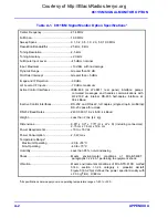
Страница 248: ...4 kBaud Inactive Control Interfaces RS 232 and RS 422 full duplex single drop multidrop RS 232 pass thru mode RS 232 Baud Rates 2400 9600 19 2 k 38 4 k Baud Weight Less than 2 lbs 4 4 kg Dimensions 0...

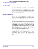
Страница 249: ...ard are set at the factory so that the WJ 8611 defaults to the IEEE 488 interface upon loss of memory Figure A 1 depicts the factory settings for the WJ 8611 s A2S1 and A2S2 configuration switches whe...

Страница 250: ...SM option 1 2 3 4 5 6 7 8 ON 98 0427 ADDRESS SINGLE DROP INTERFACE RS 422 BAUD RATE 38 4K NOTE DARK SEGMENTS DEPICT SWITCH POSITIONS Figure A 2 WJ 9168 SMM DIP Switch A2S1 As Shipped Settings for 861...

Страница 251: ...pins Pins 1 and 4 of this connector are spectrum inversion inputs associated with the SM 1 IN and the SM 2 IN RF inputs respectively These inputs can be driven by external receivers which normally hav...

Страница 252: ...2 RS 232 data 2 wire interface secondary RS232 TxD DCE O 1 2 7 O RS 232 RS 232 data 2 wire interface secondary GND 1 6 RS 232 interface ground SPTINV 1 1 I CMOS Spectrum Invert from SM 1 IN Receiver S...

Страница 253: ...nterface for use with other receivers If this alternative is desired refer to the WJ 9168 Installation Operation and Organizational Level Maintenance Manual P N 181247 001 Keep in mind that the WJ 861...

Страница 254: ...send the Built In Test command A9H See Table A 3 A 9 2 COMMAND FORMAT Each of the binary commands that control the WJ 9168 is one byte long All command bytes used in IEEE 488 applications are followe...

Страница 255: ...ee modes is arranged in relationship to the frequency spectrum being swept and is transmitted in the following format Data Point Format 1 byte data point Unipolar 8 bit binary range 0 250 data represe...

Страница 256: ...and AlH reduces the number of data points transmitted in a sweep The command allows a reduction of data points by a factor of either 2 or 4 but the sweep data is still transmitted in the standard bloc...

Страница 257: ...is sent during transmission of the data block two to four additional data points may be sent before the data stream is stopped and an ACK response to the Stop Processing command is sent CONTINUOUS SIN...

Страница 258: ...ated in Figure A 4 An upright IF spectrum would be displayed as Span Parameter 0 10 MHz Span 25 kHzStep Size 400 points sweep point 0 1 2 3 398 399 16 4 MHz 26 4MHz 397 400 16 425 MHz 16 475 MHz 16 45...

Страница 259: ...400 01H 10 MHz 25 kHz 12 5 kHz 800 02H 5 MHz 25 kHz 25 kHz 200 03H 5 MHz 25 kHz 12 5 kHz 400 04H 5 MHz 8 kHz 5 kHz 1000 05H 2 MHz 25 kHz 25 kHz 80 06H 2 MHz 25 kHz 12 5 kHz 160 07H 2 MHz 25 kHz 5 kHz...

Страница 260: ...rocessing command A3H or another command is received When the sweep parameters are changed the sweep must be restarted with the Start Processing command There is one situation that can halt the freque...

Страница 261: ...t is two byte MOD 128 7 bits each byte The most significant bit of each byte is 0 DATA FIELD Two byte tune frequency MOD 128 Parameters examples 0000H 16 4000 MHz point 0 0001H 16 4025 MHz point 1 007...

Страница 262: ...cted Active LO Default 02H Hardware Line Selected Active HI Example A701H Select Inverted Spectrum A8H Input Select Selects either IF input 1 or IF input 2 for processing DATA FIELD 01H IF Input 1 02H...

Страница 263: ...LL its 2nd LO PLL will always indicate a locked condition 4 The WJ 9168 responds with its BIT data byte immediately upon receipt and processing of the command AAH Request Unit ID Requests the WJ 9168...

Страница 264: ...cuits specifically START Fixed Tune and Signal Strength Since the micro controller is fully operational in the low power mode all setup information is retained and sweep setups may be changed Mode 1 T...

Страница 265: ...stallation and Operation Manual P N 181247 00X A 10 3 8611 SM WJ 8611 SIGNAL MONITOR OPTION Revision A 1 Signal Monitor Module 1 WJ 9168 14632 W8 Signal Monitor Control Cable 1 384477 001 14632 W9 SMA...

Страница 266: ...8611 SM SIGNAL MONITOR OPTION A 20 APPENDIX A TO A2J7 Figure A 5 8611 SM Signal Monitor Option Schematic Diagram 384476 Rev A Courtesy of http BlackRadios terryo org...

Страница 267: ...FP i FOLDOUTS Courtesy of http BlackRadios terryo org...

Страница 268: ...FP ii THIS PAGE INTENTIONALLY LEFT BLANK Courtesy of http BlackRadios terryo org...

Страница 269: ...02 5 69 7 12 46 1 82 2 95 3 48 3 89 4 37 5 88 11 000 4 250 2 70 5 24 56 1 82 2 95 4 47 1 26 1 02 1 24 95 1196 WJ 8611 IN RF TYPE SERIAL U S S U E F F E F1 IEEE 488 SDU VIDEO DIGITAL RS 232 CT EXT REF...

Страница 270: ...ENABLE REGISTER DEE DEE 00 enTHB L O G I C A L O R 07 N U 06 N U 05 N U 04 enPRS 03 N U 01 enABS 07 N U 06 N U 05 N U 04 PRS 03 N U 02 N U 01 ABS 00 THB 02 N U RECEIVER STATUS ENABLE REGISTER RSE RSE...

Страница 271: ...ES SERIAL CONTROL BUS RFB DATA CLK STB RFB A2 A1 A0 POWER INPUT 5 5 Vdc 13 5 Vdc 13 5 Vdc 24 Vdc POWER BUS 13 5 V 5 5 V 13 5 V DIGITAL IF OUTPUT CT LINE A CT LINE B SERIAL CONTROL RF16 IF16 IF8 IF4 IF...

Страница 272: ...50 MHz LP FILTER PHASE DETECTOR DIVIDE BY 8 DIVIDE BY A N COUNTER LOOP FILTER SIX BAND VCO 1370 2350 MHz DIVIDE BY 16 17 MODULUS COUNTER DIVIDE BY 2 PRESCALER 16 dB ATTENUATOR 10 MHz REFERENCE 1ST LO...

Страница 273: ...80 220 MHz 80 kHz INCREMENTS 2 25 2 749 MHz 1 kHz INCREMENTS 2ND LO VCO 1327 75 1330 25 MHz 1 kHz INCREMENTS 10 MHz TCXO 2X MULTIPLIER 10 MHz REFERENCE 3RD LO VCO CONTROL 21 65 MHz 3RDLO 20 MHZ EXTERN...

Страница 274: ...GIC CP s SERIAL INTERFACE DISTRIBUTION FPGA INTERFACE LOGIC PART OF U69 U92 U97 DSPA U2 U3 U5 U10 U100 DSPB U5 U6 U12 U13 U17 U20 U100 U108 U109 FPGA INTERFACE LOGIC PART OF U69 FPGA INTERFACE LOGIC P...

Страница 275: ...RAM 32K X 8 DATA BUS 00 15 DIGIT COLUMN DRIVER LATCH SEGMENT DRIVER LATCH DISPLAY TIMING DOT MATRIX DISPLAY DIG COL 0 7 COLUMN ENABLE DIGIT DRIVERS SEGMENT DRIVERS SEGDP 00 15 SDCLK SDATA SWITCH INDI...

Страница 276: ...UENCY MHz 1 4 2 5 7 8 3 6 9 SQL dBm BFO ZERO SQL 125 100 SIGNAL dBm GAITHERSBURG MARYLAND USA BLANKER AFC HI LO TUNE WJ 8611 VHF UHF RECEIVER IN RF Gaithersburg Maryland USA TYPE SERIAL U S S U E F F...

Страница 277: ...WJ 8611 DIGITAL VHF UHF RECEIVER FO 9 Part 482554 Front Panel Control PC Assembly A1A1 Component Location Drawing 482547 FP 17 FP 18 blank 95 1198 Courtesy of http BlackRadios terryo org...

Страница 278: ...WJ 8611 DIGITAL VHF UHF RECEIVER FO 10 Part 482929 Display PC Assembly A1A2 Component Location Drawing 482929 FP 19 FP 20 blank Courtesy of http BlackRadios terryo org...

Страница 279: ...WJ 8611 DIGITAL VHF UHF RECEIVER FO 11 Type 797168 Digital Control PC Assembly A2 Component Location Drawing 797168 Sheet 1 of 2 FP 21 FP 22 blank TOP VIEW Courtesy of http BlackRadios terryo org...

Страница 280: ...WJ 8611 DIGITAL VHF UHF RECEIVER BOTTOM VIEW FO 11 Type 797168 Digital Control PC Assembly A2 Component Location Drawing 797168 Sheet 2 of 2 FP 23 FP 24 blank Courtesy of http BlackRadios terryo org...

Страница 281: ...Part 482902 1st LO 1st Converter PC Assembly A3A1 Component Location Drawing 482902 Sheet 1 of 2 FP 25 FP 26 blank WJ 8711 DIGITAL VHF UHF RECEIVER TOP VIEW 95 1201 Courtesy of http BlackRadios terry...

Страница 282: ...DIGITAL VHF UHF RECEIVER BOTTOM VIEW 95 1201A FO 12 Part 482902 1st LO 1st Converter PC Assembly A3A1 Component Location Drawing 482902 Sheet 2 of 2 FP 27 FP 28 blank Courtesy of http BlackRadios ter...

Страница 283: ...11 DIGITAL VHF UHF RECEIVER FO 13 Part 482903 2nd LO 2nd Converter PC Assembly A3A2 Component Location Drawing 482903 Sheet 1 of 2 FP 29 FP 30 blank TOP VIEW 95 1202 Courtesy of http BlackRadios terry...

Страница 284: ...DIGITAL VHF UHF RECEIVER BOTTOM VIEW 95 1202 FO 13 Part 482903 2nd LO 2nd Converter PC Assembly A3A2 Component Location Drawing 482903 Sheet 2 of 2 FP 31 FP 32 blank Courtesy of http BlackRadios terr...

Страница 285: ...FO 14 Type 797229 2 Front Panel Assembly A1 Schematic Diagram 482930 A FP 33 FP 34 blank WJ 8611 DIGITAL VHF UHF RECEIVER Courtesy of http BlackRadios terryo org...

Страница 286: ...FO 15 Part 482554 2 Front Panel Control PC Assembly A1A1 Schematic Diagram 581643 G FP 35 FP 36 blank WJ 8611 DIGITAL VHF UHF RECEIVER Courtesy of http BlackRadios terryo org...

Страница 287: ...FO 16 Part 482929 1 Display PC Assembly A1A2 Schematic Diagram 581885 B1 FP 37 FP 38 blank WJ 8611 DIGITAL VHF UHF RECEIVER Courtesy of http BlackRadios terryo org...

Страница 288: ...WJ 8611 DIGITAL VHF UHF RECEIVER FO 17 Type 797168 1 Digital Control PC Assembly A2 Schematic Diagram 581765 Sheet 1 of 7 S FP 39 FP 40 blank Courtesy of http BlackRadios terryo org...

Страница 289: ...WJ 8611 DIGITAL VHF UHF RECEIVER FO 17 Type 797168 1 Digital Control PC Assembly A2 Schematic Diagram 581765 Sheet 2 of 7 S FP 41 FP 42 blank Courtesy of http BlackRadios terryo org...

Страница 290: ...WJ 8611 DIGITAL VHF UHF RECEIVER FO 17 Type 797168 1 Digital Control PC Assembly A2 Schematic Diagram 581765 Sheet 3 of 7 S FP 43 FP 44 blank Courtesy of http BlackRadios terryo org...

Страница 291: ...WJ 8611 DIGITAL VHF UHF RECEIVER FO 17 Type 797168 1 Digital Control PC Assembly A2 Schematic Diagram 581765 Sheet 4 of 7 S FP 45 FP 46 blank Courtesy of http BlackRadios terryo org...

Страница 292: ...WJ 8611 DIGITAL VHF UHF RECEIVER FO 17 Type 797168 1 Digital Control PC Assembly A2 Schematic Diagram 581765 Sheet 5 of 7 S FP 47 FP 48 blank Courtesy of http BlackRadios terryo org...

Страница 293: ...FO 19 Part 482902 1 1st LO 1st Converter PC Assembly A3A1 Schematic Diagram 581883 Sheet 2 of 2 R FP 57 FP 58 blank WJ 8611 DIGITAL VHF UHF RECEIVER Courtesy of http BlackRadios terryo org...

Страница 294: ...WJ 8611 DIGITAL VHF UHF RECEIVER FO 17 Type 797168 1 Digital Control PC Assembly A2 Schematic Diagram 581765 Sheet 6 of 7 S FP 49 FP 50 blank Courtesy of http BlackRadios terryo org...

Страница 295: ...WJ 8611 DIGITAL VHF UHF RECEIVER FO 17 Type 797168 1 Digital Control PC Assembly A2 Schematic Diagram 581765 Sheet 7 of 7 S FP 51 FP 52 blank Courtesy of http BlackRadios terryo org...

Страница 296: ...FO 18 Type 797228 1 RF Tuner Assembly A3 Schematic Diagram 482883 A FP 53 FP 54 blank WJ 8611 DIGITAL VHF UHF RECEIVER Courtesy of http BlackRadios terryo org...

Страница 297: ...FO 19 Part 482902 1 1st LO 1st Converter PC Assembly A3A1 Schematic Diagram 581883 Sheet 1 of 2 R FP 55 FP 56 blank WJ 8611 DIGITAL VHF UHF RECEIVER Courtesy of http BlackRadios terryo org...

Страница 298: ...Courtesy of http BlackRadios terryo org...

Страница 299: ...2 n d C o n v e r t e r P C A s s e m b l y A 3 A 2 S c h e m a t i c D i a g r a m 5 8 1 8 8 4 S h e e t 3 o f 3 A B F P 6 3 F P 6 4 b l a n k W J 8 6 1 1 D I G I T A L V H F U H F R E C E I V E R C...

Страница 300: ...Courtesy of http BlackRadios terryo org...

Страница 301: ...Courtesy of http BlackRadios terryo org...

Отзывы: